EP0516408A2 - Verfahren zur Herstellung einer T-Gatestruktur über einem Substrat mit einem mikroelektronischen Bauelement - Google Patents
Verfahren zur Herstellung einer T-Gatestruktur über einem Substrat mit einem mikroelektronischen Bauelement Download PDFInfo
- Publication number
- EP0516408A2 EP0516408A2 EP92304827A EP92304827A EP0516408A2 EP 0516408 A2 EP0516408 A2 EP 0516408A2 EP 92304827 A EP92304827 A EP 92304827A EP 92304827 A EP92304827 A EP 92304827A EP 0516408 A2 EP0516408 A2 EP 0516408A2
- Authority
- EP
- European Patent Office
- Prior art keywords
- material layer
- opening
- resist
- layer
- width
- Prior art date
- Legal status (The legal status is an assumption and is not a legal conclusion. Google has not performed a legal analysis and makes no representation as to the accuracy of the status listed.)
- Withdrawn
Links
Images


Classifications
-
- H—ELECTRICITY
- H10—SEMICONDUCTOR DEVICES; ELECTRIC SOLID-STATE DEVICES NOT OTHERWISE PROVIDED FOR
- H10D—INORGANIC ELECTRIC SEMICONDUCTOR DEVICES
- H10D30/00—Field-effect transistors [FET]
- H10D30/01—Manufacture or treatment
- H10D30/015—Manufacture or treatment of FETs having heterojunction interface channels or heterojunction gate electrodes, e.g. HEMT
-
- H—ELECTRICITY
- H10—SEMICONDUCTOR DEVICES; ELECTRIC SOLID-STATE DEVICES NOT OTHERWISE PROVIDED FOR
- H10D—INORGANIC ELECTRIC SEMICONDUCTOR DEVICES
- H10D64/00—Electrodes of devices having potential barriers
- H10D64/01—Manufacture or treatment
- H10D64/012—Manufacture or treatment of electrodes comprising a Schottky barrier to a semiconductor
- H10D64/0124—Manufacture or treatment of electrodes comprising a Schottky barrier to a semiconductor to Group III-V semiconductors
- H10D64/0125—Manufacture or treatment of electrodes comprising a Schottky barrier to a semiconductor to Group III-V semiconductors characterised by the sectional shape, e.g. T or inverted T
-
- H—ELECTRICITY
- H10—SEMICONDUCTOR DEVICES; ELECTRIC SOLID-STATE DEVICES NOT OTHERWISE PROVIDED FOR
- H10P—GENERIC PROCESSES OR APPARATUS FOR THE MANUFACTURE OR TREATMENT OF DEVICES COVERED BY CLASS H10
- H10P76/00—Manufacture or treatment of masks on semiconductor bodies, e.g. by lithography or photolithography
- H10P76/20—Manufacture or treatment of masks on semiconductor bodies, e.g. by lithography or photolithography of masks comprising organic materials
- H10P76/202—Manufacture or treatment of masks on semiconductor bodies, e.g. by lithography or photolithography of masks comprising organic materials for lift-off processes
-
- Y—GENERAL TAGGING OF NEW TECHNOLOGICAL DEVELOPMENTS; GENERAL TAGGING OF CROSS-SECTIONAL TECHNOLOGIES SPANNING OVER SEVERAL SECTIONS OF THE IPC; TECHNICAL SUBJECTS COVERED BY FORMER USPC CROSS-REFERENCE ART COLLECTIONS [XRACs] AND DIGESTS
- Y10—TECHNICAL SUBJECTS COVERED BY FORMER USPC
- Y10S—TECHNICAL SUBJECTS COVERED BY FORMER USPC CROSS-REFERENCE ART COLLECTIONS [XRACs] AND DIGESTS
- Y10S438/00—Semiconductor device manufacturing: process
- Y10S438/909—Controlled atmosphere
-
- Y—GENERAL TAGGING OF NEW TECHNOLOGICAL DEVELOPMENTS; GENERAL TAGGING OF CROSS-SECTIONAL TECHNOLOGIES SPANNING OVER SEVERAL SECTIONS OF THE IPC; TECHNICAL SUBJECTS COVERED BY FORMER USPC CROSS-REFERENCE ART COLLECTIONS [XRACs] AND DIGESTS
- Y10—TECHNICAL SUBJECTS COVERED BY FORMER USPC
- Y10S—TECHNICAL SUBJECTS COVERED BY FORMER USPC CROSS-REFERENCE ART COLLECTIONS [XRACs] AND DIGESTS
- Y10S438/00—Semiconductor device manufacturing: process
- Y10S438/942—Masking
- Y10S438/948—Radiation resist
- Y10S438/949—Energy beam treating radiation resist on semiconductor
-
- Y—GENERAL TAGGING OF NEW TECHNOLOGICAL DEVELOPMENTS; GENERAL TAGGING OF CROSS-SECTIONAL TECHNOLOGIES SPANNING OVER SEVERAL SECTIONS OF THE IPC; TECHNICAL SUBJECTS COVERED BY FORMER USPC CROSS-REFERENCE ART COLLECTIONS [XRACs] AND DIGESTS
- Y10—TECHNICAL SUBJECTS COVERED BY FORMER USPC
- Y10S—TECHNICAL SUBJECTS COVERED BY FORMER USPC CROSS-REFERENCE ART COLLECTIONS [XRACs] AND DIGESTS
- Y10S438/00—Semiconductor device manufacturing: process
- Y10S438/942—Masking
- Y10S438/948—Radiation resist
- Y10S438/951—Lift-off
Definitions
- the present invention relates to a method of forming a T-gate structure for a microelectronic device such as a high-electron mobility transistor (HEMT) on the surface of a substrate.
- a microelectronic device such as a high-electron mobility transistor (HEMT)
- the HEMT is a variant of gallium arsenide field effect transistor (FET) technology that offers substantially better performance than standard metal-semiconductor field effect transistor (MESFET) devices, particularly at low temperatures.
- HEMT substrates are usually fabricated by molecular beam epitaxy (MBE), in which the device layers are built up by deposition of molecules in a vacuum.
- MBE molecular beam epitaxy
- a conventional HEMT uses an undoped gallium arsenide (GaAs) channel which is supplied with electrons by a thin aluminum gallium arsenide (AlGaAs) doping layer between the channel and the controlling gate electrode. This separation of the channel dopant layer, where electron scattering is high, from the channel itself, significantly increases the mobility of the electrons in the channel. It is the high mobility of the carriers that provides the fundamental advantage of HEMT technology over conventional MESFET devices in high frequency operation.
- HEMT devices In order to achieve the highest frequency operation from HEMT devices, it is also necessary to reduce the distances over which the gate's field effect control of the electrons in the channel must take place, thereby reducing the parasitic resistances and capacitances that limit device speed.
- the primary critical dimension concerned is the length of the gate electrode itself, which defines the distance the electrons must traverse underneath the gate during the operation of the device. A shorter gate length decreases the transit time for carriers in the channel, however, it also increases the series resistance of the gate electrode itself, slowing down the device. Therefore, it is desirable for a HEMT device to have a T-shaped gate, in order to provide a short gate length to the channel in combination with a wide upper cross section for low gate series resistance.
- the conventional method of forming a T-gate structure relies on either a two layer or three layer resist technology in combination with electron beam exposure.
- the upper layer is more sensitive to the electron beam exposure, while the lower layer is less sensitive.
- the upper more sensitive layer develops into a wide cavity, while the lower layer develops to a narrower width, creating a "wine goblet" shaped cavity.
- Metal is deposited onto the substrate which fills the cavity and forms the desired T-shaped gate therein.
- the resist layers and overlying metal are removed by dissolving the resist layers and lifting off the metal, leaving the T-gate structure on the surface of the substrate.
- the bilevel and trilevel resist methods with electron beam exposure have been used to fabricate T-gate structures with gate lengths as short as approximately 50 nm. This has enabled the fabrication of HEMTs with current-gain cutoff frequency f T of up to 250 GHz.
- both of these methods are inherently limited in resolution since the gate length is defined at the bottom of the resist structure, after the electron beam has passed through the entire thickness of the resist layers. Since the extremely light electrons are scattered as the beam passes through the resist, the resolution of the exposure degrades by the time the beam reaches the bottom of the resist.
- higher resolution can be obtained in thin resist imaging layers, there have not been any practical methods proposed to date of providing a thin imaging layer technique for fabricating T-Gate structures.
- the present method provides a method for forming a T-shaped gate for a HEMT or other microelectronic device on a surface of a substrate.
- the method utilizes a thin surface imaging layer, maximizing the obtainable resolution in the exposure, and then transfers the exposure down to the subsequent resist layers without loss of resolution using a novel two step reactive ion etching technique.
- This method enables the fabrication of T-gate structures limited only by the beam width of the exposure system (typically 5 - 10 nm) and the edge acuity of anisotropic reactive ion etching (RIE), which is typically 5 - 10 nm.
- RIE anisotropic reactive ion etching
- the substrate will typically consist of a contact layer, Schottky barrier layer, donor layer, spacer layer, channel and buffer layers which are epitaxially deposited on a substrate wafer such as gallium arsenide.
- a first resist layer is formed on the surface of the substrate.
- the first resist layer is a planarizing layer of poly-methyl-methacrylate (PMMA).
- a masking layer of germanium (Ge) is formed over the resist layer, and a second imaging layer of PMMA is formed over the masking layer, forming a three layer or trilevel resist structure.
- the PMMA imaging layer is exposed to a focused ion beam (FIB) having a beam width substantially equal to the desired gate length of the T-gate structure, and developed therethrough having a width equal to the gate length.
- FIB focused ion beam
- the masking layer of germanium is anisotropically etched by RIE through the opening in the second resist layer to extend the opening through the masking layer with the same gate length dimension.
- the first, or planarizing resist layer is then etched down to the substrate with a novel, two step RIE technique.
- the planarizing resist layer is isotropically etched through the opening in the masking layer partially through to the substrate surface using RIE to form a cavity in the first resist layer, underneath the opening, having a width which is larger than that of the opening.
- the remaining thickness of the first resist layer is then etched through the opening, completely through to the substrate surface with an anisotropic RIE process, that forms a high resolution notch, extending from the bottom of the cavity in the first resist layer to the substrate surface, of a width substantially equal to the same gate length as the mask layer opening.
- the second, imaging resist layer is generally removed during these same isotropic and anisotropic RIE steps.
- the masking layer is then removed, using an anisotropic RIE process, leaving a "wine goblet" shaped resist profile in the remaining planarizing resist layer.
- the uppermost layer of the MBE grown substrate, the ohmic contact layer is typically removed at this point.
- An electrically conductive metal is then deposited over the first resist layer into the cavity and notch, such that the conductive metal adheres to the substrate surface at the bottom of the notch.
- the conductive material in the cavity and notch form the T-gate structure.
- the first resist layer and overlying metal are lifted off to leave the T-gate structure on the substrate.
- the source, drain and other elements of the microelectronic device are then fabricated on the substrate surface.
- the scope of the invention is not so limited, and further includes imaging using a an electron beam, optical beam or x-ray beam.
- the preferred embodiment of etching the planarizing layer is using RIE, the scope of the invention is not so limited, and further includes other etching techniques such as plasma etching, magnetron enhanced reactive ion etching, radical ion beam etching and electron cyclotron resonance etching techniques.
- the order of the isotropic and anisotropic RIE steps may be reversed, thereby forming a high resolution notch partially or entirely through the planarizing resist layer, and then forming a wider cavity in the upper section of the planarizing layer using isotropic RIE.
- the imaging resist layer and the masking layer may be replaced by a single resist layer which has the function of these two layers combined, such as a single resist layer formed of a self-developing organosilicon film.
- the present method enables the fabrication of T-gate structures in thick resist layers with gate lengths limited only by the exposing beam width of the exposure technique and the edge acuity of RIE. Loss of resolution of the exposure image is negligible due to the ability to make the imaging resist layer extremely thin. Additionally, the extremely high edge acuity available with RIE is able to transfer that image down through thick imaging layers with minimal loss of resolution. Thus the present method enables precise pattern definition at the bottom of the resist, which defines the critical gate length of the T-gate structure, in a manner not possible using the prior art electron beam process.
- the present invention is completely compatible with the highly perferable self-aligned gate HEMT fabrication techniques, which further improves the frequency response of the HEMT devices.
- the method of the present invention includes providing a substrate 10 as illustrated in FIG. 1.
- the substrate 10 includes a wafer made of a semiconductive or semi-insulating material, preferably GaAs or InP, onto which the necessary buffer, superlattice, channel, spacer, donor, Schottky barrier and contact layers are formed epitaxially on the wafer to constitute a layered structure for a HEMT or other microelectronic device.
- the surface of the upper epitaxial layer of the substrate 10 is considered to be the surface 10a of the substrate 10. It will be noted that in a recessed gate configuration (not shown), the exposed walls of the recess are considered to be part of the surface 10a.
- a planarizing or first resist layer 12 is deposited over the surface 10a of the substrate 10.
- the layer 12 is preferably formed of PMMA to a thickness of approximately 500 nm.
- a masking layer 14 of low stress germanium (Ge) or silicon (Si) is deposited over the first resist layer 12 to a thickness of approximately 15 nm.
- a second imaging resist layer of PMMA is then deposited over the masking layer 12 to a thickness of approximately 60 nm.
- planarizing polymer resist materials such as standard optical photoresists, electron beam resists or plasma deposited polymers can function in place of the PMMA planarizing layer.
- a variety of thin metal layers may also be substituted for the germanium and silicon layers, such as tungsten, titanium, tantalum or aluminum, within the scope of the present invention.
- Other thin imaging layers can also be substituted for the thin PMMA layer, as may be appropriate if an exposure technique other than FIB is used, and are also within the scope of the invention.
- the second resist layer 16 is exposed to an imaging exposure using a beam as designated by arrows 18, the exposed region having a width W which is substantially equal to the desired gate length of the T-gate structure.
- the beam 18 is a focused ion beam (FIB) of 50 keV gallium (Ga) ions with a beam width of approximately 10 nm.
- FIB focused ion beam
- the scope of the invention further includes imaging the layer 16 using an electron beam, optical beam, or x-ray beam.
- the exposed second resist layer 16 is then developed using a conventional resist developer, such as a solution of three parts isopropyl alcohol, one part methylisobutyl-ketone, for 15 seconds followed by a 60 second isopropyl alcohol rinse, to form an opening 16a through the layer 16 having substantially the width W.
- a conventional resist developer such as a solution of three parts isopropyl alcohol, one part methylisobutyl-ketone, for 15 seconds followed by a 60 second isopropyl alcohol rinse, to form an opening 16a through the layer 16 having substantially the width W.
- the masking layer 14 is etched through the opening 16a in the layer 16 as indicated by arrows 20 to extend the opening 16a down to the first resist layer 12.
- the opening through the masking layer 14 is designated as 14a.
- the step of FIG. 3 is preferably performed using RIE with carbon tetrafluoride (CF4) plasma at a flow rate of 20 cm3/min, chamber pressure of 50 mTorr, plasma potential of 45 volts, and etch rate of 7.8 nm/min, although the invention is not so limited.
- CF4 carbon tetrafluoride
- the etchant used in the step of FIG. 3 is selected such that it will not significantly affect the layers 16 and 12 while etching through the masking layer 14.
- the second resist layer 16 therefore acts as a mask during the etching step, such that the masking layer 14 will only be etched through the opening 16a. Due to the very thin masking layer (15 nm), the width of the opening 14a is substantially equal to the width W of the opening 16a.
- the masking layer 14 can be made thicker and still be used in accordance with the invention as long as the etching process 20 used to create the opening is sufficiently anisotropic to create an opening 14a that is substantially equal to the desired width W.
- the first resist layer 12 is etched through the openings 14a and 16a using isotropic RIE as indicated by arrows 22 to form a cavity 12a therein.
- the isotropic etching undercuts the masking layer 14 so that the cavity 12a is considerably wider than the width W of the openings 14a and 16a.
- the cavity 12a will preferably be etched to a width on the order of 100 - 250 nm.
- the isotropic RIE step of FIG. 4 is preferably performed using an oxygen (O2) plasma at a flow rate of 20 cm3/min, a chamber pressure of 90 mTorr and a plasma potential -75 volts.
- O2 oxygen
- the preferred etch rate is 17.5 nm/min. It will be understood, however, that these values do not limit the scope of the invention. It is also possible to practice the invention as described, using methods other than reactive ion etching (RIE) for the isotropic etching process 22.
- etching methods including standard plasma etching, magnetically enhanced reactive ion etching, electron cyclotron resonance, reactive ion beam ion etching, microwave plasma etching or radical beam etching, can also be used for the isotropic etching process 22, within the scope of the present invention, as long as the etching process used produces the desired isotropic etching result.
- the isotropic RIE with oxygen plasma also removes the second resist layer 16 from the masking layer 14.
- the etchant used in the step of FIG. 4 is selected such that it will not significantly affect the masking layer 14.
- the next step of the method is illustrated in FIG. 5.
- the first resist layer 12 is etched through the opening 14a in the masking layer 14 using anisotropic RIE as indicated by arrows 24 to form a notch 12b underneath the cavity 12a.
- the notch 12b extends completely down to the surface 10a of the substrate 10. Due to the anisotropic nature of the etching, the width of the notch 12b is substantially equal to W.
- the anisotropic RIE step of FIG. 5 is preferably performed using an O2 plasma at a flow rate of 20 cm3/min, chamber pressure of 2 mTorr and a plasma potential of -45 volts.
- the preferred etch rate is 7 nm/min.
- the extremely low pressure reduces the scattering of the ions in the RIE plasma and produces an etching profile that is highly anisotropic.
- This highly anisotropic property combined with the fact that the O2 plasma does not appreciably alter the masking layer 14, causes the notch 12b to only be etched in the area of the first resist layer 12 directly underlying the opening 14a.
- the step of FIG. 5 is performed at low plasma potential to avoid damaging the substrate 10 when the notch 12b has been etched completely through the first resist layer 12 to the surface 10a.
- anisotropic etching process 24 it is also possible to practice this invention using an alternative method for the anisotropic etching process 24.
- alternative etching methods using standard plasma etching, magnetically enhanced reactive ion etching, electron cyclotron resonance, reactive ion beam ion etching, microwave plasma etching or radical beam etching, can also be used for the anisotropic etching process 24, within the scope of the present invention, as long as the etching process used produces the desired anisotropic etching result.
- the steps of the method described above form the opening 16b in the relatively thin second resist layer 16 having the width W desired for the gate length of the T-gate structure, and precisely extend the opening 16a down through the masking layer 14 and second resist layer 16 to form the notch 12b with substantially the same width as the opening 16a.
- the notch 12b defines the bottom of the desired T-gate structure, while the wider cavity 12a defines the top of the structure.
- the masking layer 14 is removed using a wet chemical solution or RIE etching with CF4 plasma as indicated by arrows 26 to leave only the first resist layer 12 remaining on the substrate 10 with the cavity 12a and notch 12b formed therein.
- the preferred embodiment uses a RIE etching process with a 20 cm3/min CF4 flow rate, 50 mTorr chamber pressure, -45 Volts plasma potential and an etch rate of 7.8 nm/min, although the invention is not so limited.
- the remaining resist cavity 12a is such that it contains an overhang of too great an extent, it can be removed with a short, low pressure and low plasma potential anisotropic O2 RIE process step before proceeding to the process step illustrated in FIG. 7. In the preferred embodiment, this step is omitted because the overhang produced by the isotropic etching of the resist cavity 12a is already suitable for the subsequent processing steps.
- the contact layer is usually removed in the gate region at this point, forming a recessed surface, using the resist layer 12 as a mask.
- the walls of the recess are considered to be a part of the surface 10a.
- an electrically conductive metal 28 preferably in the form of a multi-layer metal structure including layers of titanium (Ti), platinum (Pt), and gold (Au), is evaporated onto the first resist layer 12 and into the cavity 12a and notch 12b as indicated by arrows 30 such that the metal 28 adheres to the surface 10a of the substrate 10 at the bottom of the notch 12b, forming a Schottky barrier contact.
- the portion of the metal 28 in the cavity 12a and notch 12b constitutes the desired T-gate structure, which is designated as 28a.
- the first resist layer 12 and overlying metal 28 are lifted off by dissolving the layer 12 in a conventional solvent, such a methylene-chloride, to leave only the T-gate structure 28a remaining on the surface 10a of the substrate 10.
- a conventional solvent such as a methylene-chloride
- a microelectronic device such.as a HEMT or other FET incorporating the T-gate structure 28a may be fabricated using additional process steps such as illustrated in FIG. 9.
- an electrically conductive metal 32 preferably in the form of a multi-layer metal structure including layers of alloyed gold and germanium, nickel (Ni), and gold, is deposited onto the substrate 10 as indicated by arrows 34.
- the top of the T-gate structure 28a acts as a mask such that no metal 32 is deposited onto the surface 10a underneath the structure 28.
- a portion of the metal 32 is deposited onto the top of the structure 28a as designated at 32a, which is desirable since it increases the cross sectional area of the structure 28a, reducing the series resistance of the gate electrode.
- Another portion of the metal 32 is deposited onto the surface 10a leftward of the structure 28a to form a source 36 of an FET 38. Another portion of the metal 32 deposited rightward of the structure 28a to form a drain 40 of the FET 38.
- the spacing between the source 36 and drain 38 define the channel length of the FET 38, which is substantially equal to the width of the top of the T-gate structure 28a.
- the source/drain contacts and channel of the FET 38 are self-aligned to the gate in the process step of FIG. 9.
- the source/drain contacts are not self-aligned to the gate, as described here.
- the gate itself is fabricated as outlined by the methods herein, it is considered to be within the scope of this invention.
- FIGs. 10 to 13 Another alternative method of practicing the present invention is illustrated in FIGs. 10 to 13, in which the isotropic and anisotropic RIE steps are reversed.
- the first resist layer 12, masking layer 14 and second resist layer 16 are deposited on the substrate 10 and formed with the openings 14a and 16a in the same manner as in FIGs. 1 to 3.
- a notch 12c is formed completely through the first resist layer 12 using low pressure, low voltage anisotropic RIE as indicated by arrows 42.
- the width of the notch 12c is substantially equal to W.
- the etching step of FIG. 10 also removes the second resist layer 16 from the masking layer 14.
- high pressure isotropic RIE is performed using O2 plasma as indicated by arrows 44 to form a cavity 12d underlying the opening 14a having a width which is considerably larger than W.
- the isotropic RIE step is also performed at low plasma potential, typically less than -45 Volts, in order to prevent damage to the underlying HEMT device.
- the masking layer 14 is removed in the step illustrated in FIG. 12 using RIE with a CF4 plasma as indicated by arrows 46. The conditions for the removal of the masking layer 14 will generally be similar to those described above, with reference to FIG. 6.
- low voltage anisotropic RIE is performed using an O2 plasma as indicated by arrows 48.
- This step causes the overhang of the resist cavity 12a to be removed and as described previously, may not be necessary if the overhang is already suitable.
- the conditions under which the isotropic and anisotropic RIE steps are performed will generally be similar to those described above with reference to FIGs. 1 to 6.
- the steps of FIGs. 7 to 9 may then be performed to form a T-gate structure and associated elements in the same manner as with the structure illustrated in FIG. 6.
- FIGs. 14 to 18 Another method of practicing the present invention is illustrated in FIGs. 14 to 18, in which the masking layer 14 and second resist layer 16 are incorporated into a single resist layer 50.
- the resist layer 50 is formed over the first resist layer 12, and consists of a material which is sensitive to FIB, electron beam, optical beam or x-ray beam imaging as appropriate to provide the function of the second resist layer 16, and also contains a material such as silicon, which resists the oxygen etching step, to provide the function of the masking layer 14.
- the resist layer 50 is imaged with an FIB, electron beam, optical beam or X-ray beam as indicated by arrows 52, and developed to form an opening 50a which is equivalent to the openings 14a and 16a in combination.
- the resist layer 50 may alternatively be formed of a self-developing organosilicon film such as described in an article entitled "Plasma-deposited organosilicon thin films as dry resists for deep ultraviolet lithography", by M. Horn et al, in the Journal of Vacuum Science Technology, B, Vol. 8, No. 6, Nov./Dec. 1990, pp. 1493-1496, in which case a separate developing step is not required. Then, as illustrated in FIG.
- isotropic RIE is performed using O2 plasma to form the cavity 12a in the first resist layer 12 under the opening 50a.
- the silicon in the resist layer 50 is oxidized by the plasma, and forms a silicon dioxide coating on the exposed surface of the layer 50 which resists further etching by the O2 plasma.
- anisotropic RIE is performed using an O2 plasma as indicated by arrows 56 to transfer the opening 50a down through the bottom of the cavity 12a to form the notch 12b in the manner described above in reference to FIG. 5.
- Etching with CF4 is then performed as indicated by arrows 58 in FIG. 18 to remove the resist layer 50 and leave only the first resist layer 12 having the cavity 12a and notch 12b therein remaining on the substrate 10.
- the conditions under which the isotropic and anisotropic RIE steps are performed will generally be similar to those described above with reference to FIGs. 1 to 6. Should an unsuitable overhang remain after the isotropic RIE step, a removal step may also be inserted as described previously.
- the steps of FIGs. 7 to 9 may then be performed to form a T-gate structure and associated elements in the same manner as with the structure illustrated in FIG. 6.
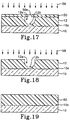
- FIGs. 19 to 25 Yet another method of practicing the present invention using a single resist layer is illustrated in FIGs. 19 to 25.
- This method utilizes a Positive Resist IMage by Etching (PRIME) process which is described in an article entitled "Positive resist image by dry etching: New dry developed positive working system for electron beam and deep ultraviolet lithography", by C. Pierrat et al, in the Journal of Vacuum Science Technology B, Vol. 7, No. 6, Nov./Dec. 1989, pp. 1782-1786.
- PRIME Positive Resist IMage by Etching
- FIG. 19 illustrates the substrate 10 with a primary resist layer 60 formed on the surface 10a thereof.
- the layer 60 is preferably formed of PLASMASK resist manufactured by U.C.B. Electronics, HPR 206 resist manufactured by Olin Hunt, PR 1024 manufactured by MacDermid, or other positive novolac based resist.
- the layer 60 is applied to the substrate 10 by coating and soft baking.
- the resist layer 60 is exposed to an electron beam, focused ion beam, optical beam in the deep ultraviolet wavelength region, or x-ray beam having a width substantially equal to the desired gate length of the T-gate structure as indicated by arrows 62.
- the power level of the image beam 62 is selected such that the beam 62 penetrates partially through the layer 60 in an area 60a to cause crosslinking between novolac chains in the material thereof.
- the resist layer 60 is irradiated with a flood optical beam as indicated by arrows 64 in the near ultraviolet wavelength region. This promotes diffusion and reaction of HMDS in the areas of the layer 60 other than the area 60a.
- the resist layer 60 is subjected to a pre-silylation bake step, followed by a silylation step as indicated by arrows 66.
- the steps may be performed at the same or different temperatures, typically on the order of 160 °C, in an oven which is evacuated for the pre-silylation bake step.
- Hexamethyldisilazane (HMDS) saturated nitrogen is caused to flow through the oven for the silylation step.
- Silylation occurs in an upper portion 60b of the resist layer 60 except for the area 60a during the silylation step illustrated in FIG. 22 due to enhancement of diffusion and reaction of HMDS induced by the near ultraviolet exposure in the step of FIG. 21.
- crosslinking inhibits HMDS diffusion in the area 60a.
- isotropic RIE using O2 plasma is performed as indicated by arrows 68 which etches away the area 60a of the layer 60 and forms an opening 60c in the upper portion of the area 60a.
- the RIE further extends through the opening 60c to form a cavity 60d in the layer 60 which is underneath and wider than the opening 60c.
- silicon (diffused from the HMDS) in the material of the layer 60 chemically transforms the upper portion 60b of the layer 60 into silicon dioxide which constitutes an in-situ mask corresponding to the masking layer 14 illustrated in FIGs. 1 to 5.
- the silicon dioxide is resistant to etching by the O2 plasma.
- anisotropic RIE using O2 plasma is performed as indicated by arrows 70 to transfer an image of the opening 60c down through the bottom of the cavity 60d to the surface 10a of the substrate 10 to form a notch 60e having substantially the same width as the opening 60c.
- RIE using CF4 plasma is performed as indicated by arrows 72 to etch away the silicon dioxide upper portion 60b of the layer 60.
- a substantial overhang remains on the cavity 60d, it may be removed with a low pressure, low voltage oxygen anisotropic RIE step as described previously.
- the result of these steps is to leave the resist layer 60 with the cavity 60d and notch 60e formed therein.
- the conditions under which the isotropic and anisotropic RIE steps are performed will generally be similar to those described above with reference to FIGs. 1 to 6. It is also understood that other plasma etching techniques such as may substituted for the isotropic and anisotropic RIE steps, as described previously.
- the steps of FIGs. 7 to 9 may then be performed to form a T-gate structure and associated elements in the same manner as with the structure illustrated in FIG. 6.
- T-gate structures were fabricated on GaAs substrates with 50 - 60 nm gate lengths, a source/drain spacing (determined by the width of the cavity formed in the isotropic RIE step) of 225 nm and a gate cross section of 0.15 um2.
Landscapes
- Junction Field-Effect Transistors (AREA)
- Electrodes Of Semiconductors (AREA)
Applications Claiming Priority (2)
| Application Number | Priority Date | Filing Date | Title |
|---|---|---|---|
| US07/705,870 US5155053A (en) | 1991-05-28 | 1991-05-28 | Method of forming t-gate structure on microelectronic device substrate |
| US705870 | 1996-08-28 |
Publications (2)
| Publication Number | Publication Date |
|---|---|
| EP0516408A2 true EP0516408A2 (de) | 1992-12-02 |
| EP0516408A3 EP0516408A3 (en) | 1993-01-13 |
Family
ID=24835293
Family Applications (1)
| Application Number | Title | Priority Date | Filing Date |
|---|---|---|---|
| EP19920304827 Withdrawn EP0516408A3 (en) | 1991-05-28 | 1992-05-28 | Method of forming t-gate structure on microelectronic device substrate |
Country Status (4)
| Country | Link |
|---|---|
| US (1) | US5155053A (de) |
| EP (1) | EP0516408A3 (de) |
| JP (1) | JPH0689907A (de) |
| IL (1) | IL102041A (de) |
Cited By (1)
| Publication number | Priority date | Publication date | Assignee | Title |
|---|---|---|---|---|
| EP0978873A1 (de) * | 1998-08-06 | 2000-02-09 | Siemens Aktiengesellschaft | Halbleiterstrukturen und Herstellungsverfahren |
Families Citing this family (45)
| Publication number | Priority date | Publication date | Assignee | Title |
|---|---|---|---|---|
| US5334542A (en) * | 1991-11-27 | 1994-08-02 | Oki Electric Industry Co., Ltd. | Method of forming T-shaped electrode |
| JPH0653241A (ja) * | 1992-08-03 | 1994-02-25 | Nec Corp | 電界効果トランジスタの製造方法 |
| US5288660A (en) * | 1993-02-01 | 1994-02-22 | Avantek, Inc. | Method for forming self-aligned t-shaped transistor electrode |
| US5436201A (en) * | 1993-05-28 | 1995-07-25 | Hughes Aircraft Company | Dual etchant process, particularly for gate recess fabrication in GaAs MMIC chips |
| FR2711451B1 (fr) * | 1993-10-18 | 1995-11-17 | Jackie Etrillard | Procédé d'obtention de contacts conducteurs auto-alignés pour composants électroniques. |
| US5489539A (en) * | 1994-01-10 | 1996-02-06 | Hughes Aircraft Company | Method of making quantum well structure with self-aligned gate |
| US5543253A (en) * | 1994-08-08 | 1996-08-06 | Electronics & Telecommunications Research Inst. | Photomask for t-gate formation and process for fabricating the same |
| US5516710A (en) * | 1994-11-10 | 1996-05-14 | Northern Telecom Limited | Method of forming a transistor |
| US6294799B1 (en) * | 1995-11-27 | 2001-09-25 | Semiconductor Energy Laboratory Co., Ltd. | Semiconductor device and method of fabricating same |
| US5940732A (en) | 1995-11-27 | 1999-08-17 | Semiconductor Energy Laboratory Co., | Method of fabricating semiconductor device |
| TW301061B (en) * | 1996-06-07 | 1997-03-21 | Ind Tech Res Inst | Manufacturing method of submicron T-type gate |
| KR100212455B1 (ko) * | 1996-11-04 | 1999-08-02 | 정선종 | 이중 게이트 구조의 반도체 소자 제조 방법 |
| DE19717363C2 (de) * | 1997-04-24 | 2001-09-06 | Siemens Ag | Herstellverfahren für eine Platinmetall-Struktur mittels eines Lift-off-Prozesses und Verwendung des Herstellverfahrens |
| TW347561B (en) * | 1997-06-20 | 1998-12-11 | Ti Acer Co Ltd | Method of forming a T-gate Lightly-Doped Drain semiconductor device |
| KR100264773B1 (ko) * | 1998-04-02 | 2000-09-01 | 윤종용 | 자기 정렬된 콘택홀을 갖는 반도체 장치의제조 방법 |
| US6833079B1 (en) * | 2000-02-17 | 2004-12-21 | Applied Materials Inc. | Method of etching a shaped cavity |
| US6319802B1 (en) | 2000-07-20 | 2001-11-20 | Advanced Micro Devices, Inc. | T-gate formation using modified damascene processing with two masks |
| US6270929B1 (en) * | 2000-07-20 | 2001-08-07 | Advanced Micro Devices, Inc. | Damascene T-gate using a relacs flow |
| US7008832B1 (en) | 2000-07-20 | 2006-03-07 | Advanced Micro Devices, Inc. | Damascene process for a T-shaped gate electrode |
| US6255202B1 (en) | 2000-07-20 | 2001-07-03 | Advanced Micro Devices, Inc. | Damascene T-gate using a spacer flow |
| US6417084B1 (en) | 2000-07-20 | 2002-07-09 | Advanced Micro Devices, Inc. | T-gate formation using a modified conventional poly process |
| US6403456B1 (en) | 2000-08-22 | 2002-06-11 | Advanced Micro Devices, Inc. | T or T/Y gate formation using trim etch processing |
| US6313019B1 (en) | 2000-08-22 | 2001-11-06 | Advanced Micro Devices | Y-gate formation using damascene processing |
| DE10101825B4 (de) * | 2001-01-17 | 2006-12-14 | United Monolithic Semiconductors Gmbh | Verfahren zur Herstellung eines Halbleiter-Bauelements mit einer T-förmigen Kontaktelektrode |
| DE10304722A1 (de) * | 2002-05-11 | 2004-08-19 | United Monolithic Semiconductors Gmbh | Verfahren zur Herstellung eines Halbleiterbauelements |
| US20040145030A1 (en) * | 2003-01-28 | 2004-07-29 | Meagley Robert P. | Forming semiconductor structures |
| US7262070B2 (en) * | 2003-09-29 | 2007-08-28 | Intel Corporation | Method to make a weight compensating/tuning layer on a substrate |
| JP4758170B2 (ja) * | 2005-08-09 | 2011-08-24 | 三菱電機株式会社 | 半導体装置の製造方法 |
| US7892978B2 (en) | 2006-07-10 | 2011-02-22 | Micron Technology, Inc. | Electron induced chemical etching for device level diagnosis |
| US7807062B2 (en) * | 2006-07-10 | 2010-10-05 | Micron Technology, Inc. | Electron induced chemical etching and deposition for local circuit repair |
| US7791055B2 (en) | 2006-07-10 | 2010-09-07 | Micron Technology, Inc. | Electron induced chemical etching/deposition for enhanced detection of surface defects |
| US7791071B2 (en) | 2006-08-14 | 2010-09-07 | Micron Technology, Inc. | Profiling solid state samples |
| US7833427B2 (en) | 2006-08-14 | 2010-11-16 | Micron Technology, Inc. | Electron beam etching device and method |
| US7718080B2 (en) * | 2006-08-14 | 2010-05-18 | Micron Technology, Inc. | Electronic beam processing device and method using carbon nanotube emitter |
| US7569484B2 (en) * | 2006-08-14 | 2009-08-04 | Micron Technology, Inc. | Plasma and electron beam etching device and method |
| US8420978B2 (en) * | 2007-01-18 | 2013-04-16 | The Board Of Trustees Of The University Of Illinois | High throughput, low cost dual-mode patterning method for large area substrates |
| US8003300B2 (en) * | 2007-04-12 | 2011-08-23 | The Board Of Trustees Of The University Of Illinois | Methods for fabricating complex micro and nanoscale structures and electronic devices and components made by the same |
| US8652763B2 (en) * | 2007-07-16 | 2014-02-18 | The Board Of Trustees Of The University Of Illinois | Method for fabricating dual damascene profiles using sub pixel-voting lithography and devices made by same |
| US8546067B2 (en) * | 2008-03-21 | 2013-10-01 | The Board Of Trustees Of The University Of Illinois | Material assisted laser ablation |
| US8187795B2 (en) * | 2008-12-09 | 2012-05-29 | The Board Of Trustees Of The University Of Illinois | Patterning methods for stretchable structures |
| WO2012094357A2 (en) * | 2011-01-07 | 2012-07-12 | Eastman Kodak Company | Transistor including multiple reentrant profiles |
| US8847226B2 (en) | 2011-01-07 | 2014-09-30 | Eastman Kodak Company | Transistor including multiple reentrant profiles |
| CN118946242A (zh) * | 2017-08-31 | 2024-11-12 | 谷歌有限责任公司 | 使用多层堆叠制造器件的方法 |
| CN111640795A (zh) * | 2020-04-28 | 2020-09-08 | 西安电子科技大学 | 一种具有弧形栅电极的氮化镓高频晶体管及制作方法 |
| CN112885899A (zh) * | 2020-12-17 | 2021-06-01 | 南京中电芯谷高频器件产业技术研究院有限公司 | 一种自对准低欧姆接触电阻GaN HEMT器件及其制造方法 |
Family Cites Families (13)
| Publication number | Priority date | Publication date | Assignee | Title |
|---|---|---|---|---|
| JPS55163860A (en) * | 1979-06-06 | 1980-12-20 | Toshiba Corp | Manufacture of semiconductor device |
| JPS57183037A (en) * | 1981-05-06 | 1982-11-11 | Nec Corp | Formation of pattern |
| JPS60111474A (ja) * | 1983-11-22 | 1985-06-17 | Nec Corp | 半導体装置の製造方法 |
| JPS6180870A (ja) * | 1984-09-27 | 1986-04-24 | Nec Corp | 半導体トランジスタおよびその製造方法 |
| JPS62250674A (ja) * | 1986-04-23 | 1987-10-31 | Nec Corp | 半導体装置の製造方法 |
| US4700462A (en) * | 1986-10-08 | 1987-10-20 | Hughes Aircraft Company | Process for making a T-gated transistor |
| JPS63155770A (ja) * | 1986-12-19 | 1988-06-28 | Hitachi Ltd | 電界効果トランジスタの製造方法 |
| US4771017A (en) * | 1987-06-23 | 1988-09-13 | Spire Corporation | Patterning process |
| JPH0269936A (ja) * | 1988-07-28 | 1990-03-08 | Siemens Ag | 半導体材料上の樹脂構造の形成方法 |
| US4959326A (en) * | 1988-12-22 | 1990-09-25 | Siemens Aktiengesellschaft | Fabricating T-gate MESFETS employing double exposure, double develop techniques |
| DE3901288A1 (de) * | 1989-01-18 | 1990-07-26 | Licentia Gmbh | Verfahren zur herstellung von gate-elektroden |
| JP2550412B2 (ja) * | 1989-05-15 | 1996-11-06 | ローム株式会社 | 電界効果トランジスタの製造方法 |
| US5053348A (en) * | 1989-12-01 | 1991-10-01 | Hughes Aircraft Company | Fabrication of self-aligned, t-gate hemt |
-
1991
- 1991-05-28 US US07/705,870 patent/US5155053A/en not_active Expired - Lifetime
-
1992
- 1992-05-28 EP EP19920304827 patent/EP0516408A3/en not_active Withdrawn
- 1992-05-28 IL IL10204192A patent/IL102041A/en unknown
- 1992-05-28 JP JP4137107A patent/JPH0689907A/ja active Pending
Cited By (1)
| Publication number | Priority date | Publication date | Assignee | Title |
|---|---|---|---|---|
| EP0978873A1 (de) * | 1998-08-06 | 2000-02-09 | Siemens Aktiengesellschaft | Halbleiterstrukturen und Herstellungsverfahren |
Also Published As
| Publication number | Publication date |
|---|---|
| IL102041A (en) | 1994-06-24 |
| IL102041A0 (en) | 1992-12-30 |
| EP0516408A3 (en) | 1993-01-13 |
| US5155053A (en) | 1992-10-13 |
| JPH0689907A (ja) | 1994-03-29 |
Similar Documents
| Publication | Publication Date | Title |
|---|---|---|
| US5155053A (en) | Method of forming t-gate structure on microelectronic device substrate | |
| US4711858A (en) | Method of fabricating a self-aligned metal-semiconductor FET having an insulator spacer | |
| US5288654A (en) | Method of making a mushroom-shaped gate electrode of semiconductor device | |
| EP0287656B1 (de) | T-gatterelektrode für feldeffekttransistor und dadurch hergestellter feldeffekttransistor | |
| JP4143068B2 (ja) | 選択的エッチングした自己整列二重リセス高電子移動度トランジスターの製造方法 | |
| US5538910A (en) | Method of making a narrow gate electrode for a field effect transistor | |
| US7419862B2 (en) | Method of fabricating pseudomorphic high electron mobility transistor | |
| EP0903779A2 (de) | Herstellung von Feldeffekttransistoren | |
| US5587328A (en) | Method for manufacturing semiconductor device | |
| US4935377A (en) | Method of fabricating microwave FET having gate with submicron length | |
| US5837570A (en) | Heterostructure semiconductor device and method of fabricating same | |
| JPH06209017A (ja) | 半導体装置の製造方法 | |
| JP3020198B2 (ja) | 超高周波半導体装置の製造方法 | |
| JPH04250620A (ja) | 半導体素子における金属接点の自己整合方法及び自己整合性半導体 | |
| US20080064155A1 (en) | Method for Producing a Multi-Stage Recess in a Layer Structure and a Field Effect Transistor with a Multi-Recessed Gate | |
| JP2837036B2 (ja) | ゲート電極の形成方法 | |
| JP2906856B2 (ja) | 電界効果トランジスタの製造方法 | |
| JP2776053B2 (ja) | 半導体装置の製造方法 | |
| JP2607310B2 (ja) | 電界効果トランジスタの製造方法 | |
| KR100309136B1 (ko) | 반도체 소자의 트랜지스터 제조방법 | |
| Tanabe et al. | 0. 1 µm AlGaAs/InGaAs HEMT FABRICATION | |
| JPS62115782A (ja) | 半導体装置の製造方法 | |
| JP2803641B2 (ja) | 半導体装置の製造方法 | |
| JPS63137481A (ja) | 半導体装置の製造方法 | |
| KR960003851B1 (ko) | 초미세 게이트 화합물 반도체 소자의 제조방법 |
Legal Events
| Date | Code | Title | Description |
|---|---|---|---|
| PUAI | Public reference made under article 153(3) epc to a published international application that has entered the european phase |
Free format text: ORIGINAL CODE: 0009012 |
|
| PUAL | Search report despatched |
Free format text: ORIGINAL CODE: 0009013 |
|
| AK | Designated contracting states |
Kind code of ref document: A2 Designated state(s): DE FR GB IT |
|
| AK | Designated contracting states |
Kind code of ref document: A3 Designated state(s): DE FR GB IT |
|
| 17P | Request for examination filed |
Effective date: 19930618 |
|
| STAA | Information on the status of an ep patent application or granted ep patent |
Free format text: STATUS: THE APPLICATION HAS BEEN WITHDRAWN |
|
| 18W | Application withdrawn |
Withdrawal date: 19941020 |