EP0903779A2 - Herstellung von Feldeffekttransistoren - Google Patents
Herstellung von Feldeffekttransistoren Download PDFInfo
- Publication number
- EP0903779A2 EP0903779A2 EP98307228A EP98307228A EP0903779A2 EP 0903779 A2 EP0903779 A2 EP 0903779A2 EP 98307228 A EP98307228 A EP 98307228A EP 98307228 A EP98307228 A EP 98307228A EP 0903779 A2 EP0903779 A2 EP 0903779A2
- Authority
- EP
- European Patent Office
- Prior art keywords
- photoresist
- level
- opening
- length
- gate
- Prior art date
- Legal status (The legal status is an assumption and is not a legal conclusion. Google has not performed a legal analysis and makes no representation as to the accuracy of the status listed.)
- Withdrawn
Links
Images


Classifications
-
- H—ELECTRICITY
- H10—SEMICONDUCTOR DEVICES; ELECTRIC SOLID-STATE DEVICES NOT OTHERWISE PROVIDED FOR
- H10D—INORGANIC ELECTRIC SEMICONDUCTOR DEVICES
- H10D30/00—Field-effect transistors [FET]
- H10D30/01—Manufacture or treatment
- H10D30/015—Manufacture or treatment of FETs having heterojunction interface channels or heterojunction gate electrodes, e.g. HEMT
-
- H—ELECTRICITY
- H10—SEMICONDUCTOR DEVICES; ELECTRIC SOLID-STATE DEVICES NOT OTHERWISE PROVIDED FOR
- H10D—INORGANIC ELECTRIC SEMICONDUCTOR DEVICES
- H10D64/00—Electrodes of devices having potential barriers
- H10D64/01—Manufacture or treatment
- H10D64/012—Manufacture or treatment of electrodes comprising a Schottky barrier to a semiconductor
- H10D64/0124—Manufacture or treatment of electrodes comprising a Schottky barrier to a semiconductor to Group III-V semiconductors
- H10D64/0125—Manufacture or treatment of electrodes comprising a Schottky barrier to a semiconductor to Group III-V semiconductors characterised by the sectional shape, e.g. T or inverted T
-
- H—ELECTRICITY
- H10—SEMICONDUCTOR DEVICES; ELECTRIC SOLID-STATE DEVICES NOT OTHERWISE PROVIDED FOR
- H10D—INORGANIC ELECTRIC SEMICONDUCTOR DEVICES
- H10D64/00—Electrodes of devices having potential barriers
- H10D64/20—Electrodes characterised by their shapes, relative sizes or dispositions
- H10D64/27—Electrodes not carrying the current to be rectified, amplified, oscillated or switched, e.g. gates
- H10D64/311—Gate electrodes for field-effect devices
- H10D64/411—Gate electrodes for field-effect devices for FETs
-
- H—ELECTRICITY
- H10—SEMICONDUCTOR DEVICES; ELECTRIC SOLID-STATE DEVICES NOT OTHERWISE PROVIDED FOR
- H10P—GENERIC PROCESSES OR APPARATUS FOR THE MANUFACTURE OR TREATMENT OF DEVICES COVERED BY CLASS H10
- H10P76/00—Manufacture or treatment of masks on semiconductor bodies, e.g. by lithography or photolithography
- H10P76/20—Manufacture or treatment of masks on semiconductor bodies, e.g. by lithography or photolithography of masks comprising organic materials
- H10P76/202—Manufacture or treatment of masks on semiconductor bodies, e.g. by lithography or photolithography of masks comprising organic materials for lift-off processes
Definitions
- This invention relates to methods for the fabrication of field effect transistors with T-shaped gates. It is particularly applicable to Metal-Semiconductor Field Effect Transistor devices (MESFETs) and High Electron Mobility Transistor devices (HEMTs).
- MESFETs Metal-Semiconductor Field Effect Transistor devices
- HEMTs High Electron Mobility Transistor devices
- T-shaped electrodes for these devices are produced by exposing T-shaped patterns in the resist at the gate location, developing the resist to form T-shaped openings, and evaporating metal into the T-shaped openings. A lift-off process is used to remove excess metal on the resist surface between T-shaped features.
- the e-beam approach has been successful but the e-beam writing step to form the T-shaped features is slow due to that characteristic raster scan of e-beam lithography, and very expensive.
- a better approach from the standpoint of throughput would be to use the blanket exposure characteristic of photolithographic processes but to date a photolithographic process for forming a vertically oriented T-shaped feature has not been available in the context of this technology.
- T-shaped Schottky gate structures for use in III-V field effect transistor devices.
- a thick bi-level photoresist layer is used to define T-shaped features, and gate contact metal is deposited in the T-shaped features to form the gate contact structure.
- the first level resist is patterned and then hardened to withstand the photolithographic patterning step for the second level.
- the feature in the second level is made to be larger than the first formed feature, thereby producing a structure that is larger at the top than at the base, i.e. a T-shaped structure.
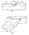
- a MESFET device is shown with substrate 11, typically semi-insulating GaAs, and active layer 12, which is implanted with n-silicon n-type carriers.
- the cap layer 13 for the source/drain contacts is silicon implanted n + .
- the source and drain contacts 14 and 15 are conventional metal materials such as Ti/Pd/Au, Ti/Pt/Au, Al/Ti, Au/Ge.
- the gate is recessed by wet etching a window in layer 13 so that the gate is situated on the active layer 12.
- MESFET devices are typically depletion mode devices with Schottky gates which in contrast with Si MOS transistors are "normally on" devices.
- the Schottky gate for the MESFET device in Fig. 1 is shown at 17, and is made of a conventional contact metal. When reverse biased, n-type carriers are depleted from depletion region 18 beneath the Schottky gate leaving a p-region that pinches off current flow between the source and drain.
- the gate 17 is referred to as T-shaped but is not to be confused with gate configurations, known in the art, that are T-shaped in plan view.
- the gate configuration in Fig. 1, and which describes the objective of the invention, is a vertical T-shape. It can be defined as having a vertical base 21 and a "cross" 22.
- the shape of the gate in a plan view may be square but is conventionally rectangular in shape with the width w of the gate extending into the plane of the figure and typically terminating in a contact pad (not shown) outside the active region of the device.
- Enhancement of the gate conductivity is a function of the increased cross section between the extremities of the gate along the conduction path.
- the important gate dimensions are shown in Fig. 2.
- the objective in these devices is to minimize the gate length l which is the device parameter controlling the frequency response of the transistor.
- the gate length l is reduced to shrink the overall device size the gate resistance along the gate width w increases proportionately.
- the relevant portion of the conduction path i.e. the reduced dimension, extends mainly over the active region from the free end of gate 24 to the gate runner or the contact pad shown generally at 25.
- the contact pad typically is at a different level, i.e. on the field oxide but the levels are omitted for simplicity.
- the enhanced cross section is ( h 2 x l 2 ) - h 1 ( l 2 - l 1 ).
- the gate conductance enhancement factor is 3.
- the gate conductivity is considered enhanced in the context of the invention if the conductance added by the cross of the T-shaped gate contributes an increase of more than 50% to the standard rectangular or square cross sectioned gate. Expressed in terms of the dimensions shown in Fig. 2: ( h 2 x l 2 ) - h 1 ( l 2 - l 1 ) > 1.5 ( l 1 x h 1 )
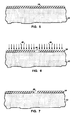
- the two factors that contribute to the enhancement are h 2 /h 1 and l 2 / l 1 . Both must be greater than unity in a T-shaped structure.
- the variation of the enhancement factor with these ratios can be seen in Fig. 3 where the ratio h 2 /h 1 for several values of l 2 / l 1 is plotted vs. enhancement in percent. It is evident that increasing h 2 /h 1 gives relatively diminishing returns when l 2 / l 1 is low, while increasing the length of the cross of the "T", i.e. increasing l 2 / l 1 , is more effective. To obtain an enhancement factor of greater than 50% l 2 / l 1 should be nearly two or greater.
- a HEMT device is shown in Fig. 4. These devices are similar in appearance to the MESFET of Fig. 1 but are more complex in the internal structure and are designed for lower noise, higher frequency performance, and in special structures, higher power.
- the source and drain contacts 31 and 32 are typically formed on an n + GaAs layer 33 but the Schottky gate in this structure contacts a heterostructure layer 34, e.g. AlGaAs, under contact layer 33.
- the active layer 34 and the depletion region 37 are otherwise similar to corresponding elements in the MESFET.
- Layer 38 is a very thin spacer layer of e.g.
- layer 39 is a buffer layer of undoped GaAs.
- the substrate 41 may be semi-insulating GaAs.
- the T-shaped Schottky gate structure is shown at 42 and is essentially the same as in the MESFET device of Fig. 1.
- the technique for fabricating the T-shaped gate structures according to the invention will be described in conjunction with Figs. 5-13.
- the region of the device shown in Figs. 5-13 is the substrate surface between the source and drain electrodes the length of which is exaggerated for illustration.
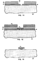
- the substrate 43 is coated with a first level of photoresist 44.
- the choice of photoresist is not critical and can be any conventional resist material, either positive or negative.
- the length and width of photomask feature 46 correspond to the length and width of the base of the T-shaped gate.
- the pattern can then be developed for 20 seconds using Shipley 321 developer, and then rinsed in D.I. water for 30 seconds. After developing the first level of photoresist window 46 remains as shown in Fig. 7.
- the next step is to harden the surface of the first level photoresist so that it can withstand independent patterning of the second level. This is done by exposure to a plasma which, as shown in Fig. 8, creates a surface layer 47 on the first level photoresist which is durable and is insensitive to subsequent lithographic processing.
- the plasma treatment can create this surface layer without excessive damage to the integrity of the underlying photoresist. It also proceeds at a relatively low temperature, i.e. 50-100 °C..
- a recommended apparatus for the plasma treatment is an electron cyclotron resonance system ( 2.45 GHz ) and a recommended plasma gas is nitrogen. Other plasma gases such as argon, xenon, helium, oxygen, etc. may also give acceptable results.
- the preferred gas is an inert gas.
- Suitable flow rate for nitrogen in the ECR reactor is 2-100 sccm and a suitable power level is 20-500 W.
- Treatment time can vary e.g. between 0.5-5 minutes.
- Appropriate plasma processing conditions are highly dependent on the type of plasma reactor used. However plasma treatments are well developed and well understood and the details of the plasma treatment required to render the first level photoresist insensitive to further actinic processing are within the skill of the art. For the purpose of defining this invention the result of the plasma treatment of the first level photoresist is described as rendering the layer lithographically passive.
- the next step in the process is to deposit the second level photoresist 48.
- the second level is then patterned as shown in Fig.10.
- the same procedure can be used as in forming the first photoresist layer except that the mask for the second layer has a larger feature 49 which corresponds to l 2 in Fig. 2.
- the thickness t 2 of the second level photoresist layer 48 corresponds to dimension h 2 of Fig. 2 with an excess height added to accommodate the liftoff process as will be described below.
- the thickness t 2 will typically be in the range 0.3-3.0 mm.
- Shipley 1818 was used for the second level photoresist, and was spun at 3000 rpm for 30 seconds giving a photoresist layer thickness of 1.8 mm.
- the layer was prebaked on a hotplate at 110 °C for 60 seconds.
- the exposure time for the Nikon stepper to expose to the bottom of the second photoresist level was 1200 milliseconds.
- the second level photoresist was developed for 20 seconds in Shipley 321 developer and rinsed in D.I. water for 30 seconds.
- the pattern in the first level photoresist remained intact after patterning the second level.
- the resulting structure, shown in Fig. 11, is then ready for metallization to form the T-shaped gate.
- the deposition technique used to deposit the metal, and the composition of the metal are subject to a variety of choices known to those in the art. Evaporation is preferred because it is relatively directional, and therefore is well suited for lift-off processes. Sputtering may also be used. Conformal coating processes such as Chemical Vapor Deposition (CVD), Molecular Beam Epitaxy (MBE) and Atomic Layer Deposition (ALD), are less likely to be effective but ways may be devised by those skilled in the art to adapt these techniques to the process described. In the specific example described here, the preferred deposition technique is evaporation using an e-beam evaporation process.
- the substrate Prior to evaporation the substrate was exposed to a pre-deposit cleaning operation for 3 minutes in an oxygen plasma at 50 watts and 1 torr, followed by a 20:1 HCl:H 2 O rinse for 30 seconds. The surface was blow dried with nitrogen for 30 seconds.
- a suitable metallization for most applications which is well established in this technology, is 250 Angstroms titanium, 500 Angstroms platinum, and 8000 Angstroms gold. After evaporation of the metal the structure appears as in Fig. 12 with the metallization shown at 51 in the gate region and 52 on the surface of the second level resist. A vertical separation between these metal bodies is intentionally created to facilitate the lift-off process as is well known.
- the excess vertical gap between the top surface of the evaporated metal and the top surface of the second level photoresist was approximately 1.4 mm.
Landscapes
- Junction Field-Effect Transistors (AREA)
- Exposure Of Semiconductors, Excluding Electron Or Ion Beam Exposure (AREA)
Applications Claiming Priority (2)
| Application Number | Priority Date | Filing Date | Title |
|---|---|---|---|
| US935121 | 1997-09-22 | ||
| US08/935,121 US5981319A (en) | 1997-09-22 | 1997-09-22 | Method of forming a T-shaped gate |
Publications (2)
| Publication Number | Publication Date |
|---|---|
| EP0903779A2 true EP0903779A2 (de) | 1999-03-24 |
| EP0903779A3 EP0903779A3 (de) | 2000-11-22 |
Family
ID=25466608
Family Applications (1)
| Application Number | Title | Priority Date | Filing Date |
|---|---|---|---|
| EP98307228A Withdrawn EP0903779A3 (de) | 1997-09-22 | 1998-09-08 | Herstellung von Feldeffekttransistoren |
Country Status (3)
| Country | Link |
|---|---|
| US (1) | US5981319A (de) |
| EP (1) | EP0903779A3 (de) |
| JP (1) | JPH11150130A (de) |
Cited By (2)
| Publication number | Priority date | Publication date | Assignee | Title |
|---|---|---|---|---|
| WO2005081299A3 (en) * | 2004-02-23 | 2006-03-09 | Asml Netherlands Bv | Device manufacturing method and substrate comprising radiation sensitive material |
| CN110429063A (zh) * | 2019-06-28 | 2019-11-08 | 福建省福联集成电路有限公司 | 一种低噪声值的半导体器件制造方法及器件 |
Families Citing this family (14)
| Publication number | Priority date | Publication date | Assignee | Title |
|---|---|---|---|---|
| US7008832B1 (en) | 2000-07-20 | 2006-03-07 | Advanced Micro Devices, Inc. | Damascene process for a T-shaped gate electrode |
| US6403456B1 (en) * | 2000-08-22 | 2002-06-11 | Advanced Micro Devices, Inc. | T or T/Y gate formation using trim etch processing |
| US6355561B1 (en) * | 2000-11-21 | 2002-03-12 | Micron Technology, Inc. | ALD method to improve surface coverage |
| US6541361B2 (en) * | 2001-06-27 | 2003-04-01 | Lam Research Corp. | Plasma enhanced method for increasing silicon-containing photoresist selectivity |
| JP2003142500A (ja) * | 2001-10-30 | 2003-05-16 | Fujitsu Ltd | 半導体装置の製造方法 |
| US6737202B2 (en) * | 2002-02-22 | 2004-05-18 | Motorola, Inc. | Method of fabricating a tiered structure using a multi-layered resist stack and use |
| RU2216818C1 (ru) * | 2003-01-28 | 2003-11-20 | Общество с ограниченной ответственностью "ЭпиЛаб" | Эцр-плазменный источник для обработки полупроводниковых структур, способ обработки полупроводниковых структур, способ изготовления полупроводниковых приборов и интегральных схем (варианты), полупроводниковый прибор или интегральная схема (варианты) |
| US7132372B2 (en) * | 2004-07-29 | 2006-11-07 | Freescale Semiconductor, Inc. | Method for preparing a semiconductor substrate surface for semiconductor device fabrication |
| US7439166B1 (en) | 2005-06-11 | 2008-10-21 | Hrl Laboratories, Llc | Method for producing tiered gate structure devices |
| US7608497B1 (en) | 2006-09-08 | 2009-10-27 | Ivan Milosavljevic | Passivated tiered gate structure transistor and fabrication method |
| US7692222B2 (en) * | 2006-11-07 | 2010-04-06 | Raytheon Company | Atomic layer deposition in the formation of gate structures for III-V semiconductor |
| WO2010109989A1 (ja) | 2009-03-27 | 2010-09-30 | 三菱電機株式会社 | 静電霧化装置及び機器及び空気調和機及び冷蔵庫 |
| CN103700583A (zh) * | 2014-01-06 | 2014-04-02 | 中国科学院微电子研究所 | 一种氮化镓基场效应晶体管的t型栅的制作方法 |
| US9379327B1 (en) * | 2014-12-16 | 2016-06-28 | Carbonics Inc. | Photolithography based fabrication of 3D structures |
Family Cites Families (10)
| Publication number | Priority date | Publication date | Assignee | Title |
|---|---|---|---|---|
| JP2714026B2 (ja) * | 1988-08-30 | 1998-02-16 | 株式会社東芝 | 半導体装置用電極の形成方法 |
| JPH02266535A (ja) * | 1989-04-07 | 1990-10-31 | Sony Corp | 電界効果型半導体装置の製造方法 |
| JPH0590300A (ja) * | 1991-09-30 | 1993-04-09 | Fujitsu Ltd | 半導体装置の製造方法 |
| JP2723405B2 (ja) * | 1991-11-12 | 1998-03-09 | 松下電器産業株式会社 | 微細電極の形成方法 |
| JPH05235055A (ja) * | 1992-02-25 | 1993-09-10 | Sony Corp | 化合物半導体装置 |
| JP2565119B2 (ja) * | 1993-11-30 | 1996-12-18 | 日本電気株式会社 | パターン形成方法 |
| US5693548A (en) * | 1994-12-19 | 1997-12-02 | Electronics And Telecommunications Research Institute | Method for making T-gate of field effect transistor |
| US5776805A (en) * | 1995-12-29 | 1998-07-07 | Lg Semicon Co., Ltd. | Method for manufacturing MESFET |
| TW301061B (en) * | 1996-06-07 | 1997-03-21 | Ind Tech Res Inst | Manufacturing method of submicron T-type gate |
| JP2780704B2 (ja) * | 1996-06-14 | 1998-07-30 | 日本電気株式会社 | 半導体装置の製造方法 |
-
1997
- 1997-09-22 US US08/935,121 patent/US5981319A/en not_active Expired - Lifetime
-
1998
- 1998-09-08 EP EP98307228A patent/EP0903779A3/de not_active Withdrawn
- 1998-09-21 JP JP10267052A patent/JPH11150130A/ja active Pending
Cited By (4)
| Publication number | Priority date | Publication date | Assignee | Title |
|---|---|---|---|---|
| WO2005081299A3 (en) * | 2004-02-23 | 2006-03-09 | Asml Netherlands Bv | Device manufacturing method and substrate comprising radiation sensitive material |
| CN100487867C (zh) * | 2004-02-23 | 2009-05-13 | Asml荷兰有限公司 | 器件制造方法和基片 |
| US7892903B2 (en) | 2004-02-23 | 2011-02-22 | Asml Netherlands B.V. | Device manufacturing method and substrate comprising multiple resist layers |
| CN110429063A (zh) * | 2019-06-28 | 2019-11-08 | 福建省福联集成电路有限公司 | 一种低噪声值的半导体器件制造方法及器件 |
Also Published As
| Publication number | Publication date |
|---|---|
| JPH11150130A (ja) | 1999-06-02 |
| US5981319A (en) | 1999-11-09 |
| EP0903779A3 (de) | 2000-11-22 |
Similar Documents
| Publication | Publication Date | Title |
|---|---|---|
| US6139995A (en) | Method of manufacturing schottky gate transistor utilizing alignment techniques with multiple photoresist layers | |
| US5155053A (en) | Method of forming t-gate structure on microelectronic device substrate | |
| US5981319A (en) | Method of forming a T-shaped gate | |
| US6204102B1 (en) | Method of fabricating compound semiconductor devices using lift-off of insulating film | |
| US5399896A (en) | FET with a T-shaped gate of a particular structure | |
| US5112763A (en) | Process for forming a Schottky barrier gate | |
| EP0810645B1 (de) | Verfahren zur Herstellung eines Heterobipolartransistors mittels zweischichtiger Photolacks | |
| US6294446B1 (en) | Methods of manufacturing a high electron mobility transistor with a T-shaped gate electrode | |
| US5587328A (en) | Method for manufacturing semiconductor device | |
| Chang et al. | Submicron T-shaped gate HEMT fabrication using deep-UV lithography | |
| US5970328A (en) | Fabrication method of T-shaped gate electrode in semiconductor device | |
| US5231040A (en) | Method of making a field effect transistor | |
| US4935377A (en) | Method of fabricating microwave FET having gate with submicron length | |
| US5483089A (en) | Electrically isolated MESFET | |
| Lee et al. | Pseudomorphic AlGaAs/InGaAs/GaAs high electron mobility transistors with super low noise performances of 0.41 dB at 18 GHz | |
| KR19990075338A (ko) | 수도모픽 고 전자 이동도 트랜지스터의 t-게이트 제조 방법 | |
| JPS6341078A (ja) | 半導体装置の製造方法 | |
| EP0613174A2 (de) | Herstellungsverfahren für Halbleiteranordnungen mit feinen Leiterlinien | |
| JPH02285644A (ja) | 半導体装置およびその製造方法 | |
| JPH0684950A (ja) | 電界効果トランジスタの製造方法 | |
| KR100264532B1 (ko) | 모드 또는 문턱전압이 각기 다른 전계효과 트랜지스터 제조 방법 | |
| JP2906856B2 (ja) | 電界効果トランジスタの製造方法 | |
| EP0366939A2 (de) | Verfahren zur Herstellung eines Schottkygitters auf GaAs | |
| JPS62115782A (ja) | 半導体装置の製造方法 | |
| JPH0846146A (ja) | 半導体集積回路の製造方法 |
Legal Events
| Date | Code | Title | Description |
|---|---|---|---|
| PUAI | Public reference made under article 153(3) epc to a published international application that has entered the european phase |
Free format text: ORIGINAL CODE: 0009012 |
|
| AK | Designated contracting states |
Kind code of ref document: A2 Designated state(s): DE FR GB |
|
| AX | Request for extension of the european patent |
Free format text: AL;LT;LV;MK;RO;SI |
|
| PUAL | Search report despatched |
Free format text: ORIGINAL CODE: 0009013 |
|
| AK | Designated contracting states |
Kind code of ref document: A3 Designated state(s): AT BE CH CY DE DK ES FI FR GB GR IE IT LI LU MC NL PT SE |
|
| AX | Request for extension of the european patent |
Free format text: AL;LT;LV;MK;RO;SI |
|
| 17P | Request for examination filed |
Effective date: 20010518 |
|
| AKX | Designation fees paid |
Free format text: DE FR GB |
|
| STAA | Information on the status of an ep patent application or granted ep patent |
Free format text: STATUS: THE APPLICATION IS DEEMED TO BE WITHDRAWN |
|
| 18D | Application deemed to be withdrawn |
Effective date: 20060628 |