EP0968445B1 - Verfahren zur erzeugung einer farbfilterschicht auf einer flachen schirmanzeigestruktur - Google Patents
Verfahren zur erzeugung einer farbfilterschicht auf einer flachen schirmanzeigestrukturInfo
- Publication number
- EP0968445B1 EP0968445B1 EP98905033A EP98905033A EP0968445B1 EP 0968445 B1 EP0968445 B1 EP 0968445B1 EP 98905033 A EP98905033 A EP 98905033A EP 98905033 A EP98905033 A EP 98905033A EP 0968445 B1 EP0968445 B1 EP 0968445B1
- Authority
- EP
- European Patent Office
- Prior art keywords
- color filter
- color
- display screen
- glass substrate
- field emission
- Prior art date
- Legal status (The legal status is an assumption and is not a legal conclusion. Google has not performed a legal analysis and makes no representation as to the accuracy of the status listed.)
- Expired - Lifetime
Links
Images




Classifications
-
- G—PHYSICS
- G02—OPTICS
- G02B—OPTICAL ELEMENTS, SYSTEMS OR APPARATUS
- G02B5/00—Optical elements other than lenses
- G02B5/20—Filters
-
- G—PHYSICS
- G02—OPTICS
- G02B—OPTICAL ELEMENTS, SYSTEMS OR APPARATUS
- G02B5/00—Optical elements other than lenses
- G02B5/20—Filters
- G02B5/201—Filters in the form of arrays
-
- G—PHYSICS
- G03—PHOTOGRAPHY; CINEMATOGRAPHY; ANALOGOUS TECHNIQUES USING WAVES OTHER THAN OPTICAL WAVES; ELECTROGRAPHY; HOLOGRAPHY
- G03F—PHOTOMECHANICAL PRODUCTION OF TEXTURED OR PATTERNED SURFACES, e.g. FOR PRINTING, FOR PROCESSING OF SEMICONDUCTOR DEVICES; MATERIALS THEREFOR; ORIGINALS THEREFOR; APPARATUS SPECIALLY ADAPTED THEREFOR
- G03F7/00—Photomechanical, e.g. photolithographic, production of textured or patterned surfaces, e.g. printing surfaces; Materials therefor, e.g. comprising photoresists; Apparatus specially adapted therefor
- G03F7/0005—Production of optical devices or components in so far as characterised by the lithographic processes or materials used therefor
- G03F7/0007—Filters, e.g. additive colour filters; Components for display devices
Definitions
- the present claimed invention relates to the field of flat panel displays. More particularly, the present claimed invention relates to the fabrication of a color filter layer on a flat panel display screen structure.
- Prior Art Figure 1A illustrates a top view of a black matrix 102 defining a pixel structure.
- Black matrix 102 is disposed on the interior surface of a display screen 100, typically comprised of glass.
- the pixel structure is further divided into sub-pixels, typically shown as 104, of three primary light colors: red (R), green (G), and blue (B).
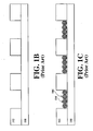
- FIG. 1B A side sectional view of display screen 100 with black matrix 102 disposed on it interior surface is depicted in Prior Art Figure 1B.
- Prior Art Figure 1C illustrates a side sectional view of black matrix 102 disposed on top of display screen 100 with colored phosphors 106 disposed thereon.
- display screen 100 On the interior surface of display screen 100, plurality of sub-pixels 104 are disposed.
- Phosphors 106 are first coated with color pigment crystals 104 of red, green, or blue color. Subsequently, phosphors are put into a slurry consisting of poly vinyl alcohol, a sensitizer (metal dichromate), a dispersant, a surfactant, an emulsifier, a short chain cross linker (TEG), and water. The slurry is spread across the screen.
- the screen is either spun (curved or flat screen) or squeegeed to remove excess slurry after setting for several minutes. It is then-dried. The specific color pixel area is then exposed through a photomask using from side exposure. The excess is then removed using a water solution.
- phosphors 106 coated with color pigment crystals 108 are then cured into corresponding pixels on the interior surface by an ultraviolet (UV) light 108 illuminated from the interior side of the display screen 100.
- UV ultraviolet
- a photomask is used to ensure curing of color pigment crystals in desired sub-pixels only. That is, the material must not be cured along the top or the edge of black matrix 102.
- a side sectional view of another display screen 100 is illustrated.
- a black matrix 102 defining a plurality of sub-pixels corresponding to red, green, and blue colors is disposed.
- phosphors are put into a slurry consisting of poly-vinyl alcohol, a sensitizer (metal dichromate), a dispersant, a surfactant, an emulsifier, a short chain cross linker (TEG), and water.
- the slurry is spread across the screen.
- the screen is either spun (curved or flat screen) or squeegeed to remove excess slurry after setting for several minutes. It is then dried.
- the specific color pixel area is then exposed through a photomask using from side exposure. The excess is then removed using a water solution.
- the color crystal pigments 104 are then cured into the pixels on the interior surface by UV light 108 illuminated from the interior side of the display screen 100.
- Phosphors are then deposited into the sub-pixels on top of the color crystal pigments by a well known photolithographic process.
- a photomask is used to ensure curing of color pigment crystals in desired sub-pixels only. That is, the material must not be cured along the top or the edge of black matrix 102.
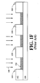
- Prior Art Figure 1F illustrates portions 109 of color pigment crystals 104 on top of black matrix 102, which should not be cured.
- cross-linking of color pigment crystals means that the exposure to an UV light must proceed at a relatively slow pace. That is, rapid exposure to UV light enhances the detrimental cross-linking effect at the top of the layer of color pigment crystals.
- the present invention provides a method for fabricating a color filter on a display screen which improves readability of display screens by reducing reflection of ambient light and by increasing transmission of phosphor light of desired wavelength with minimal reduction in overall screen efficiency.
- the present invention further provides a method for achieving the above-mentioned color filter in a way that provides a more efficient adhesion of color pigment crystals to the screen display structure while decreasing the need for high precision alignment thereby decreasing equipment cost.
- the present invention creates a color filter on a glass substrate having a pixel-defining structure.
- the present embodiment first creates a color filter slurry by mixing poly vinyl alcohol, a sensitizer (metal dichromate), a dispersant, a surfactant, an emulsifier, a short chain cross linker (TEG), and water.
- the color filter slurry is then applied onto the interior surface of the display screen.
- the slurry is then dried.
- the dried color filter slurry is then exposed to an UV light from the exterior side of the display screen using a slotted photomask instead of pixelated photomask.
- the UV light exposes the color filter slurry through a photomask and through the display screen.
- the excess layer of color filter slurry is then removed, leaving behind a cured color filter of desired transmission wavelength. In doing so, light having a similar wavelength is substantially transmitted through the display screen. Similarly, light having a different wavelength than the color pigment crystals is substantially filtered out by absorption.
- a color filter is created on a glass substrate having a pixel structure defining black matrix with sub-pixels of red, green, and blue colors.
- the color filter in this embodiment is achieved by first creating a color filter slurry by mixing a polyvinyl alcohol solution with a color crystal pigment of red, green, or blue. Each color filter slurry corresponds to the sub-pixel colors of red, green, and blue.
- the color filter slurry is then applied onto the interior surface of the display screen.
- the slurry is then dried.
- the dried color filter slurry is then exposed to a light from the exterior side of the display screen. The light exposes the color filter slurry through a photomask and through the display screen.
- the present invention provides a method for fabricating a color filter on a display screen which improves readability of display screens by reducing reflection of ambient light in a way that provides a more efficient adhesion of color pigment crystals to the screen display structure while improving decreasing the need for tolerancing in the photolithography process.
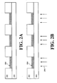
- FIG. 2A of the present embodiment a side sectional view of a glass substrate 200 having a black matrix 202 is illustrated.
- Use of glass as display screen material is well known in the art. However, those of ordinary skill in the art will appreciate that use of other transparent materials may also be suitable to the present invention.
- a black matrix 202 is disposed on the interior surface of a glass substrate 200 and defines a pixel structure on display screen 200.
- the use of a black matrix in the field of flat panel display structures is well known in the art. However, those skilled in the art will appreciate that use of other pixel-defining structures are also suitable to the present invention.
- black matrix 202 of the present embodiment is disposed on the interior side of glass substrate 200.
- Black matrix 202 comprises walls defining a plurality of wells therein. These wells, in turn, define the pixel structure in the present embodiment.
- the present invention creates fine color pigment crystals which will serve as a color filter material.
- these pigment crystals are ball-milled into fine crystals of nanocrystalline size. Ball-milling is a method well known in the art for obtaining nanocrystalline sizes. However, those skilled in the art will appreciate that other methods can be used to obtain fine crystalline sizes.
- the color pigment crystals are chosen from a group consisting of cobalt aluminate, iron oxide, and chromium oxide.
- Such color pigments include, for example, Harshaw #7546 for blue, Harshaw #9384 for red, and Harshaw #3955 or #9440 for green, all of which are manufactured by the Englehard Corporation of Cleveland, Ohio.
- These materials are chosen in the present embodiment because their color filter characteristics correspond to the three primary colors of light: cobalt aluminate for blue, iron oxide for red, and chromium oxide for green.
- these color pigment crystals exhibit filter characteristics centered around their characteristic wavelengths.
- chromium oxide exhibits a characteristic wavelength of green color light.
- chromium oxide crystals transmit green color light while absorbing light of other colors or wavelengths. Hence, these crystals in effect "filter” out light of unwanted color or wavelength.
- color pigment crystal materials are used in the present embodiment, the present invention is also well suited for use with various other color materials.
- the present invention then mixes the color pigment crystals with a polyvinyl alcohol solution to create a color filter slurry.
- the polyvinyl alcohol solution comprises 5% by volume of polyvinyl alcohol, 0.2 to 5% by weight of metal dichromate, a surfactant, a dispersant, an emulsifier, tetraethylene glycol, 2.5% by volume metal acetate buffer, and water for the balance.
- the present embodiment then applies a layer of the color filter slurry onto the interior side of the glass substrate.
- This color filter slurry is allowed to settle into the pixels as defined by the wells of black matrix.
- color filter slurries are applied sequentially, one at a time, from application onto the glass substrate, through UV light exposure, to removal of excess slurries.
- the present embodiment repeats the entire process from beginning to end, for each color. For example, to form a color filter for red pixels, the red color filter slurry is applied onto the glass substrate. Then, the red color slurry is cured by UV light. Finally, the red color slurry in unwanted pixel areas are removed.
- the entire process repeats until all three color pigment crystals of red, green, and blue have been deposited and cured.
- the color filter slurries are applied by screen printing or squeeging process, which is well known in the art. However, those with ordinary skill in the art will appreciate that other methods of application are also suitable for the present invention.
- the present invention applies all color slurries, one color after another before proceeding to the next step. For example, a red color slurry is applied. Then, a green color slurry is deposited. Finally, a blue color slurry is applied. Then, all three color slurries are exposed onto the pixel areas at the same time.
- the present embodiment uses a pixelated metal to mask unwanted pixel areas. Then all color filter slurries are sprayed or screen printed one by one using a separate pixelated metal mask for each color. Hence, all color slurries will be deposited into pixels of corresponding colors. Screen and spray printing and photomasking are well known in the art. Those with ordinary skill in the art, however, will appreciate that other methods of applying and masking are also suitable for the present invention.
- the present invention then dries the color filter slurry.
- the excess slurry is squeegeed off and the color filter slurry is dried and then exposed. Even though a squeeging process is used in the present embodiment, those having ordinary skill in the art will no doubt appreciate other methods of removing excess slurries.
- the present embodiment then exposes the layer of the dried color filter slurry to an UV light 206 from the exterior side of the glass substrate 200.
- the use of UV light for effecting a cure is well known in the art. However, those skilled in the art will appreciate that other light may be used for exposing the dried color filter slurry.
- the UV light exposure takes place through glass substrate 200 and through a photomask.
- the thickness of glass substrate 200 is about 1.1 mm (e.g., Shot D623 glass). It is well known in the art that a thin glass, such as Shot D623, has excellent UV properties. However, those skilled in the art will appreciate that other transparent materials of differing thickness with excellent UV properties may be suitable to the present invention.
- a photomask is used to enable exposure of predetermined pixels only.
- the photomask is used to expose only the color pigment crystals located in desired color pixels. For instance, the photomask exposes red color pigment crystals disposed within the pixels having a preassigned color of red. Similarly, the photomask enables exposure only of pixels with a preassigned color of green.
- the present invention then removes excess layer of the exposed color filter slurry by, for example, squeegeeing, leaving a color filter of desired color transmission wavelength disposed on the glass substrate.
- the excess layer of exposed color filter slurry is formed on top of pixels having preassigned colors that are different from the color of the color filter slurry.
- the unwanted layer may be removed by either washing it off or baking it off.
- Those skilled in the art are readily familiar with these exemplary removal methods. However, they will appreciate that other removal methods may be equally suitable for the present invention.
- the present embodiment exposes the color filter slurry through glass substrate 200 as shown in Figure 2B.
- the dried color slurry contacting glass substrate 200 is exposed first.
- the color pigment crystals 204 solidly adhere to glass substrate 200 during the exposure process.
- Preventing rapid exposure at a low pH prevents "deep" crosslinking.
- a neutral pH of 6-8 is required for this, otherwise, exposure at a pH below 6 rapidly decreases the transmission spectra.
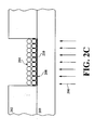
- the exposure process of the present embodiment is generally illustrated in Figure 2B and more particularly depicted in Figure 2C.
- color pigment crystals 204 form a layer of color filter on the interior surface of glass substrate 200.
- Color pigment crystals 204 are exposed to UV light 206.
- the color pigment crystals 204 upon being exposed to UV light 206, the color pigment crystals 204 in direct contact with glass substrate 200 contact bond 208 with the surface of glass substrate 200.
- the color pigment crystals 204 also cross-link, as shown by structure 210, to other adjacent crystals. As a result, color pigment crystals 204 form a more adhesive and coherent layer in the present embodiment.
- the present invention advantageously utilizes the black matrix as a built-in mask.
- the conventional method of exposing the crystals from the top side of a black matrix required extreme precision in the alignment of a photomask.
- a misalignment meant curing of unwanted color pigment crystals on top or edges of a black matrix.
- UV light 206 exposes color pigment crystals 204 from the bottom side of black matrix 202, i.e. the interior side of glass substrate 200.
- the present invention uses black matrix 202 as a natural mask to prevent curing of unwanted color pigment crystals on to top or edges of black matrix. As a result, a minor misalignment of a photomask does not produce curing of color pigment crystals at unwanted areas.
- the present invention has other advantages.
- the present embodiment shows a layer of phosphors 212 disposed on top of the color pigment crystals. Unlike some conventional phosphors, the phosphors in the present invention need not be coated with color crystals.
- Figure 2E illustrates how color pigment crystals function as a color filter.
- Light 216 originating from outside and entering the pixel area is intercepted by color pigment crystals 204.
- Visible light is usually comprised of all wavelengths in the visible light spectrum.
- Light 216 having wavelengths different from color pigment crystals 204 is absorbed while light 215 having a similar wavelength to the color pigment crystals 204 is reflected by the filter.
- unwanted reflection off the display screen is substantially reduced.
- light 214 originating from phosphors 212 has a similar wavelength characteristic to the color pigment crystals.
- phosphor light is substantially transmitted through the filter to the viewing screen.
- the color crystal filter of the present embodiment can make the colors more saturated at the desired transmission wavelength.
- the present invention provides a method for fabricating a color filter on a display screen which improves readability of display screens by reducing reflection of ambient light and by increasing transmission of phosphor light of desired wavelength without much reduction in transmission of light by the phosphors in a way that provides a more efficient adhesion of color pigment crystals to the screen display structure while decreasing the need for high precision alignment thereby decreasing equipment cost.
Landscapes
- Physics & Mathematics (AREA)
- General Physics & Mathematics (AREA)
- Optics & Photonics (AREA)
- Optical Filters (AREA)
- Cathode-Ray Tubes And Fluorescent Screens For Display (AREA)
- Devices For Indicating Variable Information By Combining Individual Elements (AREA)
- Formation Of Various Coating Films On Cathode Ray Tubes And Lamps (AREA)
Claims (11)
- Verfahren zum Härten oder Erzeugen eines Farbfilters auf einem Feldemissionsbildschirm, welches Verfahren die Schritte umfasst:a) Aufbringen einer Farbfilter-Aufschlämmung auf eine Oberfläche eines Glassubstrats des Feldemissionsbildschirms, um eine Lage einer Farbfilter-Aufschlämmung zu erzeugen;b) Trocknen der Lage der Farbfilter-Aufschlämmung; undc) Exponieren der Lage der Farbfilter-Aufschlämmung an UV-Licht von oder durch die Außenseite des Glassubstrats des Feldemissionsbildschirms hindurch, sodass die Farbfilter-Aufschlämmung härtet und an der Innenseite des Glassubstrats haftet oder mit ihr klebend verbunden ist.
- Verfahren nach Anspruch 1, bei welchem in Schritt a) die Farbfilter-Aufschlämmung in Pixelbereichen eingebracht wird, die auf der Innenseite des Glases angeordnet sind, wobei die Pixelbereiche durch eine Black-Matrixstruktur festgelegt sind und wobei Schritt a) ferner den Schritt umfasst:Einbringen einer Farbfilter-Aufschlämmung in die Pixelbereiche, die auf der Innenseite des Glassubstrats angeordnet sind, wobei die Farbfilter-Aufschlämmung aufweist:5 Vol.% Polyvinylalkohol,0,2% bis 5 Gew.% Metalldichromat,ein Tensid,ein Dispergiermittel,ein Emulgiermittel,Tetraethylenglykol,2,5 Vol% Metallacetat-Puffer undWasser.
- Verfahren nach Anspruch 1 oder 2, wobei Schritt c) ferner das Exponieren der Lage der Farbfilter-Aufschlämmung an UV-Licht von der Außenseite des Glassubstrats des Feldemissionsbildschirms umfasst, sodass eine/die Black-Matrixstruktur Abschnitte der Farbfilter-Aufschlämmung gegenüber dem UV-Licht maskiert.
- Verfahren nach Anspruch 1, bei welchem der Feldemissionsbildschirm eine darauf ausgebildete Black-Matrixstruktur hat, wobei die Black-Matrixstruktur Farb-Subpixel festlegt, und worin in dem Schritt des Aufbringens das Farbfilter eine erste Farbfilter-Aufschlämmung ist, die in die Pixelbereiche hinein eingetragen wird, die auf der Innenseite des Glassubstrats des Feldemissionsbildschirms angeordnet sind und wobei die Pixelbereiche durch die Black-Matrixstruktur festgelegt sind; wobei das Verfahren ferner die Schritte umfasst:Entfernen überschüssiger Anteile der ersten Lage der Farbfilter-Aufschlämmung, sodass die erste Lage der Farbaufschlämmung lediglich in ausgewählten entsprechenden, ersten Farb-Subpixeln verbleibt, undWiederholen der vorangegangenen Schritte für die entsprechenden zweiten und dritten Farbfilter-Aufschlämmungen.
- Verfahren nach Anspruch 4, wobei Schritt a) ferner den Schritt umfasst:Einbringen einer ersten Farbfilter-Aufschlämmung in die Pixelbereiche, die auf der Innenseite des Glassubstrats angeordnet sind, wobei die erste Farbfilter-Aufschlämmung aufweist:5 Vol.% Polyvinylalkohol,0,2% bis 5Gew.% Metalldichromat,ein Tensid,ein Dispergiermittel,ein Emulgiermittel,Tetraethylenglykol,2,5 Vol% Metallacetat-Puffer undWasser.
- Verfahren nach einem der vorgenannten Ansprüche, wobei Schritt a) ferner den Schritt umfasst:Aufbringen einer Farbfilter-Aufschlämmung die Farbpigmentkristalle aus der Gruppe enthält, bestehend aus Cobaltaluminat, Eisenoxid und Chromoxid in die Pixelbereiche, die auf der Innenseite des Glassubstrats des Feldemissionsbildschirms angeordnet sind.
- Verfahren nach einem der vorgenannten Ansprüche, wobei Schritt a) ferner das Aufbringen der Farbfilter-Aufschlämmung in die Pixelbereiche umfasst, wobei die Pixelbereiche durch eine/die Black-Matrixstruktur festgelegt sind.
- Verfahren nach einem der vorgenannten Ansprüche, worin Schritt c) ferner das Verwenden einer Fotomaske zur Exponierung der ersten Lage der Farbfilter-Aufschlämmung an UV-Licht von der Außenseite des Glassubstrats des Feldemissionsbildschirms umfasst, so das lediglich ausgewählte Pixelbereiche, die die erste Farbfilter-Aufschlämmung enthalten, an dem UV-Licht exponiert werden.
- Verfahren zum Erzeugen eines Farbfilters auf einem Feldemissionsbildschirm mit einer darauf ausgebildeten Black-Matrixstruktur, wobei die Black-Matrixstruktur Farb-Subpixel festlegt und wobei das Verfahren die Schritte umfasst:a) Abscheiden einer ersten Farbfilter-Aufschlämmung in die ausgewählten ersten Farb-Subpixel, die auf der Innenseite eines Glassubstrats des Feldemissionsbildschirms angeordnet sind,b) Abscheiden einer zweiten Farbfilter-Aufschlämmung in die zweiten Farb-Subpixel, die auf der Innenseite des Glassubstrats des Feldemissionsbildschirms angeordnet sind,c) Abscheiden einer dritten Farbfilter-Aufschlämmung in die dritten Farb-Subpixel, die auf der Innenseite des Glassubstrats des Feldemissionsbildschirms angeordnet sind,d) Trocknen der ersten, zweiten und dritten Farbfilter-Aufschlämmungen,e) Exponieren der ersten, zweiten und dritten Farbfilter-Aufschlämmung an UV-Licht durch die Außenseite des Glassubstrats des Feldemissionsbildschirms hindurch, so das die ersten, zweiten und dritten Farbfilter-Aufschlämmungen gehärtet und an der Innenseite des Glassubstrats des Feldemissionsbildschirms klebend gebunden werden.
- Verfahren nach Anspruch 9, wobei die Schritte a) bis c) ferner die Schritte umfassen:Aufbringen einer ersten Farbfilter-Aufschlämmung, die Farbpigmentkristalle enthält, die die Gruppe aufweisen, bestehend aus Cobaltaluminat, Eisenoxid und Chromoxid, in die ersten Farb-Subpixel hinein, die auf der Innenseite des Glassubstrats des Feldemissionsbildschirms angeordnet sind,Aufbringen einer zweiten Farbfilter-Aufschlämmung, die Farbpigmentkristalle enthält, die die Gruppe aufweisen, bestehend aus Cobaltaluminat, Eisenoxid und Chromoxid, in die zweiten Farb-Subpixel, die auf der Innenseite des Glassubstrats des Feldemissionsbildschirms angeordnet sind, undAufbringen einer dritten Farbfilter-Aufschlämmung, die Farbpigmentkristalle enthält, die die Gruppe aufweisen, bestehend aus Cobaltaluminat, Eisenoxid und Chromoxid, in die dritten Farb-Subpixel hinein, die auf der Innenseite des Glassubstrats des Feldemissionsbildschirms angeordnet sind.
- Verfahren nach Anspruch 9 oder 10, wobei Schritt c) ferner das Exponieren der Lage der Farbfilter-Aufschlämmung an UV-Licht von der Außenseite des Glassubstrats des Feldemissionsbildschirms umfasst, so das die Black-Matrixstruktur unerwünschte Abschnitte der ersten, zweiten und dritten Farbfilter-Aufschlämmungen davor maskiert, von dem UV-Licht exponiert zu werden.
Applications Claiming Priority (3)
| Application Number | Priority Date | Filing Date | Title |
|---|---|---|---|
| US08/807,440 US6025097A (en) | 1997-02-28 | 1997-02-28 | Method for creating a color filter layer on a field emission display screen structure |
| US807440 | 1997-02-28 | ||
| PCT/US1998/002570 WO1998038535A1 (en) | 1997-02-28 | 1998-02-10 | Method for creating a color filter layer on a flat panel display screen structure |
Publications (3)
| Publication Number | Publication Date |
|---|---|
| EP0968445A1 EP0968445A1 (de) | 2000-01-05 |
| EP0968445A4 EP0968445A4 (de) | 2005-07-13 |
| EP0968445B1 true EP0968445B1 (de) | 2006-08-16 |
Family
ID=25196375
Family Applications (1)
| Application Number | Title | Priority Date | Filing Date |
|---|---|---|---|
| EP98905033A Expired - Lifetime EP0968445B1 (de) | 1997-02-28 | 1998-02-10 | Verfahren zur erzeugung einer farbfilterschicht auf einer flachen schirmanzeigestruktur |
Country Status (6)
| Country | Link |
|---|---|
| US (1) | US6025097A (de) |
| EP (1) | EP0968445B1 (de) |
| JP (1) | JP2001504250A (de) |
| KR (1) | KR20000070618A (de) |
| DE (1) | DE69835587T2 (de) |
| WO (1) | WO1998038535A1 (de) |
Families Citing this family (18)
| Publication number | Priority date | Publication date | Assignee | Title |
|---|---|---|---|---|
| US6322937B1 (en) * | 1997-02-28 | 2001-11-27 | Candescent Technologies Corporation | Method for creating a color filter layer on a field emission display screen structure |
| US6760086B2 (en) * | 1998-03-26 | 2004-07-06 | Tomoegawa Paper Co., Ltd. | Attachment film for electronic display device |
| US6620012B1 (en) * | 2000-10-27 | 2003-09-16 | Science Applications International Corporation | Method for testing a light-emitting panel and the components therein |
| US6796867B2 (en) * | 2000-10-27 | 2004-09-28 | Science Applications International Corporation | Use of printing and other technology for micro-component placement |
| US6545422B1 (en) * | 2000-10-27 | 2003-04-08 | Science Applications International Corporation | Socket for use with a micro-component in a light-emitting panel |
| US7288014B1 (en) | 2000-10-27 | 2007-10-30 | Science Applications International Corporation | Design, fabrication, testing, and conditioning of micro-components for use in a light-emitting panel |
| US6570335B1 (en) | 2000-10-27 | 2003-05-27 | Science Applications International Corporation | Method and system for energizing a micro-component in a light-emitting panel |
| US6764367B2 (en) * | 2000-10-27 | 2004-07-20 | Science Applications International Corporation | Liquid manufacturing processes for panel layer fabrication |
| US6612889B1 (en) | 2000-10-27 | 2003-09-02 | Science Applications International Corporation | Method for making a light-emitting panel |
| US6822626B2 (en) | 2000-10-27 | 2004-11-23 | Science Applications International Corporation | Design, fabrication, testing, and conditioning of micro-components for use in a light-emitting panel |
| US6935913B2 (en) * | 2000-10-27 | 2005-08-30 | Science Applications International Corporation | Method for on-line testing of a light emitting panel |
| US6762566B1 (en) | 2000-10-27 | 2004-07-13 | Science Applications International Corporation | Micro-component for use in a light-emitting panel |
| US6801001B2 (en) * | 2000-10-27 | 2004-10-05 | Science Applications International Corporation | Method and apparatus for addressing micro-components in a plasma display panel |
| US20050189164A1 (en) * | 2004-02-26 | 2005-09-01 | Chang Chi L. | Speaker enclosure having outer flared tube |
| KR100738257B1 (ko) * | 2006-01-03 | 2007-07-12 | (주)실리콘화일 | 컬러필터가 형성된 이미지센서 및 그 제조 방법 |
| KR20080099732A (ko) | 2007-05-10 | 2008-11-13 | 연세대학교 산학협력단 | 전자 종이 디스플레이 및 이의 제조방법 |
| CN104575281B (zh) * | 2013-10-21 | 2018-03-20 | 成程投资集团有限责任公司 | 一种显示屏及显示装置 |
| CN113895132B (zh) * | 2021-09-01 | 2023-09-22 | 中光科技(福建)有限公司 | 安防调度指挥系统用触摸屏玻璃基板生产线组 |
Family Cites Families (16)
| Publication number | Priority date | Publication date | Assignee | Title |
|---|---|---|---|---|
| US4392077A (en) * | 1979-02-14 | 1983-07-05 | Zenith Radio Corporation | Deeply filtered television image display |
| US4878741A (en) * | 1986-09-10 | 1989-11-07 | Manchester R & D Partnership | Liquid crystal color display and method |
| JP2587653B2 (ja) * | 1987-09-24 | 1997-03-05 | 富士写真フイルム株式会社 | カラーフィルターの製造方法 |
| US5212575A (en) * | 1988-08-30 | 1993-05-18 | Canon Kabushiki Kaisha | Functional substrate for controlling pixels |
| JPH05241014A (ja) * | 1992-02-27 | 1993-09-21 | Stanley Electric Co Ltd | カラーフィルタの製造方法 |
| JP3297929B2 (ja) * | 1992-03-25 | 2002-07-02 | ソニー株式会社 | 陰極線管の蛍光面の形成方法 |
| JPH05275007A (ja) * | 1992-03-25 | 1993-10-22 | Sony Corp | 陰極線管の蛍光面形成方法 |
| EP0623944B1 (de) * | 1993-05-05 | 1997-07-02 | AT&T Corp. | Flache Bildwiedergabeanordnung und Herstellungsverfahren |
| US5606462A (en) * | 1993-07-12 | 1997-02-25 | Futaba Denshi Kogyo K.K. | Color filter and fluorescent display device having color filters incorporated therein |
| JPH07294722A (ja) * | 1994-04-28 | 1995-11-10 | Toppan Printing Co Ltd | カラーフィルタの製造方法 |
| JPH0829615A (ja) * | 1994-07-14 | 1996-02-02 | Sony Corp | パターンの修正方法 |
| JPH0895024A (ja) * | 1994-09-28 | 1996-04-12 | Canon Inc | カラーフィルター、その製造方法、及び同カラーフィルターを組込んだ液晶表示パネル |
| DE69507874T2 (de) * | 1994-12-26 | 1999-07-29 | Kabushiki Kaisha Toshiba, Kawasaki, Kanagawa | Bildschirm und Verfahren zur Herstellung desselben |
| JPH0954209A (ja) * | 1995-08-18 | 1997-02-25 | Seikosha Co Ltd | カラーフィルタの形成方法 |
| JPH10111506A (ja) * | 1996-10-07 | 1998-04-28 | Dainippon Printing Co Ltd | カラーフィルタおよびその製造方法 |
| JP3227395B2 (ja) * | 1996-10-29 | 2001-11-12 | シャープ株式会社 | カラーフィルターの製造方法 |
-
1997
- 1997-02-28 US US08/807,440 patent/US6025097A/en not_active Expired - Lifetime
-
1998
- 1998-02-10 KR KR1019997006866A patent/KR20000070618A/ko not_active Ceased
- 1998-02-10 DE DE69835587T patent/DE69835587T2/de not_active Expired - Lifetime
- 1998-02-10 EP EP98905033A patent/EP0968445B1/de not_active Expired - Lifetime
- 1998-02-10 WO PCT/US1998/002570 patent/WO1998038535A1/en not_active Ceased
- 1998-02-10 JP JP53767798A patent/JP2001504250A/ja active Pending
Also Published As
| Publication number | Publication date |
|---|---|
| DE69835587T2 (de) | 2007-08-16 |
| JP2001504250A (ja) | 2001-03-27 |
| WO1998038535A1 (en) | 1998-09-03 |
| EP0968445A4 (de) | 2005-07-13 |
| US6025097A (en) | 2000-02-15 |
| DE69835587D1 (de) | 2006-09-28 |
| EP0968445A1 (de) | 2000-01-05 |
| KR20000070618A (ko) | 2000-11-25 |
Similar Documents
| Publication | Publication Date | Title |
|---|---|---|
| US6025097A (en) | Method for creating a color filter layer on a field emission display screen structure | |
| EP0740183B1 (de) | Zusammensetzung für eine Schwarzmatrix, Herstellung einer Schwarzmatrix und Gegenstand mit einer solchen Matrix | |
| US4626071A (en) | Optical filter made of inorganic material for red light | |
| US5914558A (en) | Cathode ray tube with color filters aligned with phosphors | |
| EP0166371B1 (de) | Optischer Filter aus inorganischem Material für grünes Licht | |
| US3884695A (en) | Process for fabricating a color cathode ray tube screen structure having superimposed optical filter means therein | |
| US6322937B1 (en) | Method for creating a color filter layer on a field emission display screen structure | |
| US6482556B1 (en) | Thermosensible transfer film and method of using the same | |
| US7595585B2 (en) | Color conversion and optical enhancement layers for electroluminescent displays | |
| US5009972A (en) | Blank plates for forming multi-color fluorescent planes and methods for forming multi-color fluorescent planes | |
| US5846677A (en) | Color filter, color filter-equipped display device and method for manufacturing same | |
| JPH09134686A (ja) | 画像表示装置 | |
| JPH05275008A (ja) | 赤色フィルタの形成方法、並びに陰極線管の蛍光面用の赤色フィルタの形成方法、並びに陰極線管の蛍光面用の3色フィルタの形成方法 | |
| US4331752A (en) | Method of forming fluorescent screens of color picture tubes | |
| EP0739024B1 (de) | Verfahren zur Bildung eines fluoreszenten Films einer Farbröhre | |
| KR100263860B1 (ko) | 적색 필터막 형성방법 | |
| JPH04277439A (ja) | プラズマディスプレイパネル及びその製造方法 | |
| KR20000017222A (ko) | 디스플레이용 형광면의 형성방법 | |
| JPH07179711A (ja) | 顔料分散液組成物、フィルター付き蛍光膜を有する表示装置及びフィルター付き蛍光膜を有する表示装置の製造方法 | |
| JP4345159B2 (ja) | カラー液晶ディスプレー | |
| KR100363800B1 (ko) | 플라즈마 디스플레이 패널의 배면판 제조방법 | |
| US20050194882A1 (en) | Color cathode ray tube with optical filter system | |
| JP2732251B2 (ja) | 多色螢光面形成方法 | |
| JPH0447640A (ja) | カラー放電表示パネルおよびその製造方法 | |
| KR20000001582A (ko) | 배면노광방식을 이용한 형광면 제조방법 |
Legal Events
| Date | Code | Title | Description |
|---|---|---|---|
| PUAI | Public reference made under article 153(3) epc to a published international application that has entered the european phase |
Free format text: ORIGINAL CODE: 0009012 |
|
| 17P | Request for examination filed |
Effective date: 19990922 |
|
| AK | Designated contracting states |
Kind code of ref document: A1 Designated state(s): DE FR GB |
|
| RIN1 | Information on inventor provided before grant (corrected) |
Inventor name: DRUMM, PAUL, M. |
|
| RAP1 | Party data changed (applicant data changed or rights of an application transferred) |
Owner name: CANDESCENT INTELLECTUAL PROPERTY SERVICES, INC. |
|
| 111L | Licence recorded |
Free format text: 20010911 0100 CANDESCENT TECHNOLOGIES CORPORATION |
|
| A4 | Supplementary search report drawn up and despatched |
Effective date: 20050527 |
|
| RIC1 | Information provided on ipc code assigned before grant |
Ipc: 7G 02B 5/20 B Ipc: 7H 01J 29/32 B Ipc: 7G 03F 7/00 A |
|
| GRAP | Despatch of communication of intention to grant a patent |
Free format text: ORIGINAL CODE: EPIDOSNIGR1 |
|
| GRAS | Grant fee paid |
Free format text: ORIGINAL CODE: EPIDOSNIGR3 |
|
| GRAA | (expected) grant |
Free format text: ORIGINAL CODE: 0009210 |
|
| AK | Designated contracting states |
Kind code of ref document: B1 Designated state(s): DE FR GB |
|
| REG | Reference to a national code |
Ref country code: GB Ref legal event code: FG4D |
|
| REF | Corresponds to: |
Ref document number: 69835587 Country of ref document: DE Date of ref document: 20060928 Kind code of ref document: P |
|
| ET | Fr: translation filed | ||
| REG | Reference to a national code |
Ref country code: GB Ref legal event code: 732E |
|
| PLBE | No opposition filed within time limit |
Free format text: ORIGINAL CODE: 0009261 |
|
| STAA | Information on the status of an ep patent application or granted ep patent |
Free format text: STATUS: NO OPPOSITION FILED WITHIN TIME LIMIT |
|
| 26N | No opposition filed |
Effective date: 20070518 |
|
| REG | Reference to a national code |
Ref country code: FR Ref legal event code: TP |
|
| PGFP | Annual fee paid to national office [announced via postgrant information from national office to epo] |
Ref country code: GB Payment date: 20130220 Year of fee payment: 16 Ref country code: FR Payment date: 20130315 Year of fee payment: 16 Ref country code: DE Payment date: 20130228 Year of fee payment: 16 |
|
| REG | Reference to a national code |
Ref country code: DE Ref legal event code: R119 Ref document number: 69835587 Country of ref document: DE |
|
| GBPC | Gb: european patent ceased through non-payment of renewal fee |
Effective date: 20140210 |
|
| REG | Reference to a national code |
Ref country code: FR Ref legal event code: ST Effective date: 20141031 |
|
| REG | Reference to a national code |
Ref country code: DE Ref legal event code: R119 Ref document number: 69835587 Country of ref document: DE Effective date: 20140902 |
|
| PG25 | Lapsed in a contracting state [announced via postgrant information from national office to epo] |
Ref country code: GB Free format text: LAPSE BECAUSE OF NON-PAYMENT OF DUE FEES Effective date: 20140210 Ref country code: DE Free format text: LAPSE BECAUSE OF NON-PAYMENT OF DUE FEES Effective date: 20140902 Ref country code: FR Free format text: LAPSE BECAUSE OF NON-PAYMENT OF DUE FEES Effective date: 20140228 |