EP0967657A2 - NMOS-Transistor - Google Patents
NMOS-Transistor Download PDFInfo
- Publication number
- EP0967657A2 EP0967657A2 EP99112269A EP99112269A EP0967657A2 EP 0967657 A2 EP0967657 A2 EP 0967657A2 EP 99112269 A EP99112269 A EP 99112269A EP 99112269 A EP99112269 A EP 99112269A EP 0967657 A2 EP0967657 A2 EP 0967657A2
- Authority
- EP
- European Patent Office
- Prior art keywords
- region
- substrate
- well
- type region
- nmos transistor
- Prior art date
- Legal status (The legal status is an assumption and is not a legal conclusion. Google has not performed a legal analysis and makes no representation as to the accuracy of the status listed.)
- Granted
Links
Images


Classifications
-
- H—ELECTRICITY
- H10—SEMICONDUCTOR DEVICES; ELECTRIC SOLID-STATE DEVICES NOT OTHERWISE PROVIDED FOR
- H10D—INORGANIC ELECTRIC SEMICONDUCTOR DEVICES
- H10D62/00—Semiconductor bodies, or regions thereof, of devices having potential barriers
- H10D62/10—Shapes, relative sizes or dispositions of the regions of the semiconductor bodies; Shapes of the semiconductor bodies
- H10D62/13—Semiconductor regions connected to electrodes carrying current to be rectified, amplified or switched, e.g. source or drain regions
- H10D62/149—Source or drain regions of field-effect devices
- H10D62/151—Source or drain regions of field-effect devices of IGFETs
-
- H—ELECTRICITY
- H10—SEMICONDUCTOR DEVICES; ELECTRIC SOLID-STATE DEVICES NOT OTHERWISE PROVIDED FOR
- H10D—INORGANIC ELECTRIC SEMICONDUCTOR DEVICES
- H10D62/00—Semiconductor bodies, or regions thereof, of devices having potential barriers
- H10D62/10—Shapes, relative sizes or dispositions of the regions of the semiconductor bodies; Shapes of the semiconductor bodies
- H10D62/124—Shapes, relative sizes or dispositions of the regions of semiconductor bodies or of junctions between the regions
- H10D62/126—Top-view geometrical layouts of the regions or the junctions
-
- H—ELECTRICITY
- H10—SEMICONDUCTOR DEVICES; ELECTRIC SOLID-STATE DEVICES NOT OTHERWISE PROVIDED FOR
- H10D—INORGANIC ELECTRIC SEMICONDUCTOR DEVICES
- H10D62/00—Semiconductor bodies, or regions thereof, of devices having potential barriers
- H10D62/10—Shapes, relative sizes or dispositions of the regions of the semiconductor bodies; Shapes of the semiconductor bodies
- H10D62/17—Semiconductor regions connected to electrodes not carrying current to be rectified, amplified or switched, e.g. channel regions
- H10D62/351—Substrate regions of field-effect devices
- H10D62/357—Substrate regions of field-effect devices of FETs
- H10D62/364—Substrate regions of field-effect devices of FETs of IGFETs
-
- H—ELECTRICITY
- H10—SEMICONDUCTOR DEVICES; ELECTRIC SOLID-STATE DEVICES NOT OTHERWISE PROVIDED FOR
- H10D—INORGANIC ELECTRIC SEMICONDUCTOR DEVICES
- H10D84/00—Integrated devices formed in or on semiconductor substrates that comprise only semiconducting layers, e.g. on Si wafers or on GaAs-on-Si wafers
- H10D84/01—Manufacture or treatment
- H10D84/0123—Integrating together multiple components covered by H10D12/00 or H10D30/00, e.g. integrating multiple IGBTs
- H10D84/0126—Integrating together multiple components covered by H10D12/00 or H10D30/00, e.g. integrating multiple IGBTs the components including insulated gates, e.g. IGFETs
- H10D84/0165—Integrating together multiple components covered by H10D12/00 or H10D30/00, e.g. integrating multiple IGBTs the components including insulated gates, e.g. IGFETs the components including complementary IGFETs, e.g. CMOS devices
-
- H—ELECTRICITY
- H10—SEMICONDUCTOR DEVICES; ELECTRIC SOLID-STATE DEVICES NOT OTHERWISE PROVIDED FOR
- H10D—INORGANIC ELECTRIC SEMICONDUCTOR DEVICES
- H10D84/00—Integrated devices formed in or on semiconductor substrates that comprise only semiconducting layers, e.g. on Si wafers or on GaAs-on-Si wafers
- H10D84/01—Manufacture or treatment
- H10D84/02—Manufacture or treatment characterised by using material-based technologies
- H10D84/03—Manufacture or treatment characterised by using material-based technologies using Group IV technology, e.g. silicon technology or silicon-carbide [SiC] technology
- H10D84/038—Manufacture or treatment characterised by using material-based technologies using Group IV technology, e.g. silicon technology or silicon-carbide [SiC] technology using silicon technology, e.g. SiGe
Definitions
- the invention relates to an NMOS transistor according to the preamble of the claim 1.
- well-in-well technology in which, in a CMOS process within a first n-conducting region, namely an n-well, a second p-type region is introduced in the form of a p-well.
- a transistor is shown in section in FIG. 1.
- the transistor has a weakly p-doped semiconducting substrate 1, into which an n-well 2 is introduced by means of diffusion.
- a p-type region, namely a p-type well 4 is introduced within this n-type region from the top 3 of the substrate 1 by means of diffusion.
- the p-type region 4 is delimited on all sides on the upper side 3 of the substrate 1 by a field oxide layer 5, the p-type well with its boundary edge to the n-type well 2 being located below the field oxide layer 5 due to the "underdiffusion".
- Degenerate n + regions 6 and 7 for source and drain are introduced into the p-well 4, between which the gate oxide layer 8 and the gate electrode 9 are located.
- the invention has for its object to a well-in-well NMOS transistor create, taking advantage of the process steps of an n-well CMOS process can be produced.
- an NMOS transistor according to the preamble of claim 1 proposed that the p-type region by means of an ion implantation is introduced into the n-type region, and that within the p-type region, the ion concentration at the top of the substrate is smaller than at the lower limit of the p-type arranged within the substrate Area to the n-type area and that the p-type area on all sides by a Active area edge is limited (self-adjustment).
- the p-well (p-type Area or actual substrate area in which the transistor is formed) by Generated ion implantations. This implantation takes place in two steps, the Concentration in the depth of the p-well, i.e. at its lower limit to the n-well is larger than on the surface of the p-tub where it passes through the desired one Threshold voltage is determined.
- This retrograde p-dopant concentration profile of the p-well makes it possible to make the p-well relatively flat without the risk of a "punch-through" effect between the degenerate n + regions for drain or source and the n -Tub exists.
- the source and drain regions laterally from the field oxide.
- the gate electrode connecting path and the n-type region it is advantageous if the upper side of the substrate in the edge region of the p-type region adjoining the field oxide has an increased ion concentration at least below a gate electrode connecting path by means of p-doping ion implantation.
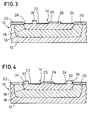
- the NMOS transistor 10 has a weakly p-doped substrate 12, into which an n-well 16 is diffused from the upper side 14. Within this n-well 16 there is a p-well 18 produced by double implantation, which forms the actual substrate region of the NMOS transistor 10. A field oxide layer 20 applied by a LOCOS process is arranged around the p-well 18 on the upper side 14. The n + regions 22, 24 for source and drain as well as the gate oxide layer 26 and the gate electrode 25 located in between are located on the upper side of the substrate 12 within the p-well 18.
- CMOS-LOCOS complementary metal-oxide-semiconductor
- PDEX implantation a two-part implantation achieved after a photolithography step before the poly deposition he follows.
- a depth can be almost any retrograde tub profile with the desired properties Dielectric strength can be set.
- the surface doping, and thus the Threshold voltage of the transistor 10 can be controlled independently by a normal one Threshold voltage implantation can be set.
- the energy of the p-tub implantation is chosen such that the implantation only in the active area, but not through the field oxide layer 20, one achieves one Self-adjustment of the p-tub 18 to the active area edge 34. Together with the small one Diffusion of the implanted p-well 18 allows this in comparison to diffused p-tubs a higher packing density in logic applications.
- the Lateral isolation 23 takes place here by the implantation of the Bird's beak the edges of the active area, the relatively large lateral scatter of the high-energy p-tub implantation and the higher diffusion of the boron implantation compared to the arsenic implantation of the drain and source regions 22, 24.
- the contact 28 of the p-well 18 must be within the same in this case Active area take place (see Fig. 3).
- The serves as the contact implantation Drain / source implantation of those that can be produced using the CMOS process used PMOS transistors. If the p-well potential is below the source potential of the NMOS transistor 10 should be at a sufficient distance 30 between the p + contact 28 and the source or drain region 22, 24 are observed.
- the only process extension is the p-tub implantation (PDEX implantation) however, is used for other manufacturing steps in the LOCOS process does not represent an additional new technology process step.
Landscapes
- Metal-Oxide And Bipolar Metal-Oxide Semiconductor Integrated Circuits (AREA)
- Insulated Gate Type Field-Effect Transistor (AREA)
- Steroid Compounds (AREA)
Abstract
Description
- eine elektrische Isolation des NMOS-Transistors vom Substrat durch zwei pn-Übergänge,
- eine Vermeidung des Substrateffektes durch die Möglichkeit, das Potential der p-Wanne auf das Sourcepotential des Transistors zu legen und
- einen Betrieb der p-Wanne und des Transistors unter Substratpotential.
- Bei einem vorhandenen n-Wannen CMOS-Prozeß ist die Einführung einer zusätzlichen p-Wanne mit kompletter Änderung des Prozeßanfangs (Wannendiffusion/Feldoxidation/Temperaturhaushalt) erforderlich;
- Bei Nutzung von Epi-Substraten ist die Eindringtiefe der n-Wanne durch die Ausdiffusion der Substratdotierung limitiert;
- Bei einer diffundierten p-Wanne ist die Oberflächenkonzentration (Schwellenspannung des NMOS-Transistors) und das Dotierungsprofil in der Tiefe (Isolation/Spannungsfestigkeit des NMOS-Transistors zur n-Wanne) miteinander verkoppelt;
- Eine Anpassung der Wannendotierungen/-diffusionen bedeutet gleichzeitig einen Einfluß auf fast alle anderen Bauelemente.
- die Beibehaltung des bisherigen Wannenkonzeptes (diffundierte n-Wanne) und
- die Erzeugung der p-Wanne durch eine (vorhandene) Implantation,
- wobei keine Änderung des thermischen Haushaltes (Kompatibilität, modulare Prozeßoption) erfolgt.
- Fig. 1
- einen Schnitt durch einen bekannten Well-in-Well NMOS-Transistor, dessen Wannen durch Diffusion erzeugt sind,
- Fig. 2
- einen Schnitt durch einen NMOS-Transistor gemäß einem ersten Ausführungsbeispiel,
- Fig. 3
- einen Schnitt durch einen NMOS-Transistor gemäß einem zweiten Ausführungsbeispiel,
- Fig. 4
- einen Schnitt durch einen NMOS-Transistor gemäß einem dritten Ausführungsbeispiel und
- Fig. 5
- einen quer zu den Schnittansichten der Fign. 2 und 3 verlaufenden Schnitt durch einen NMOS-Transistor gemäß einem vierten Ausführungsbeispiel.
- geringe Oberflächenkonzentration zur Einstellung der Schwellenspannung des NMOS-Transistors 10
- max. Tiefe von ca. 1.5 µm (vorgegeben durch n-Wanne 16)
- Ausreichende Dotierungskonzentration in der Tiefe, um die Isolation des Transistors 10 zur n-Wanne 16 sicherzustellen.
Claims (3)
- NMOS-Transistor miteinem halbleitenden Substrat (12), das p-dotiert ist und eine Oberseite (14) aufweist,einem ersten Gebiet (16), das n-dotiert ist und durch Diffusion von der Oberseite (14) des Substrats (12) in dieses eingebracht ist,einem innerhalb des n-leitenden Gebiets (16) angeordneten zweiten Gebiet (18), das p-dotiert und von der Oberseite (14) des Substrats (12) in dieses eingebracht ist,einer Feldoxidschicht (20), die auf der Oberseite (14) des Substrats (12) angeordnet ist und das p-leitende Gebiet (16) allseitig begrenzt,einem Sourcegebiet (22) sowie einem Draingebiet (24), die n-dotiert sind und voneinander beabstandet innerhalb des p-leitenden Gebiets (18) in der Oberseite (14) des Substrats (12) angeordnet sind,einer Gateoxidschicht (26), die auf der Oberseite (14) des Substrats (12) zwischen dem Source- und dem Draingebiet (22,24) angeordnet ist, undeiner Gateelektrode (25) auf der Gateoxidschicht (26),
dadurch gekennzeichnet,daß das p-leitende Gebiet (18) allseitig durch eine Aktivgebietskante (34) begrenzt ist,daß das p-leitende Gebiet (18) mittels einer Ionenimplantation in das n-leitende Gebiet (16) eingebracht ist, unddaß innerhalb des p-leitenden Gebiets (18) die Ionenkonzentration an der Oberseite (14) des Substrats (12) kleiner ist als an der innerhalb des Substrats (12) angeordneten unteren Grenze des n-leitenden Gebiets (16) zum p-leitenden Gebiet (18). - NMOS-Transistor nach Anspruch 1, dadurch gekennzeichnet, daß das Source- und das Draingebiet (22,24) lateral zum Feldoxid (20) beabstandet (32) sind.
- NMOS-Transistor nach Anspruch 1 oder 2, dadurch gekennzeichnet, daß die Oberseite (14) des Substrats (12) im an das Feldoxid (20) angrenzenden Randbereich des p-leitenden Gebiets (18) zumindest unterhalb einer Gateelektroden-Anschlußbahn (40) mittels p-dotierender Ionenimplantation eine erhöhte Ionenkonzentration zur Unterdrückung eines parasitären NMOS-Transistors (38) aufweist, der von dem Source- oder Draingebiet (22,24), der Gateelektroden-Anschlußbahn (40) und dem n-leitenden Gebiet (16) gebildet ist.
Applications Claiming Priority (4)
| Application Number | Priority Date | Filing Date | Title |
|---|---|---|---|
| DE19828524 | 1998-06-26 | ||
| DE19828524 | 1998-06-26 | ||
| DE19840180 | 1998-09-03 | ||
| DE19840180 | 1998-09-03 |
Publications (3)
| Publication Number | Publication Date |
|---|---|
| EP0967657A2 true EP0967657A2 (de) | 1999-12-29 |
| EP0967657A3 EP0967657A3 (de) | 2007-03-21 |
| EP0967657B1 EP0967657B1 (de) | 2010-01-06 |
Family
ID=26047064
Family Applications (1)
| Application Number | Title | Priority Date | Filing Date |
|---|---|---|---|
| EP99112269A Expired - Lifetime EP0967657B1 (de) | 1998-06-26 | 1999-06-25 | NMOS-Transistor |
Country Status (4)
| Country | Link |
|---|---|
| US (1) | US6137148A (de) |
| EP (1) | EP0967657B1 (de) |
| AT (1) | ATE454716T1 (de) |
| DE (1) | DE59915121D1 (de) |
Families Citing this family (1)
| Publication number | Priority date | Publication date | Assignee | Title |
|---|---|---|---|---|
| DE19940362A1 (de) * | 1999-08-25 | 2001-04-12 | Infineon Technologies Ag | MOS-Transistor und Verfahren zu dessen Herstellung |
Family Cites Families (12)
| Publication number | Priority date | Publication date | Assignee | Title |
|---|---|---|---|---|
| US5324982A (en) * | 1985-09-25 | 1994-06-28 | Hitachi, Ltd. | Semiconductor memory device having bipolar transistor and structure to avoid soft error |
| JPH04239760A (ja) * | 1991-01-22 | 1992-08-27 | Sharp Corp | 半導体装置の製造法 |
| JP2851753B2 (ja) * | 1991-10-22 | 1999-01-27 | 三菱電機株式会社 | 半導体装置およびその製造方法 |
| US5994755A (en) * | 1991-10-30 | 1999-11-30 | Intersil Corporation | Analog-to-digital converter and method of fabrication |
| JPH05198666A (ja) * | 1991-11-20 | 1993-08-06 | Mitsubishi Electric Corp | 半導体装置およびその製造方法 |
| US5376816A (en) * | 1992-06-24 | 1994-12-27 | Nec Corporation | Bi-cmos integrated circuit device having buried region use in common for bipolar and mos transistors |
| US5268312A (en) * | 1992-10-22 | 1993-12-07 | Motorola, Inc. | Method of forming isolated wells in the fabrication of BiCMOS devices |
| JPH07312423A (ja) * | 1994-05-17 | 1995-11-28 | Hitachi Ltd | Mis型半導体装置 |
| US5889315A (en) * | 1994-08-18 | 1999-03-30 | National Semiconductor Corporation | Semiconductor structure having two levels of buried regions |
| US5698458A (en) * | 1994-09-30 | 1997-12-16 | United Microelectronics Corporation | Multiple well device and process of manufacture |
| JP2734436B2 (ja) * | 1995-12-26 | 1998-03-30 | 日本電気株式会社 | Mos型半導体装置 |
| JP2976903B2 (ja) * | 1996-10-08 | 1999-11-10 | 日本電気株式会社 | 半導体記憶装置 |
-
1999
- 1999-06-24 US US09/339,224 patent/US6137148A/en not_active Expired - Lifetime
- 1999-06-25 AT AT99112269T patent/ATE454716T1/de active
- 1999-06-25 DE DE59915121T patent/DE59915121D1/de not_active Expired - Lifetime
- 1999-06-25 EP EP99112269A patent/EP0967657B1/de not_active Expired - Lifetime
Also Published As
| Publication number | Publication date |
|---|---|
| DE59915121D1 (de) | 2010-02-25 |
| US6137148A (en) | 2000-10-24 |
| EP0967657A3 (de) | 2007-03-21 |
| EP0967657B1 (de) | 2010-01-06 |
| ATE454716T1 (de) | 2010-01-15 |
Similar Documents
| Publication | Publication Date | Title |
|---|---|---|
| DE69615458T2 (de) | Dünnfilmtransistor über einem isolierten Halbleitersubstrat und Verfahren zur Herstellung | |
| DE102012100767B4 (de) | Drain-erweiterte Feldeffekttransistoren und Verfahren zu deren Herstellung | |
| DE4233236C2 (de) | Halbleitereinrichtung mit einem Wannenbereich für einen MOS-Transistor und Herstellungsverfahren dafür | |
| DE69728259T2 (de) | Siliciumkarbid-cmos und herstellungsverfahren | |
| DE19642538A1 (de) | Halbleitereinrichtung und Herstellungsverfahren derselben | |
| DE68925116T2 (de) | In gemischter Technologie hergestellte integrierte Schaltung mit CMOS-Strukturen und leistungsfähigen lateralen Bipolartransistoren mit erhöhter Early-Spannung und Herstellungsverfahren dafür | |
| EP0148342B1 (de) | Verfahren zum gleichzeitigen Herstellen von schnellen Kurzkanal- und spannungsfesten MOS-Transistoren in VLSI-Schaltungen | |
| DE2707652A1 (de) | Verfahren zur bildung von kanalsperren entgegengesetzter leitungstypen im zwischenbereich zwischen zwei mos-bauelementen zugeordneten zonen eines siliziumsubstrats | |
| DE3856150T2 (de) | Halbleiteranordnung und verfahren zur herstellung | |
| DE102013022484B3 (de) | Metalloxidhalbleitereinrichtungen | |
| DE69231484T2 (de) | Verfahren zur Herstellung von Isolationszonen des LOCOS-Typs für integrierte Schaltungen vom MOS-Typ | |
| DE19546364A1 (de) | Halbleitervorrichtung und Verfahren zu ihrer Herstellung | |
| DE10256575B4 (de) | Lateraler MOSFET mit hoher Durchbruchspannung und damit ausgestattete Vorrichtung | |
| DE102016202110B4 (de) | Halbleiterstruktur mit Backgate-Gebieten und Verfahren für ihre Herstellung | |
| DE102004009521B4 (de) | Hochvolt-PMOS-Transistor, Maske zur Herstellung einer Wanne und Verfahren zur Herstellung eines Hochvolt-PMOS-Transistors | |
| DE102004018153B4 (de) | Hochvolt-Sperrschicht-Feldeffekttransistor mit retrograder Gatewanne und Verfahren zu dessen Herstellung | |
| DE3686180T2 (de) | Vertikaler mos-transistor mit peripherer schaltung. | |
| EP0853819A1 (de) | Mos-transistor mit hoher ausgangsspannungsfestigkeit | |
| DE19654686C2 (de) | Verfahren zum Herstellen einer Dreiwannen-Anordnung in einer Halbleitervorrichtung | |
| EP2898531B1 (de) | Nmos-transistor und verfahren zu seiner herstellung | |
| DE3932445C2 (de) | Komplementäre Halbleitereinrichtung mit einem verbesserten Isolationsbereich | |
| DE3851419T2 (de) | MOS-Transistor mit erhöhtem Isolationsvermögen. | |
| DE19952742C2 (de) | Halbleiterspeicher-Bauelement, insbesondere ein SRAM, und Verfahren zu seiner Herstellung | |
| EP0088399B1 (de) | Spannungsfester MOS-Transistor für höchstintegrierte Schaltungen | |
| EP0967657B1 (de) | NMOS-Transistor |
Legal Events
| Date | Code | Title | Description |
|---|---|---|---|
| PUAI | Public reference made under article 153(3) epc to a published international application that has entered the european phase |
Free format text: ORIGINAL CODE: 0009012 |
|
| AK | Designated contracting states |
Kind code of ref document: A2 Designated state(s): AT BE CH CY DE DK ES FI FR GB GR IE IT LI LU MC NL PT SE |
|
| AX | Request for extension of the european patent |
Free format text: AL;LT;LV;MK;RO;SI |
|
| PUAL | Search report despatched |
Free format text: ORIGINAL CODE: 0009013 |
|
| AK | Designated contracting states |
Kind code of ref document: A3 Designated state(s): AT BE CH CY DE DK ES FI FR GB GR IE IT LI LU MC NL PT SE |
|
| AX | Request for extension of the european patent |
Extension state: AL LT LV MK RO SI |
|
| 17P | Request for examination filed |
Effective date: 20070804 |
|
| 17Q | First examination report despatched |
Effective date: 20070919 |
|
| AKX | Designation fees paid |
Designated state(s): AT BE CH CY DE DK ES FI FR GB GR IE IT LI LU MC NL PT SE |
|
| GRAP | Despatch of communication of intention to grant a patent |
Free format text: ORIGINAL CODE: EPIDOSNIGR1 |
|
| RIC1 | Information provided on ipc code assigned before grant |
Ipc: H01L 29/78 20060101ALN20090702BHEP Ipc: H01L 29/06 20060101AFI20090702BHEP |
|
| GRAS | Grant fee paid |
Free format text: ORIGINAL CODE: EPIDOSNIGR3 |
|
| GRAA | (expected) grant |
Free format text: ORIGINAL CODE: 0009210 |
|
| AK | Designated contracting states |
Kind code of ref document: B1 Designated state(s): AT BE CH CY DE DK ES FI FR GB GR IE IT LI LU MC NL PT SE |
|
| REG | Reference to a national code |
Ref country code: GB Ref legal event code: FG4D Free format text: NOT ENGLISH |
|
| REG | Reference to a national code |
Ref country code: CH Ref legal event code: EP |
|
| REG | Reference to a national code |
Ref country code: IE Ref legal event code: FG4D |
|
| REF | Corresponds to: |
Ref document number: 59915121 Country of ref document: DE Date of ref document: 20100225 Kind code of ref document: P |
|
| REG | Reference to a national code |
Ref country code: CH Ref legal event code: NV Representative=s name: HEPP WENGER RYFFEL AG |
|
| REG | Reference to a national code |
Ref country code: NL Ref legal event code: T3 |
|
| PG25 | Lapsed in a contracting state [announced via postgrant information from national office to epo] |
Ref country code: PT Free format text: LAPSE BECAUSE OF FAILURE TO SUBMIT A TRANSLATION OF THE DESCRIPTION OR TO PAY THE FEE WITHIN THE PRESCRIBED TIME-LIMIT Effective date: 20100506 Ref country code: ES Free format text: LAPSE BECAUSE OF FAILURE TO SUBMIT A TRANSLATION OF THE DESCRIPTION OR TO PAY THE FEE WITHIN THE PRESCRIBED TIME-LIMIT Effective date: 20100417 |
|
| PG25 | Lapsed in a contracting state [announced via postgrant information from national office to epo] |
Ref country code: FI Free format text: LAPSE BECAUSE OF FAILURE TO SUBMIT A TRANSLATION OF THE DESCRIPTION OR TO PAY THE FEE WITHIN THE PRESCRIBED TIME-LIMIT Effective date: 20100106 |
|
| PG25 | Lapsed in a contracting state [announced via postgrant information from national office to epo] |
Ref country code: SE Free format text: LAPSE BECAUSE OF FAILURE TO SUBMIT A TRANSLATION OF THE DESCRIPTION OR TO PAY THE FEE WITHIN THE PRESCRIBED TIME-LIMIT Effective date: 20100106 Ref country code: GR Free format text: LAPSE BECAUSE OF FAILURE TO SUBMIT A TRANSLATION OF THE DESCRIPTION OR TO PAY THE FEE WITHIN THE PRESCRIBED TIME-LIMIT Effective date: 20100407 Ref country code: CY Free format text: LAPSE BECAUSE OF FAILURE TO SUBMIT A TRANSLATION OF THE DESCRIPTION OR TO PAY THE FEE WITHIN THE PRESCRIBED TIME-LIMIT Effective date: 20100106 |
|
| PLBE | No opposition filed within time limit |
Free format text: ORIGINAL CODE: 0009261 |
|
| 26N | No opposition filed |
Effective date: 20101007 |
|
| PG25 | Lapsed in a contracting state [announced via postgrant information from national office to epo] |
Ref country code: MC Free format text: LAPSE BECAUSE OF NON-PAYMENT OF DUE FEES Effective date: 20100630 Ref country code: DK Free format text: LAPSE BECAUSE OF FAILURE TO SUBMIT A TRANSLATION OF THE DESCRIPTION OR TO PAY THE FEE WITHIN THE PRESCRIBED TIME-LIMIT Effective date: 20100106 |
|
| PGFP | Annual fee paid to national office [announced via postgrant information from national office to epo] |
Ref country code: CH Payment date: 20120622 Year of fee payment: 14 Ref country code: IE Payment date: 20120619 Year of fee payment: 14 Ref country code: NL Payment date: 20120628 Year of fee payment: 14 |
|
| PGFP | Annual fee paid to national office [announced via postgrant information from national office to epo] |
Ref country code: GB Payment date: 20120621 Year of fee payment: 14 |
|
| PG25 | Lapsed in a contracting state [announced via postgrant information from national office to epo] |
Ref country code: LU Free format text: LAPSE BECAUSE OF NON-PAYMENT OF DUE FEES Effective date: 20100625 |
|
| PGFP | Annual fee paid to national office [announced via postgrant information from national office to epo] |
Ref country code: IT Payment date: 20120626 Year of fee payment: 14 |
|
| PGFP | Annual fee paid to national office [announced via postgrant information from national office to epo] |
Ref country code: BE Payment date: 20120622 Year of fee payment: 14 |
|
| PGFP | Annual fee paid to national office [announced via postgrant information from national office to epo] |
Ref country code: AT Payment date: 20120620 Year of fee payment: 14 |
|
| BERE | Be: lapsed |
Owner name: ELMOS SEMICONDUCTOR A.G. Effective date: 20130630 |
|
| REG | Reference to a national code |
Ref country code: NL Ref legal event code: V1 Effective date: 20140101 |
|
| REG | Reference to a national code |
Ref country code: CH Ref legal event code: PL |
|
| REG | Reference to a national code |
Ref country code: AT Ref legal event code: MM01 Ref document number: 454716 Country of ref document: AT Kind code of ref document: T Effective date: 20130625 |
|
| GBPC | Gb: european patent ceased through non-payment of renewal fee |
Effective date: 20130625 |
|
| REG | Reference to a national code |
Ref country code: IE Ref legal event code: MM4A |
|
| PG25 | Lapsed in a contracting state [announced via postgrant information from national office to epo] |
Ref country code: BE Free format text: LAPSE BECAUSE OF NON-PAYMENT OF DUE FEES Effective date: 20130630 |
|
| PG25 | Lapsed in a contracting state [announced via postgrant information from national office to epo] |
Ref country code: GB Free format text: LAPSE BECAUSE OF NON-PAYMENT OF DUE FEES Effective date: 20130625 Ref country code: IE Free format text: LAPSE BECAUSE OF NON-PAYMENT OF DUE FEES Effective date: 20130625 Ref country code: LI Free format text: LAPSE BECAUSE OF NON-PAYMENT OF DUE FEES Effective date: 20130630 Ref country code: CH Free format text: LAPSE BECAUSE OF NON-PAYMENT OF DUE FEES Effective date: 20130630 Ref country code: NL Free format text: LAPSE BECAUSE OF NON-PAYMENT OF DUE FEES Effective date: 20140101 |
|
| PG25 | Lapsed in a contracting state [announced via postgrant information from national office to epo] |
Ref country code: IT Free format text: LAPSE BECAUSE OF NON-PAYMENT OF DUE FEES Effective date: 20130625 Ref country code: AT Free format text: LAPSE BECAUSE OF NON-PAYMENT OF DUE FEES Effective date: 20130625 |
|
| REG | Reference to a national code |
Ref country code: DE Ref legal event code: R082 Ref document number: 59915121 Country of ref document: DE Representative=s name: VON KREISLER SELTING WERNER - PARTNERSCHAFT VO, DE |
|
| REG | Reference to a national code |
Ref country code: DE Ref legal event code: R082 Ref document number: 59915121 Country of ref document: DE Representative=s name: DOMPATENT VON KREISLER SELTING WERNER - PARTNE, DE Effective date: 20150108 Ref country code: DE Ref legal event code: R082 Ref document number: 59915121 Country of ref document: DE Representative=s name: VON KREISLER SELTING WERNER - PARTNERSCHAFT VO, DE Effective date: 20150108 Ref country code: DE Ref legal event code: R081 Ref document number: 59915121 Country of ref document: DE Owner name: ELMOS SEMICONDUCTOR AKTIENGESELLSCHAFT, DE Free format text: FORMER OWNER: ELMOS SEMICONDUCTOR AG, 44227 DORTMUND, DE Effective date: 20150108 |
|
| REG | Reference to a national code |
Ref country code: FR Ref legal event code: PLFP Year of fee payment: 18 |
|
| REG | Reference to a national code |
Ref country code: FR Ref legal event code: PLFP Year of fee payment: 19 |
|
| REG | Reference to a national code |
Ref country code: FR Ref legal event code: PLFP Year of fee payment: 20 |
|
| PGFP | Annual fee paid to national office [announced via postgrant information from national office to epo] |
Ref country code: DE Payment date: 20180625 Year of fee payment: 20 |
|
| PGFP | Annual fee paid to national office [announced via postgrant information from national office to epo] |
Ref country code: FR Payment date: 20180625 Year of fee payment: 20 |
|
| REG | Reference to a national code |
Ref country code: DE Ref legal event code: R071 Ref document number: 59915121 Country of ref document: DE |