EP0959325A2 - Commutateur photo-électrique, commutateur photo-électrique à fibre optique et détecteur distinguant les couleurs - Google Patents
Commutateur photo-électrique, commutateur photo-électrique à fibre optique et détecteur distinguant les couleurs Download PDFInfo
- Publication number
- EP0959325A2 EP0959325A2 EP99108637A EP99108637A EP0959325A2 EP 0959325 A2 EP0959325 A2 EP 0959325A2 EP 99108637 A EP99108637 A EP 99108637A EP 99108637 A EP99108637 A EP 99108637A EP 0959325 A2 EP0959325 A2 EP 0959325A2
- Authority
- EP
- European Patent Office
- Prior art keywords
- light
- optical
- light emission
- lens
- optical axis
- Prior art date
- Legal status (The legal status is an assumption and is not a legal conclusion. Google has not performed a legal analysis and makes no representation as to the accuracy of the status listed.)
- Granted
Links
Images


Classifications
-
- G—PHYSICS
- G02—OPTICS
- G02B—OPTICAL ELEMENTS, SYSTEMS OR APPARATUS
- G02B26/00—Optical devices or arrangements for the control of light using movable or deformable optical elements
- G02B26/08—Optical devices or arrangements for the control of light using movable or deformable optical elements for controlling the direction of light
-
- G—PHYSICS
- G02—OPTICS
- G02B—OPTICAL ELEMENTS, SYSTEMS OR APPARATUS
- G02B6/00—Light guides; Structural details of arrangements comprising light guides and other optical elements, e.g. couplings
- G02B6/24—Coupling light guides
- G02B6/42—Coupling light guides with opto-electronic elements
- G02B6/4201—Packages, e.g. shape, construction, internal or external details
- G02B6/4204—Packages, e.g. shape, construction, internal or external details the coupling comprising intermediate optical elements, e.g. lenses, holograms
- G02B6/4215—Packages, e.g. shape, construction, internal or external details the coupling comprising intermediate optical elements, e.g. lenses, holograms the intermediate optical elements being wavelength selective optical elements, e.g. variable wavelength optical modules or wavelength lockers
-
- G—PHYSICS
- G01—MEASURING; TESTING
- G01V—GEOPHYSICS; GRAVITATIONAL MEASUREMENTS; DETECTING MASSES OR OBJECTS; TAGS
- G01V8/00—Prospecting or detecting by optical means
- G01V8/10—Detecting, e.g. by using light barriers
- G01V8/12—Detecting, e.g. by using light barriers using one transmitter and one receiver
- G01V8/16—Detecting, e.g. by using light barriers using one transmitter and one receiver using optical fibres
-
- G—PHYSICS
- G02—OPTICS
- G02B—OPTICAL ELEMENTS, SYSTEMS OR APPARATUS
- G02B6/00—Light guides; Structural details of arrangements comprising light guides and other optical elements, e.g. couplings
- G02B6/24—Coupling light guides
- G02B6/42—Coupling light guides with opto-electronic elements
- G02B6/4298—Coupling light guides with opto-electronic elements coupling with non-coherent light sources and/or radiation detectors, e.g. lamps, incandescent bulbs, scintillation chambers
-
- G—PHYSICS
- G02—OPTICS
- G02B—OPTICAL ELEMENTS, SYSTEMS OR APPARATUS
- G02B6/00—Light guides; Structural details of arrangements comprising light guides and other optical elements, e.g. couplings
- G02B6/24—Coupling light guides
- G02B6/26—Optical coupling means
- G02B6/28—Optical coupling means having data bus means, i.e. plural waveguides interconnected and providing an inherently bidirectional system by mixing and splitting signals
- G02B6/293—Optical coupling means having data bus means, i.e. plural waveguides interconnected and providing an inherently bidirectional system by mixing and splitting signals with wavelength selective means
- G02B6/29346—Optical coupling means having data bus means, i.e. plural waveguides interconnected and providing an inherently bidirectional system by mixing and splitting signals with wavelength selective means operating by wave or beam interference
- G02B6/29361—Interference filters, e.g. multilayer coatings, thin film filters, dichroic splitters or mirrors based on multilayers, WDM filters
- G02B6/29362—Serial cascade of filters or filtering operations, e.g. for a large number of channels
Definitions
- This invention relates to an optical unit, a photoelectric switch, and a fiber-type photoelectric switch each comprising a plurality of optical elements, and a color discrimination sensor for detecting color of an object.
- an optical unit such as a photoelectric switch has been used for emitting light to an object and receiving the light reflected on the object or the light penetrating the object, thereby detecting information on the object.
- the photoelectric switch With the photoelectric switch, light is emitted to a transport passage of an object and the presence or absence, the shape, the dimensions, the color, etc., of the object can be detected on the basis or the light reception quantity of the reflected light or penetrating light.
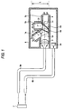
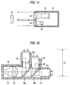
- FIG. 11 is a sectional view to show an example of a photoelectric switch in a related art.
- a light emission element 31 and a light reception element 32 are placed in a housing 35.
- Light emitted from the light emission element 31 is transmitted through a projection lens 33 to a detection position.
- Light from the detection position is gathered through a light reception lens 34 at the light reception element 32. If an object 37 exists at the detection position, light reflected from the object 37 is received on the light reception element 32 through the light reception lens 34. Therefore, whether or not the object 37 exists can be determined on the basis of the light reception quantity level of the light reception element 32.
- a color discrimination sensor which is also a kind of photoelectric switch, comprises a light transmission section containing a light source consisting of three light emission elements for respectively generating lights having wavelength bands corresponding to Red, Green and Blue and a projection lens for transmitting light emitted from each light emission element to an object and a light reception section having a detection light reception element for receiving light reflected from the object.
- each of the three light emission elements Light emitted from each of the three light emission elements is transmitted through the projection lens to the object in order and reflected light is received on the detection light reception element, then the color of the object can be determined on the basis of the light reception quantity level off each color band, for example, from comparison with reference color.
- FIG. 12 is a sectional, view of the main part of an optical unit having a plurality of light emission elements in a related art.
- three light emission elements 41a, 41b, and 41c, a projection lens 42, and two dichroic mirrors 43a and 43b are disposed in a holder 40.
- the light emission element 41c is placed so that an optical axis LC of the light emission element 41c matches an optical axis LX of the projection lens 42.
- the light emission element 41b is placed so that an optical axis LB of the light emission element 41b crosses the optical axis LX of the projection lens 42 at right angles.
- the light emission element 41a is placed so that an optical axis LA of the light emission element 41a crosses the optical axis LX of the projection lens 42 at right angles.
- the light emission element 41a If the light emission element 41a is turned on, light emitted from the light emission element 41a is reflected on the dichroic mirror 43a and is transmitted through the projection lens 42. If the light emission element 41b is turned on, light emitted from the light emission element 41b is reflected on the dichroic mirror 43b and the reflected light penetrates the dichroic mirror 43a and is transmitted through the projection lens 42. If the light emission element 41c is turned on, light emitted from the light emission element 41c penetrates the dichroic mirrors 43b and 43a and is transmitted through the projection lens 42.
- the total of the optical path length from the light emission element 41a to the dichroic mirror 43a and the optical path length from the dichroic mirror 43a to the projection lens 42, the total of the optical path length from the light emission element 41b to the dichroic mirror 43b and the optical path length from the dichroic mirror 43b to the projection lens 42, and the optical path length from the light emission element 41c to the projection lens 42 are set almost equal to each other considering the light wavelength.
- the distance from the light emission element 41a at a position near the projection lens 42 to the optical axis LX of the projection lens 42 becomes long as compared with the distance from the light emission element 41b at a position distant from the projection lens 42 to the optical axis LX of the projection lens 42. Resultantly, the width of the optical unit, LO, increases and it is difficult to miniaturize the unit.
- an optical unit for emitting or receiving light comprising a plurality of optical elements for emitting or receiving light, a lens for transmitting or receiving light, and an optical system for guiding light from the optical elements into the lens or guiding light from the lens into the optical elements, wherein the optical elements and the lens are placed so that an optical axis of at least one of the optical elements crosses an optical axis of the lens with an inclination thereto.
- the optical system guides light emitted from the optical elements into the lens or guides light from the lens into the optical elements.
- the optical elements and the lens are placed so that the optical axis of at least one of the optical elements crosses the optical axis of the lens with an inclination thereto, whereby the distance between the optical element and the optical axis of the lens is shortened. Therefore, the optical unit can be miniaturized while the optical path lengths from the optical elements to the lens are held equal to each other.
- the optical axes of the optical elements are preferably placed in three dimensions.
- the optical unit can be miniaturized in the width and thickness directions.
- the optical element of the optical elements positioned nearest to the lens is a light emission element for emitting green band light.
- the attenuation effect of the optical system on the light emission element for emitting green band light with the smallest light reception detection output as compared with the light emission element for emitting blue or red band light can be decreased.
- a photoelectric switch for transmitting light to a detection position and receiving light reflected from the detection position or tight penetrating the detection position
- the photoelectric switch comprising a plurality of light emission elements for emitting light, a projection lens for transmitting light from the light emission elements to the detection position in order, an optical system for guiding light emitted from the light emission elements into the projection lens, and a light reception element for receiving light reflected from the detection position or light penetrating the detection position, wherein the light emission elements and the projection lens are placed so that an optical axis of at least one of the light emission elements crosses an optical axis of the projection lens with an inclination thereto.
- the light emission elements and the projection lens are placed so that the optical axis of at least one of the light emission elements crosses the optical axis of the projection lens with an inclination thereto, whereby the distance from the light emission element to the optical axis of the projection lens is shortened and the photoelectric switch can be miniaturized.
- the light emission elements are preferably placed in the ascending order of light reception element output values corresponding to light emitted from the optical elements to the projection lens.
- the optical element which provides smaller light reception detection output can decrease the attenuation effect of the optical system more largely.
- a fiber type photoelectric switch for transmitting light to a detection position and receiving light reflected from the detection position or light penetrating the detection position
- the fiber type photoelectric switch comprising a plurality of light emission elements for emitting light, a projection lens for transmitting light emitted from the light emission elements, a first optical fiber for guiding the light emitted from the light emission elements and penetrating the projection lens into the detection position, a detection light reception element, and a second optical fiber for guiding the light reflected from the detection position or the light penetrating the detection position into the detection light reception element, wherein the light emission elements and the projection lens are placed so that an optical axis of at least one of the light emission elements crosses an optical axis of the projection lens with an inclination thereto.
- the light emission elements and the projection lens are placed so that the optical axis of at least one of the light emission elements crosses the optical axis of the projection lens with an inclination thereto, whereby the distance between the light emission element and the optical axis of the projection lens is shortened and the fiber type photoelectric switch can be miniaturized.
- the optical elements are placed in the ascending order of light reception element output values corresponding to light emitted from the optical elements to the projection lens.
- the optical element which provides smaller light reception detection output can decrease the attenuation effect of the optical system more largely.
- a color discrimination sensor for transmitting light to an object and detecting color (that is, wavelength band) of the object based on light reflected from the object
- the color discrimination sensor comprising a first light emission element, a second light emission element, and a third light emission element for emitting light in different wavelength bands, a projection lens for transmitting light emitted from the first, second, and third light emission elements to the object, an optical system for guiding light emitted from the first, second, and third light emission elements into the projection lens, and a detection light reception element for receiving the light reflected from the object
- the first light emission element is disposed on an optical axis of the projection lens so that an optical axis of the first light emission element matches the optical axis of the projection lens
- the second light emission element is placed at a position distant from the optical axis of the projection lens to the side of the projection lens from the first light emission element so that an optical axis of the second light emission element crosses the optical axis of
- the distance between the third light emission element and the optical axis of the projection lens can be shortened and the color discrimination sensor can be miniaturized.
- the light emission elements are placed as the third light emission element, the second light emission element, and the first light emission element in the ascending order of light reception element output values corresponding to light emitted from the tight emission elements to the projection lens.
- the optical element which provides smaller light reception detection output can decrease the attenuation effect of the optical system more largely.
- an optical unit comprising a first optical element, a second optical element, and a third optical element for emitting or receiving light, a lens for transmitting or receiving light, and an optical system for guiding light from the optical elements into the lens or guiding light from the lens into the optical elements, wherein the first optical element is disposed on an optical axis of the lens so that an optical axis of the first optical element matches the optical axis of the lens, the second optical element is placed at a position distant from the optical axis of the lens to the side of the lens from the first optical element so that an optical axis of the second optical element crosses the optical axis of the lens at right angles, and the third optical element is placed at a position distant from the optical axis of the lens to the side of the lens from the second optical element so that an optical axis of the third optical element crosses the optical axis of the lens with an inclination thereto at an acute angle.
- the third optical element is placed so that the optical axis of the third optical element crosses the optical axis of the lens with an inclination thereto at an acute angle, so that the distance between the third light emission element and the optical axis of the lens is shortened and the optical unit can be miniaturized.
- the third optical element is a light emission element for emitting green band light.
- the attenuation effect of the optical system on the light emission element for emitting green band light with the smallest light reception detection output as compared with the light emission element for emitting blue or red band light can be decreased.
- an optical unit comprising a first optical element, a second optical element, and a third optical element for emitting or receiving light, a lens for transmitting or receiving light, and an optical system for guiding light from the optical elements into the lens or guiding light from the lens into the optical elements, wherein the first optical element is disposed on an optical axis of the lens so that an optical axis of the first optical element matches the optical axis of the lens, the second optical element is placed at a position distant from the optical axis of the lens to the side of the lens from the first optical element so that an optical axis of the second optical element crosses the optical axis of the lens with an inclination thereto at an acute angle, and the third optical element is placed at a position distant from the optical axis of the lens on a plane different from the second optical element so that an optical axis of the third optical element crosses the optical axis of the lens with an inclination thereto at an acute angle.
- the cross angle is adjusted three-dimensionally and as at an acute angle and the optical elements are placed so that the distances from the optical axis of the lens to the second and third optical elements are shortened, thus the optical unit can be miniaturized.
- the third optical element is a light emission element for emitting green band light.
- the attenuation effect of the optical system on the light emission element for emitting green band light with the smallest light reception detection output as compared with the light emission element for emitting blue or red band light can be decreased.
- an optical unit for emitting light comprising a blue light emission element, a green light emission element, a red light emission element, a projection lens for transmitting light from the light emission elements, a first dichroic mirror capable of reflecting light of light emission wavelength of the green light emission element and allowing light of light emission wavelengths of the blue and red light emission elements to pass through, and a second dichroic mirror capable of reflecting light of light emission wavelength of one of the blue and red light emission elements and allowing light of light emission wavelengths of the other to pass through, wherein optical path lengths from the light emission elements to the projection lens equal and the green light emission element is disposed nearest to the projection lens among the light emission elements.
- the light reception detection output of each color is adjusted for suppressing variations.
- the optical element with the lowest light reception detection output among the optical elements is disposed at an optical position with the minimum attenuation effect as compared with others, namely, at a position near the projection lens, whereby bottom up of ability of the entire optical unit is enabled.
- FIG. 1 is a sectional view of the main part of a fiber type photoelectric switch according to the first embodiment of the invention.
- the photoelectric switch shown in FIG. 1 can also be used as a color discrimination sensor. It comprises a housing 8, a holder 9 placed in the housing 8, three light emission elements 1a, 1b, and 1c, a projection lens 3, and two dichroic mirrors 5a and 5b disposed in the holder 9, a detection light reception element 2a below the holder 9, and a pair of optical fibers 6a and 6b attached to the front of the housing 8.
- the light emission elements 1a, 1b, and 1c are, for example, light emitting diodes and emit light of different wavelength bands.
- the light emission element 1a emits green light (that is, a light having a range of wavelength corresponding to green)
- the light emission element 1b emits blue light (that is, a light having a range of wavelength corresponding to blue)
- the light emission element 1c emits red light (that is, a light having a range of wavelength corresponding to red).
- the light emission element 1c is placed so that an optical axis Lc of the light emission element 1c matches an optical axis Lx of the projection lens 3.
- the light emission element 1b is placed so that an optical axis Lb of the light emission element 1b crosses the optical axis Lx of the projection lens 3 at right angles.
- the light emission element 1a is placed so that an optical axis La of the light emission element 1a crosses the optical axis Lx of the projection lens 3 at an angle of greater than 0 degrees and smaller than 90 degrees.
- Each of the dichroic mirrors 5a and 5b reflects light of a specific wavelength band and allows light of any other wavelength to pass through.
- the dichroic mirror 5a reflects light of the light emission wavelength of the light emission element 1a and allows light of any other wavelength to pass through.
- the dichroic mirror 5b reflects light of the light emission wavelength of the light emission element 1b and allows light of any other wavelength to pass through.
- the dichroic mirror 5b is placed so as to allow light emitted from the light emission element 1c to pass through and guide the light into the projection lens 3 and reflect light emitted from the light emission element 1b and guide the light into the projection lens 3.
- the dichroic mirror 5a is placed so as to allow light penetrating the dichroic mirror 5b from the light emission element 1c and light reflected on the dichroic mirror 5b from the light emission element 1b to pass through and guide the light into the projection lens 3 and reflect light emitted from the light emission element 1a and guide the light into the projection lens 3.
- the light emission elements 1a, 1b, and 1c, the projection lens 3, and the dichroic mirrors 5a and 5b are placed so that the total of the optical path length from the light emission element 1a to the dichroic mirror 5a and the optical path length from the dichroic mirror 5a to the projection lens 3, the total of the optical path length from the light emission element 1b to the dichroic mirror 5b and the optical path length from the dichroic mirror 5b to the projection lens 3, and the optical path length from the light emission element 1c to the projection lens 3 substantially match.
- the projection lens 3 is placed so as to gather light from the light emission elements 1a, 1b, and 1c at one end of the optical fiber 6a.
- the detection light reception element 2a is made of a photodiode, for example. It is placed so as to face one end of the optical fiber 6b.
- the placement order of the light emission elements 1a, 1b, and 1c is determined by the tight emission power of the light emission elements and the spectral sensitivity of a photodiode used as the light reception element 2a, as parameters. The determination method of the placement order will be discussed.
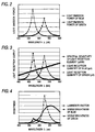
- the light emission power of the light emission element 1 generally has a distribution characteristic responsive to the wavelength as shown in FIG. 2 which shows the relationship between the wavelength and light emission power, and luminescent color can be recognized visually from the wavelength distribution of the light emission power.
- FIG. 2 shows the relationship between the wavelength and light emission power
- luminescent color can be recognized visually from the wavelength distribution of the light emission power.
- FIG. 2 shows the relationship between the wavelength and light emission power
- light emitted from the blue light emission element (with the light emission power having the peak 470 nm and distributed in the range of 400 nm to 550 nm) can be recognized as blue and light emitted from the green light emission element (with the light emission power having the peak 525 nm and distributed in the range of 450 nm to 600 nm) can be recognized as green.
- the light emission power of the red light emission element is not shown, it has a peak at a point near 700 nm.
- a photodiode or a phototransistor is used as the light reception element 2a; it changes in sensitivity depending on the wavelength of incident light.
- the silicon family photodiode or phototransistor has the highest sensitivity in the range of 800 run to 1000 nm in the infrared area, namely, unvisual wavelength band; the sensitivity lowers in any other wavelength range.
- FIG. 3 shows an example of the spectral sensitivity of the light reception element rising toward 800 nm from left to right.
- the level of a detection signal that can be taken out as light reception element output is determined by the relationship between the wavelength distribution of the light emission power of the light emission elements 1 and the spectral sensitivity difference depending on the wavelength of the light reception element 2a.
- the light reception element output corresponding to one color light emission element differs from the light reception element output corresponding to another and there is the light emission element causing the signal level of the light reception element output to reach the minimum.
- the signal levels can be compared, for example, as follows:
- the spectral sensitivity for each wavelength of the light reception element 2a is represented as p ( ⁇ )
- the first column of the table indicates the wavelengths of light in 5-nm steps of 400 nm to 650 nm.
- the second column indicates the light emission power B of the blue LED
- the third column indicates the light emission power G of the green LED
- the fourth column indicates the spectral sensitivity PD of the light reception element
- the fifth column indicates light reception element output when the blue LED emits light B*PD (product of light emission power B of the blue LED and spectral sensitivity PD)
- the sixth indicates light reception element output when the green LED emits light G*PD (product of light emission power G of the green LED and spectral sensitivity PD).
- FIG. 2 is provided by plotting the numeric values under the second and third columns of the above-mentioned Table.
- FIG. 3 is provided by plotting the numeric values of the spectral sensitivity of the light reception element under the fourth column of the above-mentioned Table, the numeric values of output of the light reception element indicated under the fifth column (product of light emission power of the blue LED and spectral sensitivity of the light reception element), and the numeric values of output of the light reception element indicated under the sixth column (product of light emission power of the green LED and spectral sensitivity of the light reception element).
- the sum total (possibly, representing the integral value) of the light reception element output of the green LED is smaller than that of the blue LED. Therefore, it is understood that the integral value of the light reception element output corresponding to the blue LED is greater than that corresponding to the green LED and that the level of the light reception element output corresponding to the blue LED becomes higher.
- a comparison with the level of the light reception element output corresponding to the red LED can also be made by a similar method.
- the level of the light reception element output corresponding to the red LED will not be discussed in detail, because it is clear that the level of the light reception element output corresponding to the red LED becomes larger than that corresponding to the blue or green LED as generally a light reception element of a silicon-family photodiode, phototransistor, etc., has a spectral sensitivity rising from left to right with a peak in the area of 800 nm or more and the red LED has the light emission output peak near 700 nm.
- FIG. 4 is provided by plotting the numeric values listed under the seventh to ninth columns of the Table.
- the brightness of the light emission element of each color according to the luminosity factor observed with human being eyes can be found by the product of the light emission power of each LED and luminosity factor.
- the sum total of the brightness of the green LED in the wavelength range of 400 nm to 650 nm in 5-nm steps is larger than that of the brightness of the blue LED. Therefore, the visible brightness of the light emission output of the blue LED becomes considerably smaller than that of the green LED.
- a comparison with the visible brightness of the light emission output of the red LED can also be made by a similar method.
- the visible brightness of the light emission output of the green LED becomes a higher level than that of the blue LED, but the actual light reception output of the light reception element corresponding to the green LED becomes smaller than that corresponding to the blue LED.
- the inventor considers the placement order of the light emission elements of the whole optical unit based on the knowledge. That is, the optical system is designed by assigning the highest priority to the light emission element which becomes the lowest level when the light reception outputs corresponding to the light sources of the wavelengths, namely, the output signal levels of the light reception element are compared. In other words, light is emitted from each light source and is received at the light reception element under the same condition and the light source having the smallest output signal level is assigned the highest priority for designing the optical system.
- the green LED 1a whose light reception element output level is the lowest is disposed optically and physically nearest to the projection lens 3
- the blue LED 1b whose light reception element output level is the second lowest is disposed next to the green LED 1a
- the red LED 1c whose light reception element output level is the highest is disposed most distant from the projection lens 3.
- the reason why the LEDs are thus placed is that while light from the red LED 1c arrives at the projection lens 3, it is attenuated twice as it penetrates the dichroic mirror 5b and the dichroic mirror 5a and that while light from the blue LED 1b arrives at the projection lens 3, it is attenuated twice as it is reflected on the dichroic mirror 5b and penetrates the dichroic mirror 5a, but while light from the green LED 1a arrives at the projection lens 3, it is attenuated only once as it is only reflected on the dichroic mirror 5a.
- the calculation value data varies with the elements and drive conditions and is not constant.
- the order of red, green, and blue changes depending on the characteristics of the elements. Although blue B and green G have been examined, red R can also be examined likewise.
- light emitted from the Light emission element causing the output at the light reception element to reach the minimum level is made to skip penetration of the dichroic mirrors 5a and 5b for lessening the attenuation degree of the output, so that the incident light quantity on the light reception element can be raised relatively for adjusting the level of the corresponding color light reception element output.
- the optical fiber 6a transmits light gathered at one end through the projection lens 3 to the other end and guides the light into a detection position 7 and the optical fiber 6b transmits light reflected from the detection position 7 and incident on one end to the other end and guides the light into the detection light reception element 2a, whereby if the distance from the photoelectric switch to the detection position 7 is longer than the tolerance that can be detected in the configuration using the LEDs, the optical fibers 6a and 6b enable light transmission and detection.
- the light emission elements 1a, 1b, and 1c are turned on in order in a time division way. If the light emission element 1a is turned on, green light emitted from the light emission element 1a is reflected on the dichroic mirror 5a and is guided through the projection lens 3 and the optical fiber 6a into the detection position. If the light emission element 1b is turned on, blue light emitted from the light emission element 1b is reflected on the dichroic mirror 5b, penetrates the dichroic mirror 5a, and is guided through the projection lens 3 and the optical fiber 6a into the detection position.
- red light emitted from the light emission element 1c penetrates the dichroic mirrors 5b and 5a and is guided through the projection lens 3 and the optical fiber 6a into the detection position. If an object 7 exists at the detection position, reflected light from the object 7 is guided through the optical fiber 6b into the detection light reception element 2a. Color of the object 7 can be detected according to color detection based on the color light reception quantities of green, blue, and red, light reception quantity percentage of R, G, and B, etc., in addition to shape and position detection of the object (workpiece) 7 based on reflected light and penetrating light received at the detection light reception element 2a.
- Change can also be made whenever necessary so that the object (workpiece) 7 can be detected according to penetrating light received at the detection light reception element 2a by placing the optical fiber 2b on the light reception side in FIG. 1 on the opposite side to the object 7.
- FIG. 5 is a block diagram of a control system of the photoelectric switch shown in FIG. 1.
- a control section 20 gives light emission timing control signals Ta, Tb, and Tc for controlling the light emission timings of the light emission elements 1a, 1b, and 1c to drive sections 21a, 21b, and 21c respectively.
- the drive sections 21a, 21b, and 21c respond to the light emission timing control signals Ta, Tb, and Tc with driving of the light emission elements 1a, 1b, and 1c respectively.
- An output signal of the detection light reception element 2a is amplified by an amplifier 22a and is given to the control section 20 as a light reception signal RS.
- the control section 20 outputs a detection signal DE based on the level of the light reception signal RS. For example, if the level of the light reception signal RS is higher than a predetermined threshold value, the control section 20 outputs the detection signal DE high; if the level of the light reception signal RS is lower than the predetermined threshold value, the control section 20 outputs the detection signal DE low.
- the light emission element 1a and the projection lens 3 are placed so that the optical axis La of the light emission element 1a near to the projection lens 3 crosses the optical axis LX of the projection lens 3 with an inclination thereto, so that the width of the holder 9 of the photoelectric switch, L, can be lessened while the optical path lengths from the light emission elements 1a, 1b, and 1c to the projection lens 3 are held equal to each other.
- FIG. 6 is a sectional view of the main part of a photoelectric switch according to the second embodiment of the invention.
- the photoelectric switch shown in FIG. 7 differs from the photoelectric switch in FIG. 1 in that it does not comprise optical fibers and is provided with a light reception lens 4.
- a projection lens 3 transmits light from light emission elements 1a, 1b, and 1c to a detection position.
- the light reception lens 4 gathers light from the detection position at a detection light reception element 2a. If an object 7 exists at the detection position, reflected light from the object 7 is gathered through the light reception lens 4 at the detection light reception element 2a.
- the configuration of a control system of the photoelectric switch shown in FIG. 6 may be the same as the configuration shown in FIG. 5.
- the light emission element 1a and the projection lens 3 are placed so that an optical axis La of the light emission element 1a near to the projection lens 3 crosses an optical axis LX of the projection lens 3 with an inclination thereto, so that the width of the holder 9 of the photoelectric switch, L, can be lessened while the optical path lengths from the light emission elements 1a, 1b, and 1c to the projection lens 3 are held equal to each other.
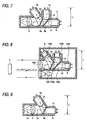
- FIG. 7 is a sectional view of the main part of an optical unit according to the third embodiment of the invention.
- FIG. 7 in an optical unit utilized as a light transmission unit, three light emission elements 1a, 1b, and 1c, a projection lens 3, and two dichroic mirrors 5a and 5b are disposed in a holder 9.
- the light emission elements 1a, 1b, and 1c, the dichroic mirrors 5a and 5b, and the projection lens 3 are placed as those of the photoelectric switch in FIG. 1.
- the light emission element 1a and the projection lens 3 are placed so that an optical axis La of the light emission element 1a near to the projection lens 3 crosses an optical axis LX of the projection lens 3 with an inclination thereto, so that the width of the optical unit, L, can be lessened while the optical path lengths from the light emission elements 1a, 1b, and 1c to the projection lens 3 are held equal to each other.
- FIG. 7 has been described as a light transmission unit, but the light emission elements 1a, 1b, and 1c can be all replaced with light reception elements, for example, to form a light reception unit.
- FIG. 8 shows a modified example of the optical unit for transmitting light of a white light 100 (for example, a halogen lamp) to an object 7 and receiving light reflected on the object 7 or light penetrating the object 7, thereby detecting information on the object 7.
- Green light G passing through a lens 103 is reflected on a dichroic mirror 105a and is received at a green light reception element 102a.
- Blue light B passing through the lens 103 passes through the dichroic mirror 105a, is reflected on a dichroic mirror 105b, and is received at a blue light reception element 102b.
- Red light R passing through the lens 103 passes through the dichroic mirrors 105a and 105b and is received at a red light reception element 102c.
- FIG. 9 is a sectional view of the main part of an optical unit according to the fourth embodiment of the invention.
- the embodiment is a configuration example comprising two optical elements (light emission or reception elements).
- two light emission elements 1a and 1c, a projection lens 3, and a dichroic mirror 5a is placed in a holder 9.
- the light emission element 1c is placed so that an optical axis LC of the light emission element 1c matches an optical axis LX of the projection lens 3.
- the light emission element 1a is placed so that an optical axis La of the light emission element 1a crosses the optical axis LX of the projection lens 3 at an angle of greater than 0 degrees and smaller than 90 degrees (acute angle).
- the total of the optical path length from the light emission element 1a to the dichroic mirror 5a and the optical path length from the dichroic mirror 5a to the projection lens 3 and the optical path length from the light emission element 1c to the projection lens 3 is set equal to each other.
- the light emission element 1a and the projection lens 3 are placed so that the optical axis La of the light emission element 1a near to the projection lens 3 crosses the optical axis LX of the projection lens 3 with an inclination thereto, so that the width of the optical unit, L, can be lessened while the optical path lengths from the light emission elements 1a and 1c to the projection lens 3 are held equal to each other.
- a light reception element or elements may replace either or both of the light emission elements 1a and 1c.
- a light reception element is provided in place of the light emission element 1a and a half mirror is used in place of the dichroic mirror 5a, whereby a small photoelectric switch comprising a light emission element 1c and a light reception element 1a can be formed.
- the embodiment is a configuration example comprising optical elements placed in three dimensions.
- FIGS. 10A and 10B are a front view and a plan view of the main part of an optical unit according to the fifth embodiment of the invention.
- a light emission element 1c is placed so that an optical axis Lc of the light emission element 1c matches an optical axis LX of a projection lens 3.
- a light emission element 1b is placed so that an optical axis Lb of the light emission element 1b crosses the optical axis LX of the projection lens 3 at an angle of greater than 0 degrees and smaller than 90 degrees (acute angle).
- a light emission element 1a is placed so that an optical axis La of the light emission element 1a crosses the optical axis LX of the projection lens 3 at an angle of greater than 0 degrees and smaller than 90 degrees (acute angle). Further, the optical axis Lb of the light emission element 1b is on a vertical plane and the optical axis La of the light emission element 1a is on a horizontal plane.
- the total of the optical path length from the light emission element 1a to the dichroic mirror 5a and the optical path length from the dichroic mirror 5a to the projection lens 3, the total of the optical path length from the light emission element 1b to the dichroic mirror 5b and the optical path length from the dichroic mirror 5b to the projection lens 3, and the optical path length from the light emission element 1c to the projection lens 3 are set equal to each other.
- a light reception element or elements can replace any or all of the light emission elements 1a, 1b, and 1c.
- the optical axis La of the light emission element 1a and the optical axis Lb of the light emission element 1b cross the optical axis LX of the projection lens 3 with an inclination thereto, and are placed on different planes, in which case the dimensions of the optical unit can be shortened in two directions of the width and thickness.
- dichroic mirrors are used as the optical members of the optical system, other members of half mirrors, optical waveguides, etc., may be used as the optical members.
- the projection lens comprises one lens, but may be formed of more than one lens.
- the optical members are placed so that the optical axis of at least one optical element crosses the optical axis of the lens with an inclination thereto, so that the unit can be miniaturized while the optical path lengths from the optical elements to the lens are held equal to each other.
- the optical element with the lowest light reception detection output among the optical elements different in wavelength band is disposed at an optical position with the minimum attenuation effect, namely, at a position near the lens, whereby the light reception detection output of each color is adjusted for suppressing variations, so that the optical unit improved in product level can be provided.
- the present invention is based on Japanese Patent Application No. Hei 10-138941, which is incorporated herein by reference.
Applications Claiming Priority (2)
| Application Number | Priority Date | Filing Date | Title |
|---|---|---|---|
| JP13894198 | 1998-05-20 | ||
| JP13894198A JP4033550B2 (ja) | 1998-05-20 | 1998-05-20 | 光学装置、光電スイッチ、ファイバ型光電スイッチおよび色識別センサ |
Publications (3)
| Publication Number | Publication Date |
|---|---|
| EP0959325A2 true EP0959325A2 (fr) | 1999-11-24 |
| EP0959325A3 EP0959325A3 (fr) | 2001-01-24 |
| EP0959325B1 EP0959325B1 (fr) | 2008-07-23 |
Family
ID=15233739
Family Applications (1)
| Application Number | Title | Priority Date | Filing Date |
|---|---|---|---|
| EP99108637A Expired - Lifetime EP0959325B1 (fr) | 1998-05-20 | 1999-05-12 | Détecteur distinguant les couleurs |
Country Status (6)
| Country | Link |
|---|---|
| US (1) | US6323481B2 (fr) |
| EP (1) | EP0959325B1 (fr) |
| JP (1) | JP4033550B2 (fr) |
| KR (1) | KR100567997B1 (fr) |
| DE (1) | DE69939141D1 (fr) |
| TW (1) | TW439357B (fr) |
Families Citing this family (16)
| Publication number | Priority date | Publication date | Assignee | Title |
|---|---|---|---|---|
| US6776109B2 (en) | 2000-12-13 | 2004-08-17 | Columbia Insurance Company | Bow and skew control system and method |
| JP4266180B2 (ja) | 2003-10-07 | 2009-05-20 | 株式会社キーエンス | 光電センサ |
| US7502112B2 (en) * | 2004-12-23 | 2009-03-10 | Brytech Inc. | Colorimetric device and colour determination process |
| EP2278361B2 (fr) * | 2009-07-23 | 2022-02-23 | Sick Ag | Capteur optoélectronique |
| JP5349185B2 (ja) * | 2009-07-24 | 2013-11-20 | 株式会社キーエンス | 光電センサ及び光電センサシステム |
| US8665442B2 (en) | 2011-08-18 | 2014-03-04 | Li-Cor, Inc. | Cavity enhanced laser based isotopic gas analyzer |
| JP2013178129A (ja) * | 2012-02-28 | 2013-09-09 | Nec Computertechno Ltd | 光電センサ及びこれを用いた被検出物の情報処理方法 |
| JP6142501B2 (ja) | 2012-10-30 | 2017-06-07 | オムロン株式会社 | 光学式センサ |
| KR20150017961A (ko) * | 2013-08-08 | 2015-02-23 | 삼성디스플레이 주식회사 | 기판 판별 장치, 기판 판별 방법 및 이를 이용한 플렉서블 표시 장치 제조 방법 |
| US9116047B2 (en) | 2013-10-11 | 2015-08-25 | Li-Cor, Inc. | Systems and methods for controlling the optical path length between a laser and an optical cavity |
| JP6571785B2 (ja) * | 2015-01-26 | 2019-09-04 | ネオノード インコーポレイテッド | 光学近接センサ及び関連するユーザインターフェイス |
| US9958329B2 (en) | 2015-10-08 | 2018-05-01 | Keyence Corporation | Photoelectric switch |
| JP6774174B2 (ja) | 2015-10-08 | 2020-10-21 | 株式会社キーエンス | 光電スイッチ |
| JP6674770B2 (ja) | 2015-12-14 | 2020-04-01 | 株式会社キーエンス | 光電スイッチ |
| JP6712132B2 (ja) * | 2015-12-14 | 2020-06-17 | 株式会社キーエンス | 光電スイッチ |
| CN107631957A (zh) * | 2017-09-20 | 2018-01-26 | 北京邮电大学 | 一种基于botdr技术的未知环境液体密度计算方法 |
Citations (7)
| Publication number | Priority date | Publication date | Assignee | Title |
|---|---|---|---|---|
| JPS61204782A (ja) * | 1985-03-07 | 1986-09-10 | Fuji Electric Co Ltd | マ−クセンサ用光電スイツチ |
| US5021645A (en) * | 1989-07-11 | 1991-06-04 | Eaton Corporation | Photoelectric color sensor for article sorting |
| US5135300A (en) * | 1990-02-01 | 1992-08-04 | Mitsubishi Denki Kabushiki Kaisha | Projection color display apparatus |
| US5303037A (en) * | 1992-02-24 | 1994-04-12 | Eaton Corporation | Color sensor illumination source employing a lightpipe and multiple LEDs |
| EP0677755A2 (fr) * | 1994-04-14 | 1995-10-18 | Omron Corporation | Miroir dichroique pour séparer/synthétiser de la lumière composée de plusieurs longueurs d'ondes et dispositif optique et procédé de détection utilisant ce miroir |
| EP0709941A1 (fr) * | 1994-07-27 | 1996-05-01 | Laser Industries Limited | Méthode et dispositif pour générer des sources de lumière intense |
| US5729327A (en) * | 1995-07-31 | 1998-03-17 | Fuji Photo Film Co., Ltd. | Photographic printer for forming index prints |
Family Cites Families (4)
| Publication number | Priority date | Publication date | Assignee | Title |
|---|---|---|---|---|
| JPS5931814B2 (ja) * | 1978-06-19 | 1984-08-04 | オムロン株式会社 | 反射形光電スイッチ |
| JP2855744B2 (ja) * | 1989-02-20 | 1999-02-10 | オムロン株式会社 | 反射形光電スイッチ |
| WO1991016721A1 (fr) * | 1990-04-18 | 1991-10-31 | Omron Corporation | Dispositif de commutation photoelectrique a connexions multiples |
| JP3971844B2 (ja) * | 1998-05-13 | 2007-09-05 | 株式会社キーエンス | 光学装置、光電スイッチ、ファイバ型光電スイッチおよび色識別センサ |
-
1998
- 1998-05-20 JP JP13894198A patent/JP4033550B2/ja not_active Expired - Fee Related
-
1999
- 1999-05-12 EP EP99108637A patent/EP0959325B1/fr not_active Expired - Lifetime
- 1999-05-12 DE DE69939141T patent/DE69939141D1/de not_active Expired - Lifetime
- 1999-05-12 US US09/310,120 patent/US6323481B2/en not_active Expired - Fee Related
- 1999-05-13 TW TW088107767A patent/TW439357B/zh not_active IP Right Cessation
- 1999-05-13 KR KR1019990017193A patent/KR100567997B1/ko not_active IP Right Cessation
Patent Citations (7)
| Publication number | Priority date | Publication date | Assignee | Title |
|---|---|---|---|---|
| JPS61204782A (ja) * | 1985-03-07 | 1986-09-10 | Fuji Electric Co Ltd | マ−クセンサ用光電スイツチ |
| US5021645A (en) * | 1989-07-11 | 1991-06-04 | Eaton Corporation | Photoelectric color sensor for article sorting |
| US5135300A (en) * | 1990-02-01 | 1992-08-04 | Mitsubishi Denki Kabushiki Kaisha | Projection color display apparatus |
| US5303037A (en) * | 1992-02-24 | 1994-04-12 | Eaton Corporation | Color sensor illumination source employing a lightpipe and multiple LEDs |
| EP0677755A2 (fr) * | 1994-04-14 | 1995-10-18 | Omron Corporation | Miroir dichroique pour séparer/synthétiser de la lumière composée de plusieurs longueurs d'ondes et dispositif optique et procédé de détection utilisant ce miroir |
| EP0709941A1 (fr) * | 1994-07-27 | 1996-05-01 | Laser Industries Limited | Méthode et dispositif pour générer des sources de lumière intense |
| US5729327A (en) * | 1995-07-31 | 1998-03-17 | Fuji Photo Film Co., Ltd. | Photographic printer for forming index prints |
Non-Patent Citations (1)
| Title |
|---|
| PATENT ABSTRACTS OF JAPAN vol. 011, no. 035 (P-542), 3 February 1987 (1987-02-03) & JP 61 204782 A (FUJI ELECTRIC CO LTD), 10 September 1986 (1986-09-10) * |
Also Published As
| Publication number | Publication date |
|---|---|
| US20010017345A1 (en) | 2001-08-30 |
| JPH11330940A (ja) | 1999-11-30 |
| EP0959325A3 (fr) | 2001-01-24 |
| KR19990088263A (ko) | 1999-12-27 |
| KR100567997B1 (ko) | 2006-04-06 |
| JP4033550B2 (ja) | 2008-01-16 |
| EP0959325B1 (fr) | 2008-07-23 |
| US6323481B2 (en) | 2001-11-27 |
| DE69939141D1 (de) | 2008-09-04 |
| TW439357B (en) | 2001-06-07 |
Similar Documents
| Publication | Publication Date | Title |
|---|---|---|
| EP0959325A2 (fr) | Commutateur photo-électrique, commutateur photo-électrique à fibre optique et détecteur distinguant les couleurs | |
| EP0957334A2 (fr) | Commutateur photo-électrique, commutateur photo-électrique à fibre optique et détecteur distinguant les couleurs | |
| EP3449176B1 (fr) | Source de lumière laser | |
| JPH06160674A (ja) | 光電子装置 | |
| US20070152129A1 (en) | Method and apparatus for intensity control of multiple light sources | |
| CN102805605A (zh) | 光源装置 | |
| KR20220047805A (ko) | 내부 스펙트럼 기준부를 포함하는 광측정 디바이스 | |
| CA2053689A1 (fr) | Agencement d'emission et de reception pour un capteur a fibres optiques | |
| US20050082465A1 (en) | Photoelectric sensor | |
| JP6945690B2 (ja) | 光電センサ | |
| JPS6111637A (ja) | 液体センサ | |
| US10466429B1 (en) | Optical fiber module | |
| CN101473200B (zh) | 用于led发光体中的精确色彩控制、耦合输出和背景抑制的角选择光传感器结构 | |
| JPH07280951A (ja) | 反射型光センサ | |
| JP2004279127A (ja) | ライトカーテン | |
| WO2024063033A1 (fr) | Capteur pour plante | |
| CN208189969U (zh) | 激光装置和灯具 | |
| JPH02112783A (ja) | 光センサ | |
| JP4982278B2 (ja) | 減光式感知器 | |
| JP2005164261A (ja) | 同軸反射型光電センサ | |
| US20160006505A1 (en) | Multifunctional micro sensor system | |
| JPH09152483A (ja) | 光波測距装置 | |
| JPH08255533A (ja) | 光電センサ、回帰反射型光電センサ、回帰反射物体検出方法、色差検出方法及び投光装置 | |
| JPH05274967A (ja) | 光電スイッチ | |
| JPS61228304A (ja) | 光学式歪測定装置 |
Legal Events
| Date | Code | Title | Description |
|---|---|---|---|
| PUAI | Public reference made under article 153(3) epc to a published international application that has entered the european phase |
Free format text: ORIGINAL CODE: 0009012 |
|
| AK | Designated contracting states |
Kind code of ref document: A2 Designated state(s): DE FR GB |
|
| AX | Request for extension of the european patent |
Free format text: AL;LT;LV;MK;RO;SI |
|
| RIC1 | Information provided on ipc code assigned before grant |
Free format text: 7G 01B 11/00 A, 7G 01V 8/16 B, 7G 01J 3/46 B |
|
| PUAL | Search report despatched |
Free format text: ORIGINAL CODE: 0009013 |
|
| AK | Designated contracting states |
Kind code of ref document: A3 Designated state(s): AT BE CH CY DE DK ES FI FR GB GR IE IT LI LU MC NL PT SE |
|
| AX | Request for extension of the european patent |
Free format text: AL;LT;LV;MK;RO;SI |
|
| 17P | Request for examination filed |
Effective date: 20010625 |
|
| AKX | Designation fees paid |
Free format text: DE FR GB |
|
| 17Q | First examination report despatched |
Effective date: 20061128 |
|
| RTI1 | Title (correction) |
Free format text: COLOUR DISCRIMINATION SENSOR |
|
| GRAP | Despatch of communication of intention to grant a patent |
Free format text: ORIGINAL CODE: EPIDOSNIGR1 |
|
| RIC1 | Information provided on ipc code assigned before grant |
Ipc: G02B 6/42 20060101ALI20080206BHEP Ipc: G01V 8/16 20060101AFI20080206BHEP |
|
| GRAS | Grant fee paid |
Free format text: ORIGINAL CODE: EPIDOSNIGR3 |
|
| GRAA | (expected) grant |
Free format text: ORIGINAL CODE: 0009210 |
|
| AK | Designated contracting states |
Kind code of ref document: B1 Designated state(s): DE FR GB |
|
| REG | Reference to a national code |
Ref country code: GB Ref legal event code: FG4D |
|
| REF | Corresponds to: |
Ref document number: 69939141 Country of ref document: DE Date of ref document: 20080904 Kind code of ref document: P |
|
| PLBE | No opposition filed within time limit |
Free format text: ORIGINAL CODE: 0009261 |
|
| STAA | Information on the status of an ep patent application or granted ep patent |
Free format text: STATUS: NO OPPOSITION FILED WITHIN TIME LIMIT |
|
| 26N | No opposition filed |
Effective date: 20090424 |
|
| PGFP | Annual fee paid to national office [announced via postgrant information from national office to epo] |
Ref country code: FR Payment date: 20090515 Year of fee payment: 11 |
|
| PGFP | Annual fee paid to national office [announced via postgrant information from national office to epo] |
Ref country code: GB Payment date: 20090506 Year of fee payment: 11 |
|
| GBPC | Gb: european patent ceased through non-payment of renewal fee |
Effective date: 20100512 |
|
| REG | Reference to a national code |
Ref country code: FR Ref legal event code: ST Effective date: 20110131 |
|
| PG25 | Lapsed in a contracting state [announced via postgrant information from national office to epo] |
Ref country code: FR Free format text: LAPSE BECAUSE OF NON-PAYMENT OF DUE FEES Effective date: 20100531 |
|
| PG25 | Lapsed in a contracting state [announced via postgrant information from national office to epo] |
Ref country code: GB Free format text: LAPSE BECAUSE OF NON-PAYMENT OF DUE FEES Effective date: 20100512 |
|
| PGFP | Annual fee paid to national office [announced via postgrant information from national office to epo] |
Ref country code: DE Payment date: 20110505 Year of fee payment: 13 |
|
| REG | Reference to a national code |
Ref country code: DE Ref legal event code: R119 Ref document number: 69939141 Country of ref document: DE Effective date: 20121201 |
|
| PG25 | Lapsed in a contracting state [announced via postgrant information from national office to epo] |
Ref country code: DE Free format text: LAPSE BECAUSE OF NON-PAYMENT OF DUE FEES Effective date: 20121201 |