EP0949675A2 - Hitzbeständige Festkörperbildaufnahmevorrichtung und Verfahren zu ihrer Herstellung - Google Patents
Hitzbeständige Festkörperbildaufnahmevorrichtung und Verfahren zu ihrer Herstellung Download PDFInfo
- Publication number
- EP0949675A2 EP0949675A2 EP99106060A EP99106060A EP0949675A2 EP 0949675 A2 EP0949675 A2 EP 0949675A2 EP 99106060 A EP99106060 A EP 99106060A EP 99106060 A EP99106060 A EP 99106060A EP 0949675 A2 EP0949675 A2 EP 0949675A2
- Authority
- EP
- European Patent Office
- Prior art keywords
- solid state
- solid
- state pickup
- adhesive
- transparence
- Prior art date
- Legal status (The legal status is an assumption and is not a legal conclusion. Google has not performed a legal analysis and makes no representation as to the accuracy of the status listed.)
- Withdrawn
Links
- 238000004519 manufacturing process Methods 0.000 title claims description 11
- 239000007787 solid Substances 0.000 claims abstract description 125
- 239000000853 adhesive Substances 0.000 claims abstract description 51
- 230000001070 adhesive effect Effects 0.000 claims abstract description 51
- 229920005989 resin Polymers 0.000 claims description 36
- 239000011347 resin Substances 0.000 claims description 36
- 238000000034 method Methods 0.000 claims description 22
- 229920001971 elastomer Polymers 0.000 claims description 6
- 238000004026 adhesive bonding Methods 0.000 claims description 5
- 239000011521 glass Substances 0.000 claims description 3
- 239000004033 plastic Substances 0.000 claims description 3
- 229920003023 plastic Polymers 0.000 claims description 3
- 150000001875 compounds Chemical class 0.000 description 9
- 238000005476 soldering Methods 0.000 description 8
- 229920001296 polysiloxane Polymers 0.000 description 7
- 229920001187 thermosetting polymer Polymers 0.000 description 7
- 238000001721 transfer moulding Methods 0.000 description 6
- 239000003795 chemical substances by application Substances 0.000 description 5
- 230000003287 optical effect Effects 0.000 description 5
- 238000001723 curing Methods 0.000 description 4
- 238000010438 heat treatment Methods 0.000 description 4
- 229910052751 metal Inorganic materials 0.000 description 4
- 239000002184 metal Substances 0.000 description 4
- 230000002093 peripheral effect Effects 0.000 description 4
- 238000005266 casting Methods 0.000 description 3
- 229910000881 Cu alloy Inorganic materials 0.000 description 2
- XEEYBQQBJWHFJM-UHFFFAOYSA-N Iron Chemical compound [Fe] XEEYBQQBJWHFJM-UHFFFAOYSA-N 0.000 description 2
- KDLHZDBZIXYQEI-UHFFFAOYSA-N Palladium Chemical compound [Pd] KDLHZDBZIXYQEI-UHFFFAOYSA-N 0.000 description 2
- 239000003822 epoxy resin Substances 0.000 description 2
- 235000015110 jellies Nutrition 0.000 description 2
- 239000008274 jelly Substances 0.000 description 2
- 239000000463 material Substances 0.000 description 2
- 229920000647 polyepoxide Polymers 0.000 description 2
- 229920005749 polyurethane resin Polymers 0.000 description 2
- 229920002050 silicone resin Polymers 0.000 description 2
- MUTGBJKUEZFXGO-OLQVQODUSA-N (3as,7ar)-3a,4,5,6,7,7a-hexahydro-2-benzofuran-1,3-dione Chemical compound C1CCC[C@@H]2C(=O)OC(=O)[C@@H]21 MUTGBJKUEZFXGO-OLQVQODUSA-N 0.000 description 1
- NIXOWILDQLNWCW-UHFFFAOYSA-N Acrylic acid Chemical compound OC(=O)C=C NIXOWILDQLNWCW-UHFFFAOYSA-N 0.000 description 1
- 239000004925 Acrylic resin Substances 0.000 description 1
- LSNNMFCWUKXFEE-UHFFFAOYSA-M Bisulfite Chemical compound OS([O-])=O LSNNMFCWUKXFEE-UHFFFAOYSA-M 0.000 description 1
- JOYRKODLDBILNP-UHFFFAOYSA-N Ethyl urethane Chemical compound CCOC(N)=O JOYRKODLDBILNP-UHFFFAOYSA-N 0.000 description 1
- 229910001021 Ferroalloy Inorganic materials 0.000 description 1
- 239000004721 Polyphenylene oxide Substances 0.000 description 1
- BQCADISMDOOEFD-UHFFFAOYSA-N Silver Chemical compound [Ag] BQCADISMDOOEFD-UHFFFAOYSA-N 0.000 description 1
- 230000001133 acceleration Effects 0.000 description 1
- 239000005388 borosilicate glass Substances 0.000 description 1
- 230000000295 complement effect Effects 0.000 description 1
- PCHJSUWPFVWCPO-UHFFFAOYSA-N gold Chemical compound [Au] PCHJSUWPFVWCPO-UHFFFAOYSA-N 0.000 description 1
- 229910052737 gold Inorganic materials 0.000 description 1
- 239000010931 gold Substances 0.000 description 1
- 229910052742 iron Inorganic materials 0.000 description 1
- 239000007788 liquid Substances 0.000 description 1
- QSHDDOUJBYECFT-UHFFFAOYSA-N mercury Chemical compound [Hg] QSHDDOUJBYECFT-UHFFFAOYSA-N 0.000 description 1
- 229910052753 mercury Inorganic materials 0.000 description 1
- 229910001507 metal halide Inorganic materials 0.000 description 1
- 150000005309 metal halides Chemical class 0.000 description 1
- 229910044991 metal oxide Inorganic materials 0.000 description 1
- 150000004706 metal oxides Chemical class 0.000 description 1
- 239000006082 mold release agent Substances 0.000 description 1
- 229910000510 noble metal Inorganic materials 0.000 description 1
- 229910052763 palladium Inorganic materials 0.000 description 1
- 238000000016 photochemical curing Methods 0.000 description 1
- 238000007747 plating Methods 0.000 description 1
- 229920000515 polycarbonate Polymers 0.000 description 1
- 239000004417 polycarbonate Substances 0.000 description 1
- 229920000570 polyether Polymers 0.000 description 1
- 229920003225 polyurethane elastomer Polymers 0.000 description 1
- 238000004080 punching Methods 0.000 description 1
- 229910052703 rhodium Inorganic materials 0.000 description 1
- 239000010948 rhodium Substances 0.000 description 1
- MHOVAHRLVXNVSD-UHFFFAOYSA-N rhodium atom Chemical compound [Rh] MHOVAHRLVXNVSD-UHFFFAOYSA-N 0.000 description 1
- 239000004065 semiconductor Substances 0.000 description 1
- VYPSYNLAJGMNEJ-UHFFFAOYSA-N silicon dioxide Inorganic materials O=[Si]=O VYPSYNLAJGMNEJ-UHFFFAOYSA-N 0.000 description 1
- 239000000377 silicon dioxide Substances 0.000 description 1
- 229910052709 silver Inorganic materials 0.000 description 1
- 239000004332 silver Substances 0.000 description 1
- 229910000679 solder Inorganic materials 0.000 description 1
- 238000003892 spreading Methods 0.000 description 1
- 239000012756 surface treatment agent Substances 0.000 description 1
- 230000009974 thixotropic effect Effects 0.000 description 1
Images


Classifications
-
- H—ELECTRICITY
- H01—ELECTRIC ELEMENTS
- H01L—SEMICONDUCTOR DEVICES NOT COVERED BY CLASS H10
- H01L27/00—Devices consisting of a plurality of semiconductor or other solid-state components formed in or on a common substrate
- H01L27/14—Devices consisting of a plurality of semiconductor or other solid-state components formed in or on a common substrate including semiconductor components sensitive to infrared radiation, light, electromagnetic radiation of shorter wavelength or corpuscular radiation and specially adapted either for the conversion of the energy of such radiation into electrical energy or for the control of electrical energy by such radiation
- H01L27/144—Devices controlled by radiation
- H01L27/146—Imager structures
-
- H—ELECTRICITY
- H01—ELECTRIC ELEMENTS
- H01L—SEMICONDUCTOR DEVICES NOT COVERED BY CLASS H10
- H01L31/00—Semiconductor devices sensitive to infrared radiation, light, electromagnetic radiation of shorter wavelength or corpuscular radiation and specially adapted either for the conversion of the energy of such radiation into electrical energy or for the control of electrical energy by such radiation; Processes or apparatus specially adapted for the manufacture or treatment thereof or of parts thereof; Details thereof
- H01L31/02—Details
- H01L31/0203—Containers; Encapsulations, e.g. encapsulation of photodiodes
-
- H—ELECTRICITY
- H01—ELECTRIC ELEMENTS
- H01L—SEMICONDUCTOR DEVICES NOT COVERED BY CLASS H10
- H01L2224/00—Indexing scheme for arrangements for connecting or disconnecting semiconductor or solid-state bodies and methods related thereto as covered by H01L24/00
- H01L2224/01—Means for bonding being attached to, or being formed on, the surface to be connected, e.g. chip-to-package, die-attach, "first-level" interconnects; Manufacturing methods related thereto
- H01L2224/26—Layer connectors, e.g. plate connectors, solder or adhesive layers; Manufacturing methods related thereto
- H01L2224/31—Structure, shape, material or disposition of the layer connectors after the connecting process
- H01L2224/32—Structure, shape, material or disposition of the layer connectors after the connecting process of an individual layer connector
- H01L2224/321—Disposition
- H01L2224/32151—Disposition the layer connector connecting between a semiconductor or solid-state body and an item not being a semiconductor or solid-state body, e.g. chip-to-substrate, chip-to-passive
- H01L2224/32221—Disposition the layer connector connecting between a semiconductor or solid-state body and an item not being a semiconductor or solid-state body, e.g. chip-to-substrate, chip-to-passive the body and the item being stacked
- H01L2224/32225—Disposition the layer connector connecting between a semiconductor or solid-state body and an item not being a semiconductor or solid-state body, e.g. chip-to-substrate, chip-to-passive the body and the item being stacked the item being non-metallic, e.g. insulating substrate with or without metallisation
-
- H—ELECTRICITY
- H01—ELECTRIC ELEMENTS
- H01L—SEMICONDUCTOR DEVICES NOT COVERED BY CLASS H10
- H01L2224/00—Indexing scheme for arrangements for connecting or disconnecting semiconductor or solid-state bodies and methods related thereto as covered by H01L24/00
- H01L2224/01—Means for bonding being attached to, or being formed on, the surface to be connected, e.g. chip-to-package, die-attach, "first-level" interconnects; Manufacturing methods related thereto
- H01L2224/26—Layer connectors, e.g. plate connectors, solder or adhesive layers; Manufacturing methods related thereto
- H01L2224/31—Structure, shape, material or disposition of the layer connectors after the connecting process
- H01L2224/32—Structure, shape, material or disposition of the layer connectors after the connecting process of an individual layer connector
- H01L2224/321—Disposition
- H01L2224/32151—Disposition the layer connector connecting between a semiconductor or solid-state body and an item not being a semiconductor or solid-state body, e.g. chip-to-substrate, chip-to-passive
- H01L2224/32221—Disposition the layer connector connecting between a semiconductor or solid-state body and an item not being a semiconductor or solid-state body, e.g. chip-to-substrate, chip-to-passive the body and the item being stacked
- H01L2224/32245—Disposition the layer connector connecting between a semiconductor or solid-state body and an item not being a semiconductor or solid-state body, e.g. chip-to-substrate, chip-to-passive the body and the item being stacked the item being metallic
-
- H—ELECTRICITY
- H01—ELECTRIC ELEMENTS
- H01L—SEMICONDUCTOR DEVICES NOT COVERED BY CLASS H10
- H01L2224/00—Indexing scheme for arrangements for connecting or disconnecting semiconductor or solid-state bodies and methods related thereto as covered by H01L24/00
- H01L2224/01—Means for bonding being attached to, or being formed on, the surface to be connected, e.g. chip-to-package, die-attach, "first-level" interconnects; Manufacturing methods related thereto
- H01L2224/42—Wire connectors; Manufacturing methods related thereto
- H01L2224/47—Structure, shape, material or disposition of the wire connectors after the connecting process
- H01L2224/48—Structure, shape, material or disposition of the wire connectors after the connecting process of an individual wire connector
- H01L2224/481—Disposition
- H01L2224/48151—Connecting between a semiconductor or solid-state body and an item not being a semiconductor or solid-state body, e.g. chip-to-substrate, chip-to-passive
- H01L2224/48221—Connecting between a semiconductor or solid-state body and an item not being a semiconductor or solid-state body, e.g. chip-to-substrate, chip-to-passive the body and the item being stacked
- H01L2224/48245—Connecting between a semiconductor or solid-state body and an item not being a semiconductor or solid-state body, e.g. chip-to-substrate, chip-to-passive the body and the item being stacked the item being metallic
- H01L2224/48247—Connecting between a semiconductor or solid-state body and an item not being a semiconductor or solid-state body, e.g. chip-to-substrate, chip-to-passive the body and the item being stacked the item being metallic connecting the wire to a bond pad of the item
-
- H—ELECTRICITY
- H01—ELECTRIC ELEMENTS
- H01L—SEMICONDUCTOR DEVICES NOT COVERED BY CLASS H10
- H01L2224/00—Indexing scheme for arrangements for connecting or disconnecting semiconductor or solid-state bodies and methods related thereto as covered by H01L24/00
- H01L2224/73—Means for bonding being of different types provided for in two or more of groups H01L2224/10, H01L2224/18, H01L2224/26, H01L2224/34, H01L2224/42, H01L2224/50, H01L2224/63, H01L2224/71
- H01L2224/732—Location after the connecting process
- H01L2224/73251—Location after the connecting process on different surfaces
- H01L2224/73265—Layer and wire connectors
-
- H—ELECTRICITY
- H01—ELECTRIC ELEMENTS
- H01L—SEMICONDUCTOR DEVICES NOT COVERED BY CLASS H10
- H01L2224/00—Indexing scheme for arrangements for connecting or disconnecting semiconductor or solid-state bodies and methods related thereto as covered by H01L24/00
- H01L2224/80—Methods for connecting semiconductor or other solid state bodies using means for bonding being attached to, or being formed on, the surface to be connected
- H01L2224/85—Methods for connecting semiconductor or other solid state bodies using means for bonding being attached to, or being formed on, the surface to be connected using a wire connector
- H01L2224/85909—Post-treatment of the connector or wire bonding area
- H01L2224/8592—Applying permanent coating, e.g. protective coating
-
- H—ELECTRICITY
- H01—ELECTRIC ELEMENTS
- H01L—SEMICONDUCTOR DEVICES NOT COVERED BY CLASS H10
- H01L2924/00—Indexing scheme for arrangements or methods for connecting or disconnecting semiconductor or solid-state bodies as covered by H01L24/00
- H01L2924/15—Details of package parts other than the semiconductor or other solid state devices to be connected
- H01L2924/181—Encapsulation
Definitions
- the present invention relates to a solid state pickup device and a method of manufacturing the device, and particularly relates to a solid state pickup device of a solid-molded type in which the whole of the device molded and a method of manufacturing the device of the type.
- CCD charge coupled device
- One example is a hollow-molded CCD device such that the whole of the device is molded hollowly and that a space left therein.
- the other example is a solid-molded CCD device such that the whole of the device is substantially molded solidly and that no space left therein.
- a method of manufacturing the solid-molded CCD device is, for example, disclosed in Japanese Unexamined Patent Publication (JP-A) No. 271153/1992.
- a reflow-soldering process that is generally used for automatically mounting used to mount electrical devices or devices on a printed circuit board, cannot be applied to the hollow-molded or the solid-molded CCD device when mounted on the printed circuit board. Therefore, the hollow-molded or the solid-molded CCD device must be mounted on the printed circuit board by handwork using a soldering iron or a spouting-solder.
- the hollow-molded CCD device comprises a top plate glued on an upper end thereof by using adhesive.
- the adhesive is set or cured by photosetting (photocuring) by ultraviolet rays.
- the top plate is deformed between approximate 80 and 160 °C.
- the adhesive is spoiled performance thereof between approximate 100 and 120 °C.
- the CCD device must be heated between approximate 260 and 300 °C at lowest when applied into the reflow-soldering process. Namely, the top plate and the adhesive is deformed and spoiled performance thereof when the reflow-soldering process is applied to the hollow-molded CCD device.
- the solid-molded CCD device comprises a solid package and a CCD chip packaged in the solid package.
- the solid package is comparatively better in heat-resistance. Therefore, the solid-molded CCD device can resist or withstand the reflow-soldering process if the process is short in time.
- the solid package and the CCD chip are greatly different from each other in heat-expansion coefficient. This causes that the solid package and a CCD chip are stressed on each other when the reflow-soldering process is applied to the solid-molded CCD device. Therefore, the solid package or the CCD chip is cracked and the CCD chip is deformed.
- a surface of the solid package is deteriorated in flatness. Consequently, the solid-molded CCD device is deteriorated in optical and electrical performances.
- the hollow-molded CCD device needs an enough space around the CCD chip in the hollow package so that bonding-wires are arranged without contacting with each other.
- the present invention is directed to a solid state pickup device for receiving light signal and converting the received light signal into electrical signal.
- the solid state pickup device comprises a base member (1a) having a main surface and a solid state pickup chip (3) having a bottom surface, a receiving surface opposite to the bottom surface for receiving the light signal, and a side surface extending between the bottom and the receiving surfaces.
- the solid state pickup chip (3) is glued on the main surface of the base member (1a) by using a first adhesive (7) with the bottom surface faced to the main surface.
- the solid state pickup device further comprises a solid package (6) formed around the base member (1a) and the solid state pickup chip (3) and having transparence.
- the first adhesive (7) has flexibility.
- the solid state pickup device still further comprises a covering member (5) formed around the receiving and the side surfaces of the solid state pickup chip (3) having transparence and flexibility.
- the solid state pickup chip (3) is isolated from the base member (1a) and the solid package (6) through the first adhesive (7) and the covering member (5) with the bottom, the side, and the receiving surfaces not exposed to the base member (1a) and the solid package (6).
- the present invention is also directed to a method of manufacturing a solid state pickup device for receiving light signal and converting received light signal into electrical signal.
- the solid state pickup device comprises a base member (1a) having a main surface and a solid state pickup chip (3) having a bottom surface, a receiving surface opposite to the bottom surface for receiving the light signal, and a side surface extending between the bottom and the receiving surfaces.
- the method comprises the steps of: gluing the solid state pickup chip (3) on the main surface of the base member (1a) by using a first adhesive (7) with the bottom surface faced to the main surface, and forming a solid package (6) around the base member (1a) and the solid state pickup chip (3), the solid package (6) having transparence, wherein the first adhesive (7) has flexibility.
- the method further comprises a step of forming a covering member (5) around the receiving and the side surfaces of the solid state pickup chip (3).
- the covering member (5) has transparence and flexibility.
- the solid state pickup chip (3) is isolated from the base member (1a) and the solid package (6) through the first adhesive (7) and the covering member (5) with the bottom, the side, and the receiving surfaces not exposed to the base member (1a) and the solid package (6).
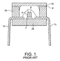
- a conventional solid state pickup device is a CCD device and comprises a pair of lead terminal-lines or terminal-groups 1b and 1c provided with a plurality of lead terminals arranged in parallel to one another in a direction perpendicular to the sheet surface of Fig.
- a base portion 2a made of opaque epoxies-resin
- a CCD chip 3 glued (die-bonded) on the base portion 2a by adhesive 7 made of silicone-compound
- a plurality of bonding-wires 4 bonded between the terminal-lines 1b and 1c and the CCD chip 3, respectively, a cylindrical wall portion 2b made of opacity epoxies-resin and integrally formed on the base portion 2a through the terminal-lines 1b and 1c
- a top plate 10 made of transparent resin and glued on an upper end of the cylindrical wall portion 2b by transparent adhesive 8 can be set or cured by ultraviolet-curing.
- the base portion 2a and the cylindrical wall portion 2b may be molded individually.
- the base portion 2a, the cylindrical wall portion 2b, and the top plate 10 cooperate to serve as a package of the CCD device.
- the CCD device of the package type mentioned above is called a hollow-molded CCD device because a space is left in the package.
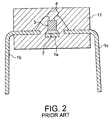
- the other conventional solid state pickup device is also a CCD device.
- the CCD device comprises a pair of lead terminal-lines or terminal-groups 1b and 1c provided with a plurality of lead terminals arranged in parallel to one another in a direction perpendicular to the sheet surface of Fig.
- the CCD device of the package type mentioned above is called a solid-molded CCD device because full molded by the solid package so that all the members are molded.
- the CCD device is manufactured as follows.
- a lead frame (not shown), which comprises the terminal-lines 1b and 1 and the island member 1a connected to one another by a peripheral frame as the extra member, is prepared.
- the CCD chip 3 is die-bonded on the island 1a by the adhesive 7.
- the bonding-wires 4 are bonded between the terminal-lines 1b and 1c and the CCD chip 3, respectively.
- the lead frame is set in a casting mold not shown. Molten transparent resin can be set or cured by thermosetting or photosetting is poured into the casting mold. The melted resin is set or cured by heating and therefore is formed as the solid package 11. The solid package 11 is taken out from the casting mold. The peripheral frame is removed from the lead frame. Thus, the solid-molded CCD device is completed.
- the conventional CCD devices have problems described in the preamble.
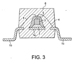
- a solid state pickup device is also a solid-molded CCD device.
- the solid-molded CCD device of this embodiment has similar parts designated by the same reference numerals that are illustrated in Fig. 2.
- the solid-molded CCD device comprises a pair of lead terminal-lines or terminal-groups 1b and 1c provided with a plurality of lead terminals arranged in parallel to one another in a direction perpendicular to the sheet surface of Fig. 3, respectively, an island member 1a connected to the terminal-lines 1b and 1c by an extra member (not shown) before the device is completed, a CCD chip 3 glued (die-bonded) on the island member 1a by adhesive 7 made of silicone-compound having flexibility, a plurality of bonding-wires 4 bonded between the terminal-lines 1b and 1c and connection pattern (not shown) formed on a top surface as a receiving surface of the CCD chip 3, respectively, a covering member 5 made of transparent resin having flexibility formed around the top surface and the side surfaces of the CCD chip 3, and a solid package 6 made of transparent resin can be set or cured by thermosetting or photosetting and formed (molded) so as to cover the terminal-lines 1b and 1c, the island member 1a, the CCD chip 3 covered with the covering
- the CCD chip 3 is isolated from the island member 1a and the solid package 6 through the adhesive 7 and the covering member 5 with a bottom surface, the side surfaces, and the top surface thereof not exposed to the island member 1a and the solid package 6.
- Fig. 4 shows a lead frame 1 used for manufacturing the solid-molded CCD device.
- the frame 1 also serves as the island member 1a and the terminal-lines 1b and 1c when the device is completed.
- the lead frame 1 is made by punching out a metal plate made of ferroalloy or copper alloy and plating the punched plate with metal.
- the island member 1a serves to mount the CCD chip 3 thereon.
- the adhesive 7 is dispensed from a dispenser of the adhesive and which is spread on the island member 1a. It is preferred that the adhesive 7 is elastic, flexible, or sticky material like gum or jelly and which is not lower than 300 °C in temporary heat-resistance.
- the adhesive 7 is made of silicone resin, polyurethane resin, rubber, and so on.
- the CCD chip 3 is mounted on the island member 1a through the adhesive 7.
- the lead frame 1 with the CCD chip 3 mounted thereon is put into a homoiothermic tank.
- the homoiothermic tank is controlled so that an inner temperature therein is maintained between 80 and 180 °C.
- the adhesive 7 is set or cured but which has flexibility.
- the bonding-wires 4 are bonded between the terminal-lines 1b and 1c and the connection patterns formed on the receiving (top) surface of the CCD chip 3, respectively.
- the transparent resin is dispensed from a dispenser of the resin onto the top and the side surfaces of the CCD chip 3 and a top surface of the island 1a except an area for mounting the CCD chip 3 thereon.
- the covering member 5 made of the transparent resin is formed around the top and the side surfaces of the CCD chip 3 and the area of the island 1a.
- the covering member 5 has flexibility.
- the transparent resin resin of thermosetting or photosetting type is prepared and used.
- the resin has liquid form before set or cured and which is slight in reaction when set or cured. Namely, the resin is spread flatly with spreading thickness constant before set or cured while will not less than 20 ⁇ m in set thickness thereof after set or cured. Furthermore, it is preferred that the resin is elastic, flexible, or sticky like gum or jelly and which is not lower than 300 °C in temporary heat-resistance after set or cured.
- silicone resin or polyurethane resin added a little drizzly-silica and provided with reaction property little is preferred as the thermosetting or the photosetting resin.
- the lead frame 1 is put into the homoiothermic tank controlled so that the inner temperature therein is maintained between 80 and 180 °C or an ultraviolet-curing furnace for applying ultraviolet rays to the resin.
- the solid package 6 is formed (molded) so as to cover the island member 1a, the CCD chip 3 covered with the covering member 5, and the bonding-wires 4 therein by a transfer-molding.
- the solid package 6 is transparent and which is formed by the transfer-molding.
- the transparent resin becomes the solid package 6 which is rigid with Shore-D hardness not less than 80 after set or cured by the transfer-molding.
- a resin capable of being set or cured by thermosetting or photosetting may be used as the transparent resin.
- Portions sticking out from the solid package 6 of the terminal-lines 1b and 1c are bent into prescribed forms, respectively. Furthermore, the peripheral frame of the lead frame 1 is cut away. Thus, the solid-molded CCD device is completed.
- All component members or pieces of the solid-molded CCD device are not lower than 300 °C in at least temporary heat-resistance.
- the covering member covering the CCD chip without space or aperture left therebetween is transparent and which is between 0 and 30 in hardness (a rubber hardness standardized in JIS-A).
- the solid-molded CCD device completed as mentioned above is applied to the reflow-soldering process, the solid-molded CCD device is cooled after heated between 260 and 300 °C.
- the component members of the device such as the is land member 1a, the terminal-lines 1b and 1c, the CCD chip 3, and the solid package 6 shown in Fig. 2 are inconsistently expanded and shrunk according to inconsistent heat-expansion coefficients, respectively. Therefore, the component members are stressed to one another.
- the solid package 6 is shrunk remarkably and irreversibly after cooled and therefore stresses itself and other component members remarkably and irreversibly.
- the solid package 6 stressed may be deformed and cracked.
- the solid package 6 may be also deteriorated in flatness and therefore may interfere with the optical signal traveled to the CCD chip 3.
- the covering member 5 and the adhesive 7 are shrunk by stresses of the component members and therefore absorb the stresses and prevent the stresses from traveling to the CCD chip 3 because flexible.
- the CCD chip 3 is not stressed, deformed, and cracked.
- the solid package 6 is not stressed, deformed, cracked, and deteriorated in flatness although shrunk remarkably and irreversibly. Therefore, the solid package 6 does not interfere with the optical signal traveled to the CCD chip 3.
- the lead frame 1 shown in Fig. 4 is prepared. Namely, A sheet made of copper alloy between 0.15 and 0.25 mm in thickness is prepared. The sheet metal is pressed into a form shown in Fig. 4. The pressed metal is plated with a noble metal such as gold, silver, palladium, or rhodium between 0.004 and 0.500 ⁇ m in thickness. Thus, the lead frame 1 is completed.
- a noble metal such as gold, silver, palladium, or rhodium between 0.004 and 0.500 ⁇ m in thickness.
- Silicone compound serving as the adhesive 7 is prepared.
- the silicone compound is approximately 100 p (where the device is Poise) in viscosity before set or cured while between 0 and 30 in hardness (the rubber hardness standardized in JIS-A) after set or cured by heating between 150 and 200 °C.
- the silicone compound is dispensed from the dispenser and which is spread on the island member 1a.
- the CCD chip 3 is mounted on the island member 1a through the silicone compound.
- the lead frame 1 with the CCD chip 3 mounted thereon is put into a homoiothermic tank.
- the homoiothermic tank is controlled so that an inner temperature therein is maintained between 80 and 180 °C.
- the adhesive 7 is set or cured but which has flexibility with Shore-D hardness between 20 and 30.
- the bonding-wires 4 are bonded between the terminal-lines 1b and 1c and the connection patterns formed on the receiving (top) surface of the CCD chip 3, respectively.
- Silicone compound of thermosetting-type for making the covering member 5 is prepared.
- the silicone compound is between 20 and 40 p in viscosity and which is between 1.0 and 1.2 in thixotropic factor before set or cured while 0 in Shore-A hardness and not less than 90% in transparency after set or cured by heating between 150 and 200 °C.
- the silicone compound is dispensed from the dispenser over the CCD chip 3 so that the top and the side surfaces thereof and a top surface of the island 1a except an area mounting the CCD chip 3 thereof are covered with the compound.
- the lead frame 1 with the CCD chip 3 mounted thereon and covered with the compound is put into a homoiothermic tank.
- the homoiothermic tank is controlled so that an inner temperature therein is maintained between 150 and 200 °C.
- the covering member 5 with the transparency 90% is thus set or cured but which has flexibility with Shore-A hardness 0.
- the covering member 5 is formed around the top and the side surfaces of the CCD chip 3 and the area of the island 1a.
- Resin of thermosetting-type for making the solid package 6 is prepared.
- the resin consists essentially of epoxy resin of epi-bis- or bis-epi- type such as bisphenol-epichlorohydrin epoxy resin as main agent, hexahydrophthalic anhydride serving as the hardening agent and sub agent, and traces of curing acceleration agent, mold release agent, surface treatment agent, and other agents as the balances. After the resin is set or cured by heating between 80 and 180 °C, the resin is approximately 85 in Shore-D hardness and approximately 92% in transparency.
- the resin is formed or molded so as to cover the island member 1a, the CCD chip 3 covered with the covering member 5, and the bonding-wires 4 therein.
- the molded resin serves as the solid package 6.
- the solid package 6 is 92% in transparency and which is rigid.
- Portions of the terminal-lines 1b and 1c sticking out from the solid package 6 are bent into prescribed forms, respectively. Furthermore, the peripheral frame of the lead frame 1 is cut away. Thus, the solid-molded CCD device is completed.
- a top surface of the resin for forming the solid package 6 is often uneven after the transfer-molding.
- the reason is that the lead frame 1 is uneven and has slits or hole in many portions thereof.
- Another reason is why the resin is shrunk and cured in inconsistent rates at many areas thereof.
- a second embodiment of the present invention serves to improve the above-mentioned problem.
- a solid state pickup device is also a solid-molded CCD device.
- the solid-molded CCD device of this embodiment has similar parts designated by the same reference numerals that are illustrated in Fig. 3 about the first embodiment.
- the solid-molded CCD device further comprises a top plate 20 formed or attached on a top surface 6a of the solid package 6 through an adhesive 18.
- the top plate 20 is transparent, rigid, and tensional like glass.
- the adhesive 18 can be set or cured by ultraviolet-curing and which is transparent and flexible.
- the top plate 20 is attached to the top surface 6a of the solid package 6 by the following manner.
- the adhesive 18 a transparent adhesive of urethane acrylate-series is prepared.
- the adhesive 18 will be between 40 and 50 in Shore-D hardness after cured or set.
- the top plate 20 is prepared.
- the top plate is made of plastic selected from acrylic acid resin, polycarbonate, and polyether sulfonic acid of norbornane-series while made of borosilicate glass and so on.
- the adhesive 18 is spread over the top surface 6a of the solid package 6.
- the top plate 20 is mounted on the top surface 6a through the adhesive 18.
- the adhesive 18 is irradiated through the top plate 20 by ultraviolet rays not less than 3000 mJ/cm 2 output from a high pressure mercury vapour lamp or a metal halide lamp and which is thus cured but flexible such that Shore-D hardness between 40 and 50.
- ultraviolet rays not less than 3000 mJ/cm 2 output from a high pressure mercury vapour lamp or a metal halide lamp and which is thus cured but flexible such that Shore-D hardness between 40 and 50.
- a top surface of the top plate 20 serving as a top surface of the device is flat if the top surface 6a of the solid package 6 is uneven after the transfer-molding. Therefore, the solid-molded CCD device is excellent in optical and electrical performances because the device can receive the light signal without refracting and diffused-reflecting the light signal. Furthermore, if the top plate 20 and the solid package 6 are different in the expansion or a shrinkage coefficient to each other, these members are not stressed to each other because the stresses are absorbed by the adhesive 18.
- the present invention is capable of applying to another solid state pickup device such as a device using a CMOS (a Complementary Metal-Oxide Semiconductor) chip instead of the CCD chip.
- CMOS Complementary Metal-Oxide Semiconductor
- the present invention is capable of adopting flexible members made of various materials instead of gum-like and jelly-like resins as the covering member.
Landscapes
- Engineering & Computer Science (AREA)
- Microelectronics & Electronic Packaging (AREA)
- Physics & Mathematics (AREA)
- Power Engineering (AREA)
- Condensed Matter Physics & Semiconductors (AREA)
- Electromagnetism (AREA)
- General Physics & Mathematics (AREA)
- Computer Hardware Design (AREA)
- Solid State Image Pick-Up Elements (AREA)
- Structures Or Materials For Encapsulating Or Coating Semiconductor Devices Or Solid State Devices (AREA)
- Transforming Light Signals Into Electric Signals (AREA)
Applications Claiming Priority (2)
| Application Number | Priority Date | Filing Date | Title |
|---|---|---|---|
| JP7974198 | 1998-03-26 | ||
| JP07974198A JP3173586B2 (ja) | 1998-03-26 | 1998-03-26 | 全モールド型固体撮像装置およびその製造方法 |
Publications (2)
| Publication Number | Publication Date |
|---|---|
| EP0949675A2 true EP0949675A2 (de) | 1999-10-13 |
| EP0949675A3 EP0949675A3 (de) | 2000-04-19 |
Family
ID=13698654
Family Applications (1)
| Application Number | Title | Priority Date | Filing Date |
|---|---|---|---|
| EP99106060A Withdrawn EP0949675A3 (de) | 1998-03-26 | 1999-03-25 | Hitzbeständige Festkörperbildaufnahmevorrichtung und Verfahren zu ihrer Herstellung |
Country Status (5)
| Country | Link |
|---|---|
| US (1) | US6144107A (de) |
| EP (1) | EP0949675A3 (de) |
| JP (1) | JP3173586B2 (de) |
| KR (1) | KR100293138B1 (de) |
| CN (1) | CN1129964C (de) |
Families Citing this family (21)
| Publication number | Priority date | Publication date | Assignee | Title |
|---|---|---|---|---|
| US6008074A (en) | 1998-10-01 | 1999-12-28 | Micron Technology, Inc. | Method of forming a synchronous-link dynamic random access memory edge-mounted device |
| US6753922B1 (en) * | 1998-10-13 | 2004-06-22 | Intel Corporation | Image sensor mounted by mass reflow |
| US6452268B1 (en) * | 2000-04-26 | 2002-09-17 | Siliconware Precision Industries Co., Ltd. | Integrated circuit package configuration having an encapsulating body with a flanged portion and an encapsulating mold for molding the encapsulating body |
| US6629633B1 (en) | 2000-11-13 | 2003-10-07 | Amkor Technology, Inc. | Chip size image sensor bumped package fabrication method |
| US6620646B1 (en) | 2000-11-13 | 2003-09-16 | Amkor Technology, Inc. | Chip size image sensor wirebond package fabrication method |
| US6509560B1 (en) | 2000-11-13 | 2003-01-21 | Amkor Technology, Inc. | Chip size image sensor in wirebond package with step-up ring for electrical contact |
| US6528857B1 (en) * | 2000-11-13 | 2003-03-04 | Amkor Technology, Inc. | Chip size image sensor bumped package |
| US7122908B2 (en) * | 2001-02-01 | 2006-10-17 | Micron Technology, Inc. | Electronic device package |
| US6603183B1 (en) * | 2001-09-04 | 2003-08-05 | Amkor Technology, Inc. | Quick sealing glass-lidded package |
| US6759266B1 (en) | 2001-09-04 | 2004-07-06 | Amkor Technology, Inc. | Quick sealing glass-lidded package fabrication method |
| US6512286B1 (en) * | 2001-10-09 | 2003-01-28 | Siliconware Precision Industries Co., Ltd. | Semiconductor package with no void in encapsulant and method for fabricating the same |
| JP3934648B2 (ja) * | 2002-05-15 | 2007-06-20 | 松下電器産業株式会社 | 光検出器、光ヘッド装置、光情報処理装置および光情報処理方法 |
| US7262074B2 (en) * | 2002-07-08 | 2007-08-28 | Micron Technology, Inc. | Methods of fabricating underfilled, encapsulated semiconductor die assemblies |
| US20050098710A1 (en) * | 2003-11-10 | 2005-05-12 | Jackson Hsieh | Image sensor package |
| TWI275189B (en) * | 2003-12-30 | 2007-03-01 | Osram Opto Semiconductors Gmbh | Radiation-emitting and/or radiation-receiving semiconductor component and method for producing such component |
| JP2005217322A (ja) * | 2004-01-30 | 2005-08-11 | Toshiba Corp | 固体撮像装置用半導体素子とそれを用いた固体撮像装置 |
| KR100592368B1 (ko) * | 2004-07-06 | 2006-06-22 | 삼성전자주식회사 | 반도체 소자의 초박형 모듈 제조 방법 |
| JP2006237105A (ja) * | 2005-02-23 | 2006-09-07 | Tdk Corp | 電子部品およびその製造方法 |
| JP2007173496A (ja) * | 2005-12-22 | 2007-07-05 | Matsushita Electric Ind Co Ltd | 固体撮像素子用パッケージおよび固体撮像装置 |
| JP2009016405A (ja) * | 2007-06-30 | 2009-01-22 | Zycube:Kk | 固体撮像装置 |
| JP2009049218A (ja) * | 2007-08-21 | 2009-03-05 | Nec Electronics Corp | 半導体装置及び半導体装置の製造方法 |
Family Cites Families (13)
| Publication number | Priority date | Publication date | Assignee | Title |
|---|---|---|---|---|
| JPS59167037A (ja) * | 1983-03-14 | 1984-09-20 | Oki Electric Ind Co Ltd | 半導体装置 |
| DE3782201T2 (de) * | 1986-07-16 | 1993-04-15 | Canon Kk | Halbleiterphotosensor und verfahren zu dessen herstellung. |
| JPH0750758B2 (ja) * | 1987-01-30 | 1995-05-31 | 株式会社日立製作所 | 耐熱性樹脂封止半導体装置 |
| JPS63269554A (ja) * | 1987-04-27 | 1988-11-07 | Mitsubishi Electric Corp | 半導体装置 |
| JPS63269557A (ja) * | 1987-04-27 | 1988-11-07 | Nec Corp | リ−ドフレ−ム |
| JPH03116857A (ja) * | 1989-09-29 | 1991-05-17 | Mitsui Petrochem Ind Ltd | 発光または受光装置 |
| JP2974700B2 (ja) * | 1989-11-30 | 1999-11-10 | 東レ・ダウコーニング・シリコーン株式会社 | 導電性接着剤 |
| EP0509065A1 (de) * | 1990-08-01 | 1992-10-21 | Staktek Corporation | Gehäuse für integrierte schaltung von ultrahoher dichte, verfahren und gerät |
| JPH0797652B2 (ja) * | 1990-11-28 | 1995-10-18 | 浜松ホトニクス株式会社 | 受光素子 |
| JP2533001B2 (ja) * | 1991-02-27 | 1996-09-11 | 三洋電機株式会社 | 固体撮像素子の製造方法 |
| KR960009089B1 (ko) * | 1993-03-04 | 1996-07-10 | 문정환 | 패키지 성형용 금형 및 그 금형을 이용한 플라스틱 고체촬상소자 패키지 제조방법 및 패키지 |
| US5557066A (en) * | 1993-04-30 | 1996-09-17 | Lsi Logic Corporation | Molding compounds having a controlled thermal coefficient of expansion, and their uses in packaging electronic devices |
| JPH08335720A (ja) * | 1995-06-08 | 1996-12-17 | Nichia Chem Ind Ltd | 窒化物半導体発光ダイオード |
-
1998
- 1998-03-26 JP JP07974198A patent/JP3173586B2/ja not_active Expired - Fee Related
-
1999
- 1999-03-25 EP EP99106060A patent/EP0949675A3/de not_active Withdrawn
- 1999-03-25 US US09/275,822 patent/US6144107A/en not_active Expired - Lifetime
- 1999-03-26 KR KR1019990010642A patent/KR100293138B1/ko not_active IP Right Cessation
- 1999-03-26 CN CN99104426A patent/CN1129964C/zh not_active Expired - Fee Related
Also Published As
| Publication number | Publication date |
|---|---|
| US6144107A (en) | 2000-11-07 |
| CN1230782A (zh) | 1999-10-06 |
| JP3173586B2 (ja) | 2001-06-04 |
| EP0949675A3 (de) | 2000-04-19 |
| KR19990078327A (ko) | 1999-10-25 |
| CN1129964C (zh) | 2003-12-03 |
| JPH11274447A (ja) | 1999-10-08 |
| KR100293138B1 (ko) | 2001-06-15 |
Similar Documents
| Publication | Publication Date | Title |
|---|---|---|
| US6144107A (en) | Solid state pickup device excellent in heat-resistance and method of manufacturing the device | |
| US5081520A (en) | Chip mounting substrate having an integral molded projection and conductive pattern | |
| EP0561964B1 (de) | Packung für eine optoelektronische vorrichtung und verfahren zu ihrer herstellung | |
| EP0682374B1 (de) | Verfahren zur Einkapselung einer integrierten Schaltung | |
| EP0591862B1 (de) | Halbleitervorrichtung, Bildabtastvorrichtung und Verfahren zu ihrer Herstellung | |
| US5647122A (en) | Manufacturing method for an integrated circuit card | |
| CN100438023C (zh) | 摄像模块及其制造方法 | |
| US6964886B2 (en) | Methods of fabrication for flip-chip image sensor packages | |
| US4957882A (en) | Method for manufacturing semiconductor device | |
| US5998862A (en) | Air-packed CCD images package and a mold for manufacturing thereof | |
| JP3630447B2 (ja) | 固体撮像素子の製造方法 | |
| KR100758055B1 (ko) | 광전자장치 및 그 제조방법 | |
| US20130241020A1 (en) | Solid image-pickup device with flexible circuit substrate | |
| US7998781B2 (en) | Method of manufacturing semiconductor device in which functional portion of element is exposed | |
| EP1473775B1 (de) | Verfahren zur Herstellung einer Festkörper-Bildaufnahmevorrichtung | |
| JP2966591B2 (ja) | 光半導体装置 | |
| SE515880C2 (sv) | Sätt att tillverka en optisk kopplingsenhet | |
| JP3127584B2 (ja) | 樹脂製中空パッケージを用いた半導体装置 | |
| KR20020006343A (ko) | 반도체 패키지 및 그 제조방법 | |
| JPH05291546A (ja) | 固体撮像素子の製造方法 | |
| JP3238256B2 (ja) | 半導体装置、イメージセンサ装置及びそれらの製造方法 | |
| JP3340455B2 (ja) | Oリングパッケージ | |
| NL9400508A (nl) | Werkwijze voor het monteren van elektronische componenten middels solderbumps en toepassingen en voortbrengselen hiervan. | |
| JP3682756B2 (ja) | 半導体装置 | |
| JP2674513B2 (ja) | フォトカプラ |
Legal Events
| Date | Code | Title | Description |
|---|---|---|---|
| PUAI | Public reference made under article 153(3) epc to a published international application that has entered the european phase |
Free format text: ORIGINAL CODE: 0009012 |
|
| AK | Designated contracting states |
Kind code of ref document: A2 Designated state(s): DE FR GB NL |
|
| AX | Request for extension of the european patent |
Free format text: AL;LT;LV;MK;RO;SI |
|
| PUAL | Search report despatched |
Free format text: ORIGINAL CODE: 0009013 |
|
| AK | Designated contracting states |
Kind code of ref document: A3 Designated state(s): AT BE CH CY DE DK ES FI FR GB GR IE IT LI LU MC NL PT SE |
|
| AX | Request for extension of the european patent |
Free format text: AL;LT;LV;MK;RO;SI |
|
| RIC1 | Information provided on ipc code assigned before grant |
Free format text: 7H 01L 23/31 A, 7H 01L 31/0203 B |
|
| 17P | Request for examination filed |
Effective date: 20000313 |
|
| AKX | Designation fees paid |
Free format text: DE FR GB NL |
|
| 17Q | First examination report despatched |
Effective date: 20010216 |
|
| RAP1 | Party data changed (applicant data changed or rights of an application transferred) |
Owner name: NEC ELECTRONICS CORPORATION |
|
| STAA | Information on the status of an ep patent application or granted ep patent |
Free format text: STATUS: THE APPLICATION IS DEEMED TO BE WITHDRAWN |
|
| 18D | Application deemed to be withdrawn |
Effective date: 20030127 |