EP0938747B1 - Regulierbarer, hochtemperatur-halter für plasma-cvd einer hohen dichte - Google Patents
Regulierbarer, hochtemperatur-halter für plasma-cvd einer hohen dichte Download PDFInfo
- Publication number
- EP0938747B1 EP0938747B1 EP97943648A EP97943648A EP0938747B1 EP 0938747 B1 EP0938747 B1 EP 0938747B1 EP 97943648 A EP97943648 A EP 97943648A EP 97943648 A EP97943648 A EP 97943648A EP 0938747 B1 EP0938747 B1 EP 0938747B1
- Authority
- EP
- European Patent Office
- Prior art keywords
- electrostatic chuck
- electrode cap
- set forth
- electrode
- cap
- Prior art date
- Legal status (The legal status is an assumption and is not a legal conclusion. Google has not performed a legal analysis and makes no representation as to the accuracy of the status listed.)
- Expired - Lifetime
Links
- 238000005229 chemical vapour deposition Methods 0.000 title description 2
- 238000010438 heat treatment Methods 0.000 claims abstract description 30
- 239000002826 coolant Substances 0.000 claims abstract description 25
- 239000007788 liquid Substances 0.000 claims abstract description 22
- 239000007789 gas Substances 0.000 claims description 18
- LYCAIKOWRPUZTN-UHFFFAOYSA-N Ethylene glycol Chemical compound OCCO LYCAIKOWRPUZTN-UHFFFAOYSA-N 0.000 claims description 13
- 239000000919 ceramic Substances 0.000 claims description 12
- 239000001307 helium Substances 0.000 claims description 11
- 229910052734 helium Inorganic materials 0.000 claims description 11
- SWQJXJOGLNCZEY-UHFFFAOYSA-N helium atom Chemical compound [He] SWQJXJOGLNCZEY-UHFFFAOYSA-N 0.000 claims description 11
- XAGFODPZIPBFFR-UHFFFAOYSA-N aluminium Chemical compound [Al] XAGFODPZIPBFFR-UHFFFAOYSA-N 0.000 claims description 9
- PMHQVHHXPFUNSP-UHFFFAOYSA-M copper(1+);methylsulfanylmethane;bromide Chemical compound Br[Cu].CSC PMHQVHHXPFUNSP-UHFFFAOYSA-M 0.000 claims description 9
- 229910052782 aluminium Inorganic materials 0.000 claims description 8
- 229910003460 diamond Inorganic materials 0.000 claims description 8
- 239000010432 diamond Substances 0.000 claims description 8
- ZOKXTWBITQBERF-UHFFFAOYSA-N Molybdenum Chemical compound [Mo] ZOKXTWBITQBERF-UHFFFAOYSA-N 0.000 claims description 6
- 229910052750 molybdenum Inorganic materials 0.000 claims description 6
- 239000011733 molybdenum Substances 0.000 claims description 6
- XKRFYHLGVUSROY-UHFFFAOYSA-N Argon Chemical compound [Ar] XKRFYHLGVUSROY-UHFFFAOYSA-N 0.000 claims description 4
- RVZRBWKZFJCCIB-UHFFFAOYSA-N perfluorotributylamine Chemical compound FC(F)(F)C(F)(F)C(F)(F)C(F)(F)N(C(F)(F)C(F)(F)C(F)(F)C(F)(F)F)C(F)(F)C(F)(F)C(F)(F)C(F)(F)F RVZRBWKZFJCCIB-UHFFFAOYSA-N 0.000 claims description 3
- XUIMIQQOPSSXEZ-UHFFFAOYSA-N Silicon Chemical compound [Si] XUIMIQQOPSSXEZ-UHFFFAOYSA-N 0.000 claims description 2
- 229910052786 argon Inorganic materials 0.000 claims description 2
- 239000000203 mixture Substances 0.000 claims description 2
- 239000003921 oil Substances 0.000 claims description 2
- 229910052710 silicon Inorganic materials 0.000 claims description 2
- 239000010703 silicon Substances 0.000 claims description 2
- IJGRMHOSHXDMSA-UHFFFAOYSA-N Atomic nitrogen Chemical compound N#N IJGRMHOSHXDMSA-UHFFFAOYSA-N 0.000 claims 2
- 239000008367 deionised water Substances 0.000 claims 2
- QVGXLLKOCUKJST-UHFFFAOYSA-N atomic oxygen Chemical compound [O] QVGXLLKOCUKJST-UHFFFAOYSA-N 0.000 claims 1
- 229910052757 nitrogen Inorganic materials 0.000 claims 1
- TWNQGVIAIRXVLR-UHFFFAOYSA-N oxo(oxoalumanyloxy)alumane Chemical compound O=[Al]O[Al]=O TWNQGVIAIRXVLR-UHFFFAOYSA-N 0.000 claims 1
- 239000001301 oxygen Substances 0.000 claims 1
- 229910052760 oxygen Inorganic materials 0.000 claims 1
- 238000001816 cooling Methods 0.000 abstract description 17
- 239000004065 semiconductor Substances 0.000 abstract description 9
- 238000012546 transfer Methods 0.000 abstract description 2
- 235000012431 wafers Nutrition 0.000 description 51
- 238000012545 processing Methods 0.000 description 14
- 239000012212 insulator Substances 0.000 description 12
- 239000011248 coating agent Substances 0.000 description 11
- 238000000576 coating method Methods 0.000 description 11
- 238000004891 communication Methods 0.000 description 5
- 239000011888 foil Substances 0.000 description 5
- 238000000034 method Methods 0.000 description 5
- 239000010445 mica Substances 0.000 description 5
- 229910052618 mica group Inorganic materials 0.000 description 5
- PNEYBMLMFCGWSK-UHFFFAOYSA-N aluminium oxide Inorganic materials [O-2].[O-2].[O-2].[Al+3].[Al+3] PNEYBMLMFCGWSK-UHFFFAOYSA-N 0.000 description 4
- 230000008901 benefit Effects 0.000 description 4
- 229910010293 ceramic material Inorganic materials 0.000 description 4
- 238000000151 deposition Methods 0.000 description 4
- 230000008021 deposition Effects 0.000 description 4
- 230000008569 process Effects 0.000 description 4
- XLYOFNOQVPJJNP-UHFFFAOYSA-N water Substances O XLYOFNOQVPJJNP-UHFFFAOYSA-N 0.000 description 4
- 238000002048 anodisation reaction Methods 0.000 description 3
- 238000013461 design Methods 0.000 description 3
- 210000002304 esc Anatomy 0.000 description 3
- 239000007921 spray Substances 0.000 description 3
- 229910052582 BN Inorganic materials 0.000 description 2
- PZNSFCLAULLKQX-UHFFFAOYSA-N Boron nitride Chemical compound N#B PZNSFCLAULLKQX-UHFFFAOYSA-N 0.000 description 2
- VYPSYNLAJGMNEJ-UHFFFAOYSA-N Silicium dioxide Chemical group O=[Si]=O VYPSYNLAJGMNEJ-UHFFFAOYSA-N 0.000 description 2
- 239000002131 composite material Substances 0.000 description 2
- 239000000110 cooling liquid Substances 0.000 description 2
- 230000001351 cycling effect Effects 0.000 description 2
- -1 for example Substances 0.000 description 2
- WGCNASOHLSPBMP-UHFFFAOYSA-N hydroxyacetaldehyde Natural products OCC=O WGCNASOHLSPBMP-UHFFFAOYSA-N 0.000 description 2
- 238000003754 machining Methods 0.000 description 2
- 238000004519 manufacturing process Methods 0.000 description 2
- 238000005240 physical vapour deposition Methods 0.000 description 2
- 230000001681 protective effect Effects 0.000 description 2
- 229910000838 Al alloy Inorganic materials 0.000 description 1
- 229910000831 Steel Inorganic materials 0.000 description 1
- 239000004809 Teflon Substances 0.000 description 1
- 229920006362 Teflon® Polymers 0.000 description 1
- 238000009529 body temperature measurement Methods 0.000 description 1
- 230000015556 catabolic process Effects 0.000 description 1
- 229910052681 coesite Inorganic materials 0.000 description 1
- 239000000112 cooling gas Substances 0.000 description 1
- 238000005336 cracking Methods 0.000 description 1
- 229910052906 cristobalite Inorganic materials 0.000 description 1
- 238000010586 diagram Methods 0.000 description 1
- 238000009826 distribution Methods 0.000 description 1
- 230000005684 electric field Effects 0.000 description 1
- 238000005530 etching Methods 0.000 description 1
- 239000012530 fluid Substances 0.000 description 1
- 230000004907 flux Effects 0.000 description 1
- 238000009413 insulation Methods 0.000 description 1
- 239000000463 material Substances 0.000 description 1
- 229910001120 nichrome Inorganic materials 0.000 description 1
- 230000037361 pathway Effects 0.000 description 1
- 238000000623 plasma-assisted chemical vapour deposition Methods 0.000 description 1
- 230000010287 polarization Effects 0.000 description 1
- 239000000523 sample Substances 0.000 description 1
- 238000000926 separation method Methods 0.000 description 1
- 239000000377 silicon dioxide Substances 0.000 description 1
- 239000010935 stainless steel Substances 0.000 description 1
- 229910001220 stainless steel Inorganic materials 0.000 description 1
- 239000010959 steel Substances 0.000 description 1
- 229910052682 stishovite Inorganic materials 0.000 description 1
- 239000000758 substrate Substances 0.000 description 1
- 230000001052 transient effect Effects 0.000 description 1
- 229910052905 tridymite Inorganic materials 0.000 description 1
- 239000011800 void material Substances 0.000 description 1
Images


Classifications
-
- H—ELECTRICITY
- H01—ELECTRIC ELEMENTS
- H01L—SEMICONDUCTOR DEVICES NOT COVERED BY CLASS H10
- H01L21/00—Processes or apparatus adapted for the manufacture or treatment of semiconductor or solid state devices or of parts thereof
- H01L21/67—Apparatus specially adapted for handling semiconductor or electric solid state devices during manufacture or treatment thereof; Apparatus specially adapted for handling wafers during manufacture or treatment of semiconductor or electric solid state devices or components ; Apparatus not specifically provided for elsewhere
- H01L21/68—Apparatus specially adapted for handling semiconductor or electric solid state devices during manufacture or treatment thereof; Apparatus specially adapted for handling wafers during manufacture or treatment of semiconductor or electric solid state devices or components ; Apparatus not specifically provided for elsewhere for positioning, orientation or alignment
-
- H—ELECTRICITY
- H01—ELECTRIC ELEMENTS
- H01L—SEMICONDUCTOR DEVICES NOT COVERED BY CLASS H10
- H01L21/00—Processes or apparatus adapted for the manufacture or treatment of semiconductor or solid state devices or of parts thereof
- H01L21/67—Apparatus specially adapted for handling semiconductor or electric solid state devices during manufacture or treatment thereof; Apparatus specially adapted for handling wafers during manufacture or treatment of semiconductor or electric solid state devices or components ; Apparatus not specifically provided for elsewhere
- H01L21/683—Apparatus specially adapted for handling semiconductor or electric solid state devices during manufacture or treatment thereof; Apparatus specially adapted for handling wafers during manufacture or treatment of semiconductor or electric solid state devices or components ; Apparatus not specifically provided for elsewhere for supporting or gripping
- H01L21/6831—Apparatus specially adapted for handling semiconductor or electric solid state devices during manufacture or treatment thereof; Apparatus specially adapted for handling wafers during manufacture or treatment of semiconductor or electric solid state devices or components ; Apparatus not specifically provided for elsewhere for supporting or gripping using electrostatic chucks
-
- H—ELECTRICITY
- H01—ELECTRIC ELEMENTS
- H01L—SEMICONDUCTOR DEVICES NOT COVERED BY CLASS H10
- H01L21/00—Processes or apparatus adapted for the manufacture or treatment of semiconductor or solid state devices or of parts thereof
- H01L21/67—Apparatus specially adapted for handling semiconductor or electric solid state devices during manufacture or treatment thereof; Apparatus specially adapted for handling wafers during manufacture or treatment of semiconductor or electric solid state devices or components ; Apparatus not specifically provided for elsewhere
- H01L21/67005—Apparatus not specifically provided for elsewhere
- H01L21/67011—Apparatus for manufacture or treatment
- H01L21/67098—Apparatus for thermal treatment
- H01L21/67109—Apparatus for thermal treatment mainly by convection
-
- Y—GENERAL TAGGING OF NEW TECHNOLOGICAL DEVELOPMENTS; GENERAL TAGGING OF CROSS-SECTIONAL TECHNOLOGIES SPANNING OVER SEVERAL SECTIONS OF THE IPC; TECHNICAL SUBJECTS COVERED BY FORMER USPC CROSS-REFERENCE ART COLLECTIONS [XRACs] AND DIGESTS
- Y10—TECHNICAL SUBJECTS COVERED BY FORMER USPC
- Y10T—TECHNICAL SUBJECTS COVERED BY FORMER US CLASSIFICATION
- Y10T279/00—Chucks or sockets
- Y10T279/23—Chucks or sockets with magnetic or electrostatic means
Definitions
- the present invention relates to an electrostatic chuck (ESC) for holding a work object. More particularly, it relates to an electrostatic chuck with active temperature control, for holding and controlling the temperature of a semiconductor wafer during integrated circuit fabrication.
- ESC electrostatic chuck
- a number of different chucks are widely used to hold semiconductor wafers during processing.
- Mechanical chucks can secure the wafer by using arms or clamps to press the wafer against a supporting surface.
- the clamping force is inherently non-uniform, resulting in uneven stresses in the wafer which can cause deformation, and uneven thermal contact between the wafer and the support.
- Vacuum chucks secure the wafer by evacuating a void beneath the wafer backside, thereby generating a clamping force due to the pressure differential between the processing chamber and the wafer backside.
- Vacuum chucks can provide a more uniform clamping force than can mechanical chucks, but in the low pressure environments required for many semiconductor processing applications, the pressure differential is insufficient to generate an adequate clamping force.
- Electrostatic chucks combine the advantages of the more uniform clamping ability of vacuum chucks and the usability in vacuum environments of mechanical chucks.
- a voltage difference is applied between the wafer and a metallic electrode or pair of electrodes, the wafer and electrode(s) being separated by an interposed dielectric layer.
- the magnitude of the electrostatic clamping force thus generated depends on the applied voltage, the separation between the wafer and the electrode(s), and the dielectric constant of the interposed layer.
- Typical processes that benefit from an elevated and controlled wafer temperature include plasma enhanced chemical vapor deposition (CVD), etching, physical vapor deposition (PVD) and the like.
- CVD plasma enhanced chemical vapor deposition
- PVD physical vapor deposition
- Electrostatic chucks incorporating means for heating the chuck are disclosed in the prior art.
- An example of a heated ESC is disclosed in Abe U.S. Patent No. 4,384,918 .
- Abe discloses a bipolar ESC with electrodes embedded in an insulating sheet. A voltage supplied between the two electrodes electrostatically chucks a semiconductor wafer placed on the top surface of the sheet.
- the insulating sheet is placed on a supporting base that can be configured with an electrical heater.
- the wafer is heated by conduction of heat from the heated supporting base through the electrode-containing insulating sheet.
- the base can be cooled by a water jacket.
- the device in the '918 patent allows the base to be heated or, in a different configuration, to be cooled.
- the heating and cooling cannot be effectively controlled. Poor and uneven thermal communication between the wafer and the insulating sheet, and between the insulating sheet and the heated base, and the absence of a means for combining the heating and cooling configurations render temperature control difficult to achieve.
- Logan U.S. Patent No. 5,155,652 Another heated ESC is disclosed in Logan U.S. Patent No. 5,155,652 .
- Logan discloses a method for temperature cycling a wafer during processing, using a stacked composite ESC assembly. Electrically insulating, thermally conductive layers are interspersed with layers having electrically conductive patterns. The layer assembly is bonded to a heat sinking base with cooling channels. One of the electrically conductive layers provides the two electrodes for the bipolar ESC clamping voltage, and another layer provides a resistive heating element. These layers are attached to a thermally conductive heat sink base containing channels for a coolant liquid and chambers that can be evacuated or filled with a gas, such as helium.
- the wafer is heated by providing energy to the resistive heating element and evacuating the chambers in the base to insulate the wafer from the heat sinking base.
- the wafer can be cooled by turning off the heating element and filling the chambers in the heat sink base with a heat conductive gas, such as helium, to communicate thermally with the next layer of the assembly.
- the Logan device is capable of temperature cycling, but the heating and cooling functions do not act together to maintain the wafer at a desired temperature.
- the stacked composite assembly is complex to manufacture and is susceptible to polarization of the boron nitride dielectric layer interposed between the wafer and the electrodes. This can lead to variations and even loss of control in chucking and de-chucking of substrates.
- the Logan device is also not suited for high bias power applications where large heat fluxes must be removed to prevent thermal runaway of the wafer because their temperature cooling chambers inhibit good thermal communication with the heat sinking base.
- Nozawa U.S. Patent No. 5,221,403 discloses a monopolar ESC device with a temperature controlled base member and a detachable second member to support the wafer.
- the base member contains channels for a circulating liquid held at a predetermined temperature.
- a thermally conductive gas provides heat conduction between the first and second members by filling the minimal space between the layers.
- the purpose of the thermally conductive gas is to maintain the wafer and the base member at the same temperature, the temperature being predetermined by the choice of cooling liquid temperature. The range of temperatures achievable is thus limited to the range of temperatures of the liquid used.
- the Nozawa design is not well suited for high temperature/high bias applications because in order to reach high chuck temperatures (i.e., around 100-400°C), a high temperature circulating fluid is necessary which may result in safety hazards or clean room incompatibilities. More importantly, the high temperature of the circulating liquid limits the amount of heat which can be removed from the Esc during processing which can lead to thermal runaway.
- Another object is to provide an ESC with both active heating control and active cooling control.
- Another object is to provide an actively temperature controlled ESC with feedback control to maintain a predetermined temperature.
- the present invention relates to a monopolar electrostatic chuck for electrostatically holding an object, such as a semiconducting wafer, comprising:
- the electrode cap may be composed of a metallic electrode coated with a suitable insulator, such as aluminum with a hard anodized coating.
- the cap may also be a metallic plate coated with a ceramic such as aluminum nitride that is disposed on it through deposition, spray, bonding or other similar process.
- the cap may also be made of diamond coated molybdenum or ceramic bonded to a metallic plate.
- the electrode cap may be composed of molybdenum with a diamond coating about 5-50 ⁇ m thick.
- the electrode cap can comprise two pieces, a cap top and a cap bottom, to facilitate changing damaged ESC surfaces and to reduce machining costs.
- the electrode cap top may be composed of a metallic electrode coated with a suitable insulator, such as aluminum with a hard anodized coating.
- the insulator coating could be any other suitable insulator medium such as alumina or aluminum nitride or other ceramic material.
- the cap top may also be a metallic plate coated with a ceramic such as aluminum nitride that is disposed on it through deposition, spray, bonding or other similar process.
- the cap top may also be made of diamond coated molybdenum or ceramic bonded to a metallic plate, and can be attached to the cap bottom with threaded fasteners and O-ring sealed.
- a heat conductive gas such as helium, can be introduced between the cap top and cap bottom to improve thermal communication between the layers.
- FIG. 1 is a schematic cross section of an ESC 100 according to the present invention.
- the body of the ESC includes an electrode cap 1 and a lower electrode 2.
- the lower electrode 2 can be composed of, for example, anodized aluminum.
- the top surface of the lower electrode 2 is in contact with the bottom surface of the electrode cap 1.
- the electrode cap 1 and lower electrode 2 assembly is disposed on top of an electrically and thermally insulating ring 3 to insulate the ESC from the processing chamber.
- the ceramic ring 3 can be composed of, for example, Al 2 O 3 .
- the electrode cap 1 may be composed of a metallic electrode coated with a suitable insulator, such as aluminum with a hard anodized coating.
- the insulator coating could be any other suitable insulator medium such as alumina or aluminum nitride or other ceramic material.
- the electrode cap 1 may be an aluminum metal electrode with an anodized aluminum (Al 2 O 3 ) insulating layer.
- An aluminum alloy such as 6061-T6 or 5052-H32 may be suitably employed.
- the anodization coating on the top surface of electrode cap 1 provides a dielectric layer 1c, which may have a thickness of 0.001-0.005 inches.
- the smoothness and flatness finish of the top surface (the clamping or chucking surface) of the dielectric layer 1c should be less than about 20 micro-inches and 0.001 inches, respectively.
- the electrode cap 1 is composed of molybdenum, and the dielectric layer 1c of the cap is a diamond film with a thickness of about 5-50 ⁇ m.
- the corners of the electrode cap 1 should be radiused (i.e., the upper corners of the edge are rounded; see FIG. 1 ) to about 0.02-0.10", preferably 0.02-0.06", to minimize stress concentrations in the dielectric layer 1c and to prevent enhancement of the electric field by a sharp corner.
- the article 4 to be chucked such as a semiconductor wafer with front and back surfaces, is disposed on the chucking surface 1c with the back surface of the wafer 4 in contact with the top surface of the chucking surface 1c.
- the radius of the chucking surface 1c should be less than the wafer radius by a few millimeters to prevent exposure of the chucking surface to the plasma.
- Threaded mechanical fasteners 8 attach the electrode cap 1 to the lower electrode 2.
- a lip portion of the electrode cap 1 containing the mechanical fasteners 8 extends beyond the edge of the chucking surface 1c as shown in FIG. 1 , and must be protected from exposure to the plasma on the front side of the wafer 4 during processing. This protection can be achieved by positioning a protective ring 15 on the lip portion of electrode cap 1. as shown in FIG. 1 .
- the protective ring 15 can be composed of a ceramic, such as Al 2 O 3 .
- O-ring seals 9 may be provided to minimize leakage of the coolant gas through the interface between the electrode cap and the lower electrode.
- Channels 5, 5a and 5b are provided to supply a path for a heat conductive gas such as helium, argon or the like to the backside of the wafer 4 to facilitate wafer cooling.
- the heat conductive gas flows through the central channel 5 and into the channels 5a and 5b that extend through the dielectric layer 1c to the back surface of the wafer 4.
- the conductive gas is introduced through the channels and presented at the backside of the wafer.
- Two channels 5a are shown in the cross-section of FIG. 1 , but typically 4 to 8 channels are used.
- only one channel 5b is shown for simplicity, but typically 4-8 or more channels 5b are used.
- the heat conductive coolant gas will fill the minimal space between the top of the chucking surface 1c and the backside of the wafer 4. Grooves (not shown) may also be provided on the chucking surface 1c to facilitate uniform distribute of gas to improve heat transfer.
- Channels 6 and 6a are provided to supply a path for a circulating liquid for actively cooling the electrode cap 1.
- the coolant liquid can be water or any suitable liquid, for example, ethylene glycol, silicon oil, fluorinert (liquid teflon) or a water/glycol mixture.
- the cooling rate can be controlled by using different coolant liquids, by varying the flow rate of the coolant, or by varying the initial temperature of the coolant.
- the coolant temperature may range from 20-250°C, but preferably from 20-150°C, and more preferably 20-100°C.
- Electrical connections provide RF power to both the electrode cap 1 and the lower electrode 2 during wafer processing.
- the RF power is typically about 0-3000 W with a DC bias of ⁇ -1000 V.
- Another set of electrical connections (not shown) provides a clamping voltage about 150 to 500 V, preferably about 300 V, more negative than the average DC bias voltage, to both the electrode cap 1 and the lower electrode 2.
- a temperature sensor 7 actively monitors the temperature of the electrode cap 1.
- the temperature sensor can be, for example, a thermocouple placed in thermal contact with the electrode cap 1.
- One or more resistive cartridge electrical heaters 10 are mounted in the lower electrode 2 to heat the electrode to a temperature of about 100-350°C.
- the heaters have a power of about 100-400 W each.
- the cap temperature is typically maintained at ⁇ 200°C (usually 100-150°C) to prevent cracking of the anodization due to differing thermal expansion coefficients for the anodized layer and base material.
- the cap temperature can be higher, but is typically ⁇ 350°C.
- two cartridge heaters may be operated in an on/off mode and the coolant liquid, fluorinert, may be circulated using a fixed flow rate and also operating in an on/off mode.
- a circulating coolant flows through the channels 6a in the electrode cap 1 to cool the ESC, and power is provided to the resistive heaters 10 to heat the ESC.
- the circulating coolant flow can be turned off while the heaters are on for heating the ESC, and turned on while the heaters are off for cooling the ESC.
- the circulating coolant can flow continuously.
- the heater input and circulating coolant flow are adjusted so that the chuck is maintained at the desired temperature.
- the feedback control system makes use of real time temperature measurement of the electrode cap 1 to determine the required coolant flow and heater input to maintain the electrode cap at the desired temperature.
- a commercially available temperature controller can read the temperature sensor 7 .
- the temperature controller can operate a solenoid switch to direct the flow of coolant liquid to the channels in the ESC, and can switch off the power to the heating elements, when the temperature of the chuck is higher than a predetermined temperature.
- the temperature controller can operate a solenoid switch to divert the flow of coolant liquid to a pathway bypassing the ESC, and can switch on the power to the heating elements.
- the temperature controller can operate an electronic flow controller to reduce or increase the flow rate of coolant liquid and thus vary the cooling rate.
- the temperature controller can also operate a variable power supply to increase or decrease the input power to the heating elements to reduce or increase the heating rate.
- a processing condition e.g., pressure, source power, bias power etc..
- a wafer temperature of around 375°C.
- this ESC design following an initial transient (around 30 seconds), one can maintain the desired wafer temperature of around 375°C indefinitely at 2000 W bias power, as determined by a fluoroptic temperature probe (LuxtronTM).
- the representative ESC parameters corresponding to this example are as follows: Two 400 W cartridge heaters; 55°C, 50/50 glycol/water liquid coolant at 0.6 gal/min flow; 2 Torr backside helium pressure; electrode cap temperature of 120°C, - 300 V clamping voltage; 2500 W source power and 2000 W bias power.
- Two 400 W cartridge heaters 55°C, 50/50 glycol/water liquid coolant at 0.6 gal/min flow; 2 Torr backside helium pressure; electrode cap temperature of 120°C, - 300 V clamping voltage; 2500 W source power and 2000 W bias power.
- For lower bias powers to achieve the same wafer temperature one might use a higher ESC temperature. To obtain lower wafer temperatures, one might increase the helium pressure or reduce the electrode cap temperature.
- the electrode cap can comprise two pieces.
- FIG. 2 is a schematic cross section of a two-piece electrode cap with a cap top 1a and a cap bottom 1b.
- the use of a two piece electrode cap facilitates changing damaged ESC surfaces and reduces machining costs.
- the electrode cap top 1a may be composed of a metallic electrode coated with a suitable insulator, such as aluminum with a hard anodized coating.
- the insulator coating could be any other suitable insulator medium such as alumina or aluminum nitride or other ceramic material.
- the cap top 1a may also be a metallic plate coated with a ceramic such as aluminum nitride that is disposed on it through deposition, spray, bonding or other similar process.
- the cap top 1a may also be made of diamond-coated molybdenum, or a ceramic, such as aluminum nitride, bonded to a metallic plate.
- a ceramic such as aluminum nitride
- An electrode cap comprising a cap top and a cap bottom, wherein the cap top is a ceramic bonded to a metallic plate, could be considered a three piece electrode cap. For simplicity, however, it will henceforth be referred to as a two piece cap.
- the cap top 1a is attached to the cap bottom 1b with threaded fasteners 11 and vacuum sealed with an O-ring 16 (such as a KalrezTM O-ring) suitable for high temperature use.
- an O-ring 16 such as a KalrezTM O-ring
- a heat conductive cooling gas such as helium, is delivered to the clamping surface 1c by means of channels 5a and 5c.
- channels 5a and 5c typically four to eight channels 5a are used.
- Channel 5c can be machined in either the cap top 1a or the cap bottom 1b. Although only one channel 5c is shown in FIG. 2 , four to eight channels are typically used. Additionally, grooves (not shown) can be provided on the top surface of the dielectric layer 1c to facilitate coolant gas distribution, as discussed in connection with FIG. 1 .
- the mechanical clamping of the cap top to the cap bottom creates adequate thermal communication between the cap components, but it can be improved by introducing a heat conductive gas, such as helium, between the upper surface of the cap bottom 1b and the lower surface of the cap top 1a.
- a heat conductive gas such as helium
- the same helium supply used for wafer cooling can also be used to supply helium between the cap components 1a and 1b or, alternatively, a separate supply can be used if a different gas pressure is desired.
- the two piece electrode cap in FIG. 2 may additionally incorporate the other elements of the electrode cap described in reference to FIG. 1 , such as cooling channels, temperature sensor, and the like. For simplicity, these additional features are not shown in FIG. 2 .
- the active temperature control described above in reference to FIG. 1 is used with the electrode cap of FIG. 2 in the same manner.
- FIGS. 3 and 4 show additional embodiments of this invention.
- a two or three piece electrode cap is shown.
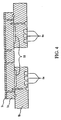
- the caps in FIGS. 3 and 4 include a distributed resistive heater attached to the upper surface of the electrode cap bottom 1b. These heaters may be placed in the electrode cap top 1a or in the electrode cap bottom 1b.
- the resistive heater may be a spirally wound cable heater 17 as shown in FIG. 3 , for example, or a thin annular strip or mica foil heater 18 as shown in FIG. 4 .
- the cable heater 17, for example a nichrome wire heater, is preferred because it allows a relatively large interface surface between the cap top 1a and cap bottom 1b resulting in improved thermal communication.
- the heater may be 1/16 inch in diameter and 65 inches long, with a stainless steel sheath, providing around 500 W at 120 V.
- the cable can be inserted in a spiral machined into the cap bottom 1b and pressed into place to yield a flush upper surface on the cap bottom 1b.
- the cable heater would be embedded within the mold of a cast cap bottom.
- the mica foil heaters 18 in FIG. 4 are composed of an etched foil encapsulated by mica insulation on all sides. These mica foil heaters are typically less than 1 mm thick and can easily provide as much as 100 W/in 2 when operating at 260°c. Alternatively, these mica heaters can be enclosed in a steel sheath (typically less than 5 mm thick) and provide up to 50 W/in 2 power densities. Other annular heaters could also be used, for example, boron nitride heaters.
- FIGS. 3 and 4 may additionally incorporate the other elements of the electrode cap described in reference to FIGS. 1 and 2 , such as cooling channels, temperature sensor, and the like. For simplicity, these additional features are not shown in FIGS. 3 and 4 .
- the lower electrode 2 in FIG. 1 when used with the electrode caps of FIGS. 3 or 4 , may not contain the resistive cartridge heaters 10.
- the active temperature control achieved through the use of feedback control described above in reference to FIG. 1 is used with the electrode cap of FIGS. 3 and 4 in the same manner, except that the heating voltage may be supplied to the cable or foil heating elements instead of, or in addition to, to the resistive cartridge heating elements 10.
Landscapes
- Engineering & Computer Science (AREA)
- Physics & Mathematics (AREA)
- Condensed Matter Physics & Semiconductors (AREA)
- General Physics & Mathematics (AREA)
- Manufacturing & Machinery (AREA)
- Computer Hardware Design (AREA)
- Microelectronics & Electronic Packaging (AREA)
- Power Engineering (AREA)
- Container, Conveyance, Adherence, Positioning, Of Wafer (AREA)
- Chemical Vapour Deposition (AREA)
- Crystals, And After-Treatments Of Crystals (AREA)
- Physical Vapour Deposition (AREA)
Claims (14)
- Elektrostatische Aufspannvorrichtung (100) zum elektrostatischen Anziehen und Halten eines Objekts (4) mit Vorder- und Rückseite, wobei die Vorrichtung aufweist:eine Elektrodenkappe (1) mit Ober- und Unterseite, die mit einer auf die Oberseite aufgebrachten dielektrischen Schicht (1c) versehen ist, wobei die Elektrodenkappe mit einer ersten Kanaleinrichtung (5a, 5b, 5c) und einer zweiten Kanaleinrichtung (6a) ausgestattet ist;eine untere Elektrode (2) mit Ober- und Unterseite, wobei die Oberseite der unteren Elektrode (2) an der Unterseite der Elektrodenkappe (1) befestigt ist, wobei die untere Elektrode (2) mit einer dritten Kanaleinrichtung (5) und einer vierten Kanaleinrichtung (6) ausgestattet ist, wobei die dritte Kanaleinrichtung (5) der unteren Elektrode (2) und die erste Kanaleinrichtung (5a, 5b, 5c) der Elektrodenkappe (1) einen Kanal zum Transport eines wärmeleitenden Gases von der Unterseite der unteren Elektrode zur Rückseite des Objekts (4) bilden, und wobei die zweite Kanaleinrichtung (6a) der Elektrodenkappe (1) und die vierte Kanaleinrichtung (6) der unteren Elektrode (2) einen Kanal zum Transport einer umlaufenden Kühlmittelflüssigkeit von der Unterseite der unteren Elektrode (2) zur Elektrodenkappe (1) bilden;in der unteren Elektrode montierte Heizeinrichtungen (10, 17, 18) zum Beheizen der elektrostatischen Aufspannvorrichtung (100), undeine Regelung mit Rückführung, um die Aufspannvorrichtung auf einer vorgegebenen Temperatur zu halten, wobei die Regelung mit Rückführung eine Einrichtung zur Regelung der Heizeinrichtungen (10, 17, 18) und eine Einrichtung zur Regelung der Kühhnittelflüssigkeitsumwälzeinrichtung einschließt.
- Elektrostatische Aufspannvorrichtung nach Anspruch 1, die ferner eine Gleichstromvorspanneinrichtung zum Vorspannen der elektrostatischen Aufspannvorrichtung, um eine elektrostatische Klemmspannung bereitzustellen, und eine DC-Vorspanneinrichtung zum Anlegen einer Vorspannungsleistung an das Objekt aufweist.
- Elektrostatische Aufspannvorrichtung nach Anspruch 1, wobei die Einrichtung zur Regelung der Heizeinrichtungen eine für die Heizeinrichtungen vorgesehene Stromversorgung mit veränderlicher Spannung enthält, wodurch der für die Heizeinrichtungen bereitgestellte Leistungsbetrag geregelt werden kann.
- Elektrostatische Aufspannvorrichtung nach Anspruch 1, wobei die Einrichtung zur Regelung der Flüssigkeitsumwälzeinrichtung einen Durchflußregler enthält, wodurch die Durchflußgeschwindigkeit der umlaufenden Flüssigkeit durch die Elektrodenkappe geregelt werden kann.
- Elektrostatische Aufspannvorrichtung nach Anspruch 1, wobei die Heizeinrichtung aus einer Vielzahl von zylinderförmigen Widerstands-Patronenheizkörpern (10) besteht.
- Elektrostatische Aufspannvorrichtung nach Anspruch 1, wobei die Heizeinrichtung ein Widerstands-Kabelheizkörper (17) ist.
- Elektrostatische Aufspannvorrichtung nach Anspruch 1, wobei die Heizeinrichtung ein ringförmiger Bandheizkörper (18) ist.
- Elektrostatische Aufspannvorrichtung nach Anspruch 1, wobei die Elektrodenkappe (I) aus Aluminium besteht und die Oberseite (1a) der Elektrodenkappe mit einer aus Aluminiumoxid bestehenden dielektrischen Schicht (1c) versehen ist.
- Elektrostatische Aufspannvorrichtung nach Anspruch 1, wobei die Elektrodenkappe (1) aus Molybdän besteht und die Oberseite (1a) der Elektrodenkappe mit einer aus Diamant bestehenden dielektrischen Schicht (1c) versehen ist.
- Elektrostatische Aufspannvorrichtung nach Anspruch 9, wobei die Dicke der dielektrischen Diamantschicht annähernd 5 - 50 µm beträgt.
- Elektrostatische Aufspannvorrichtung nach Anspruch 1, wobei die Elektrodenkappe (1) metallisch ist und die Oberseite (1a) der Elektrodenkappe mit einer aus Keramik bestehenden dielektrischen Schicht (1c) versehen ist.
- Elektrostatische Aufspannvornchtung nach Anspruch 11, wobei die Keramik Aluminiuinnitiid ist.
- Elektrostatische Aufspannvorrichtung nach Anspruch 1, wobei das wärmeleitende Gas Helium, Argon, Stickstoff oder Sauerstoff ist.
- Elektrostatische Aufspannvorrichtung nach Anspruch 1, wobei das umlaufende flüssige Kühlmittel entionisiertes Wasser, Ethylenglycol, Fluorinert, Siliconöl oder ein Gemisch aus entionisiertem Wasser und Ethylenglycol ist.
Applications Claiming Priority (3)
| Application Number | Priority Date | Filing Date | Title |
|---|---|---|---|
| US08/724,005 US5835334A (en) | 1996-09-30 | 1996-09-30 | Variable high temperature chuck for high density plasma chemical vapor deposition |
| US724005 | 1996-09-30 | ||
| PCT/US1997/017576 WO1998014999A1 (en) | 1996-09-30 | 1997-09-30 | Variable high temperature chuck for high density plasma chemical vapor deposition |
Publications (2)
| Publication Number | Publication Date |
|---|---|
| EP0938747A1 EP0938747A1 (de) | 1999-09-01 |
| EP0938747B1 true EP0938747B1 (de) | 2009-11-18 |
Family
ID=24908563
Family Applications (1)
| Application Number | Title | Priority Date | Filing Date |
|---|---|---|---|
| EP97943648A Expired - Lifetime EP0938747B1 (de) | 1996-09-30 | 1997-09-30 | Regulierbarer, hochtemperatur-halter für plasma-cvd einer hohen dichte |
Country Status (8)
| Country | Link |
|---|---|
| US (1) | US5835334A (de) |
| EP (1) | EP0938747B1 (de) |
| JP (1) | JP4149002B2 (de) |
| KR (1) | KR100372281B1 (de) |
| AT (1) | ATE449419T1 (de) |
| AU (1) | AU4507297A (de) |
| DE (1) | DE69739660D1 (de) |
| WO (1) | WO1998014999A1 (de) |
Cited By (1)
| Publication number | Priority date | Publication date | Assignee | Title |
|---|---|---|---|---|
| EP3555910B1 (de) * | 2016-12-16 | 2023-06-14 | Applied Materials, Inc. | Drehbares elektrostatisches futter mit rückseitiger gasversorgung |
Families Citing this family (176)
| Publication number | Priority date | Publication date | Assignee | Title |
|---|---|---|---|---|
| US6184158B1 (en) * | 1996-12-23 | 2001-02-06 | Lam Research Corporation | Inductively coupled plasma CVD |
| US5956609A (en) * | 1997-08-11 | 1999-09-21 | Taiwan Semiconductor Manufacturing Company, Ltd. | Method for reducing stress and improving step-coverage of tungsten interconnects and plugs |
| US6328096B1 (en) * | 1997-12-31 | 2001-12-11 | Temptronic Corporation | Workpiece chuck |
| US6359264B1 (en) * | 1998-03-11 | 2002-03-19 | Applied Materials, Inc. | Thermal cycling module |
| US6433314B1 (en) | 1998-04-08 | 2002-08-13 | Applied Materials, Inc. | Direct temperature control for a component of a substrate processing chamber |
| US6200911B1 (en) * | 1998-04-21 | 2001-03-13 | Applied Materials, Inc. | Method and apparatus for modifying the profile of narrow, high-aspect-ratio gaps using differential plasma power |
| JP3453069B2 (ja) * | 1998-08-20 | 2003-10-06 | 東京エレクトロン株式会社 | 基板温調装置 |
| DE69925291T2 (de) * | 1998-09-22 | 2005-10-06 | Ballard Power Systems Ag | Kühlsubsystem mit frostschutzmittel |
| JP3892609B2 (ja) | 1999-02-16 | 2007-03-14 | 株式会社東芝 | ホットプレートおよび半導体装置の製造方法 |
| US6169652B1 (en) | 1999-03-12 | 2001-01-02 | Euv, L.L.C. | Electrostatically screened, voltage-controlled electrostatic chuck |
| EP1193751B1 (de) * | 1999-04-06 | 2006-05-17 | Tokyo Electron Limited | Elektrode und herstellungsmethode für eine elektrode |
| US6395095B1 (en) * | 1999-06-15 | 2002-05-28 | Tokyo Electron Limited | Process apparatus and method for improved plasma processing of a substrate |
| US6367413B1 (en) | 1999-06-15 | 2002-04-09 | Tokyo Electron Limited | Apparatus for monitoring substrate biasing during plasma processing of a substrate |
| US6431112B1 (en) * | 1999-06-15 | 2002-08-13 | Tokyo Electron Limited | Apparatus and method for plasma processing of a substrate utilizing an electrostatic chuck |
| JP2001068538A (ja) * | 1999-06-21 | 2001-03-16 | Tokyo Electron Ltd | 電極構造、載置台構造、プラズマ処理装置及び処理装置 |
| KR100574924B1 (ko) * | 1999-08-18 | 2006-04-28 | 삼성전자주식회사 | 세라믹 링을 구비하는 정전척 및 그 제조방법 |
| US6278089B1 (en) * | 1999-11-02 | 2001-08-21 | Applied Materials, Inc. | Heater for use in substrate processing |
| US6377437B1 (en) | 1999-12-22 | 2002-04-23 | Lam Research Corporation | High temperature electrostatic chuck |
| JP3565496B2 (ja) * | 2000-04-13 | 2004-09-15 | イビデン株式会社 | セラミックヒータ、静電チャックおよびウエハプローバ |
| US6606234B1 (en) | 2000-09-05 | 2003-08-12 | Saint-Gobain Ceramics & Plastics, Inc. | Electrostatic chuck and method for forming an electrostatic chuck having porous regions for fluid flow |
| WO2002045871A1 (en) * | 2000-12-06 | 2002-06-13 | Angstron Systems, Inc. | System and method for modulated ion-induced atomic layer deposition (mii-ald) |
| JP4311600B2 (ja) * | 2001-01-30 | 2009-08-12 | 日本碍子株式会社 | 静電チャック用接合構造体及びその製造方法 |
| US20020144786A1 (en) * | 2001-04-05 | 2002-10-10 | Angstron Systems, Inc. | Substrate temperature control in an ALD reactor |
| EP1254606A1 (de) * | 2001-05-04 | 2002-11-06 | Philip Morris Products S.A. | Einrichtung und Verfahren zum Lösen von Tabakballen |
| KR100397047B1 (ko) * | 2001-05-08 | 2003-09-02 | 삼성전자주식회사 | 정전척의 냉각장치 및 방법 |
| JP4720019B2 (ja) * | 2001-05-18 | 2011-07-13 | 東京エレクトロン株式会社 | 冷却機構及び処理装置 |
| US6577113B2 (en) | 2001-06-06 | 2003-06-10 | Tokyo Electron Limited | Apparatus and method for measuring substrate biasing during plasma processing of a substrate |
| US6669783B2 (en) | 2001-06-28 | 2003-12-30 | Lam Research Corporation | High temperature electrostatic chuck |
| TWI246873B (en) | 2001-07-10 | 2006-01-01 | Tokyo Electron Ltd | Plasma processing device |
| JP2003060019A (ja) * | 2001-08-13 | 2003-02-28 | Hitachi Ltd | ウエハステージ |
| DE10156407A1 (de) * | 2001-11-16 | 2003-06-05 | Bosch Gmbh Robert | Haltevorrichtung, insbesondere zum Fixieren eines Halbleiterwafers in einer Plasmaätzvorrichtung, und Verfahren zur Wärmezufuhr oder Wärmeabfuhr von einem Substrat |
| TW561515B (en) * | 2001-11-30 | 2003-11-11 | Tokyo Electron Ltd | Processing device, and gas discharge suppressing member |
| KR20030047341A (ko) * | 2001-12-10 | 2003-06-18 | 삼성전자주식회사 | 이온주입장치의 정전척 |
| US6632325B2 (en) * | 2002-02-07 | 2003-10-14 | Applied Materials, Inc. | Article for use in a semiconductor processing chamber and method of fabricating same |
| US6677167B2 (en) * | 2002-03-04 | 2004-01-13 | Hitachi High-Technologies Corporation | Wafer processing apparatus and a wafer stage and a wafer processing method |
| US6646233B2 (en) * | 2002-03-05 | 2003-11-11 | Hitachi High-Technologies Corporation | Wafer stage for wafer processing apparatus and wafer processing method |
| DE10216786C5 (de) * | 2002-04-15 | 2009-10-15 | Ers Electronic Gmbh | Verfahren und Vorrichtung zur Konditionierung von Halbleiterwafern und/oder Hybriden |
| KR100456093B1 (ko) * | 2002-04-19 | 2004-11-08 | 국방과학연구소 | 열류 게이지 및 그 제조방법 |
| KR100457833B1 (ko) * | 2002-05-24 | 2004-11-18 | 주성엔지니어링(주) | 플라즈마 식각 장치 |
| US7156951B1 (en) * | 2002-06-21 | 2007-01-02 | Lam Research Corporation | Multiple zone gas distribution apparatus for thermal control of semiconductor wafer |
| US20040052969A1 (en) * | 2002-09-16 | 2004-03-18 | Applied Materials, Inc. | Methods for operating a chemical vapor deposition chamber using a heated gas distribution plate |
| US6946033B2 (en) * | 2002-09-16 | 2005-09-20 | Applied Materials Inc. | Heated gas distribution plate for a processing chamber |
| US7347901B2 (en) * | 2002-11-29 | 2008-03-25 | Tokyo Electron Limited | Thermally zoned substrate holder assembly |
| US7033443B2 (en) * | 2003-03-28 | 2006-04-25 | Axcelis Technologies, Inc. | Gas-cooled clamp for RTP |
| US20040187787A1 (en) | 2003-03-31 | 2004-09-30 | Dawson Keith E. | Substrate support having temperature controlled substrate support surface |
| US7993460B2 (en) * | 2003-06-30 | 2011-08-09 | Lam Research Corporation | Substrate support having dynamic temperature control |
| EP1530088B1 (de) * | 2003-11-05 | 2007-08-08 | ASML Netherlands B.V. | Lithographischer Apparat |
| KR100508754B1 (ko) * | 2003-12-22 | 2005-08-17 | 삼성전자주식회사 | 온도 컨트롤러 및 이를 갖는 식각 장치 |
| DE102004024649B4 (de) * | 2004-05-18 | 2007-02-01 | Thallner, Erich, Dipl.-Ing. | Justiereinrichtung und Vorrichtung zum Justieren eines Wafers |
| US7731798B2 (en) * | 2004-12-01 | 2010-06-08 | Ultratech, Inc. | Heated chuck for laser thermal processing |
| JP4694249B2 (ja) * | 2005-04-20 | 2011-06-08 | 株式会社日立ハイテクノロジーズ | 真空処理装置及び試料の真空処理方法 |
| JP5004436B2 (ja) * | 2005-05-23 | 2012-08-22 | 東京エレクトロン株式会社 | 静電吸着電極および処理装置 |
| US20070283891A1 (en) * | 2006-03-29 | 2007-12-13 | Nobuyuki Okayama | Table for supporting substrate, and vacuum-processing equipment |
| US8226769B2 (en) * | 2006-04-27 | 2012-07-24 | Applied Materials, Inc. | Substrate support with electrostatic chuck having dual temperature zones |
| KR100798813B1 (ko) * | 2006-07-25 | 2008-01-28 | 삼성전자주식회사 | 정전척 어셈블리 및 정전척 온도 제어방법 |
| US8491752B2 (en) * | 2006-12-15 | 2013-07-23 | Tokyo Electron Limited | Substrate mounting table and method for manufacturing same, substrate processing apparatus, and fluid supply mechanism |
| JP4937724B2 (ja) * | 2006-12-15 | 2012-05-23 | 東京エレクトロン株式会社 | 基板載置台、基板載置台の製造方法、基板処理装置、流体供給機構 |
| JP4450106B1 (ja) * | 2008-03-11 | 2010-04-14 | 東京エレクトロン株式会社 | 載置台構造及び処理装置 |
| US8900404B2 (en) * | 2008-06-10 | 2014-12-02 | Lam Research Corporation | Plasma processing systems with mechanisms for controlling temperatures of components |
| US9543181B2 (en) * | 2008-07-30 | 2017-01-10 | Taiwan Semiconductor Manufacturing Company, Ltd. | Replaceable electrostatic chuck sidewall shield |
| US10297550B2 (en) | 2010-02-05 | 2019-05-21 | Taiwan Semiconductor Manufacturing Company, Ltd. | 3D IC architecture with interposer and interconnect structure for bonding dies |
| US9324576B2 (en) | 2010-05-27 | 2016-04-26 | Applied Materials, Inc. | Selective etch for silicon films |
| US10283321B2 (en) | 2011-01-18 | 2019-05-07 | Applied Materials, Inc. | Semiconductor processing system and methods using capacitively coupled plasma |
| US9064815B2 (en) | 2011-03-14 | 2015-06-23 | Applied Materials, Inc. | Methods for etch of metal and metal-oxide films |
| US8999856B2 (en) | 2011-03-14 | 2015-04-07 | Applied Materials, Inc. | Methods for etch of sin films |
| KR101872886B1 (ko) | 2011-03-17 | 2018-06-29 | 에이에스엠엘 네델란즈 비.브이. | 정전기 클램프, 리소그래피 장치, 및 디바이스 제조 방법 |
| NL2008630A (en) | 2011-04-27 | 2012-10-30 | Asml Netherlands Bv | Substrate holder, lithographic apparatus, device manufacturing method, and method of manufacturing a substrate holder. |
| US9673037B2 (en) * | 2011-05-31 | 2017-06-06 | Law Research Corporation | Substrate freeze dry apparatus and method |
| JP6223983B2 (ja) * | 2011-09-30 | 2017-11-01 | アプライド マテリアルズ インコーポレイテッドApplied Materials,Incorporated | 温度制御付き静電チャック |
| US9494875B2 (en) | 2011-10-06 | 2016-11-15 | Asml Netherlands B.V. | Chuck, a chuck control system, a lithography apparatus and a method of using a chuck |
| US10256123B2 (en) | 2011-10-27 | 2019-04-09 | Applied Materials, Inc. | Component temperature control using a combination of proportional control valves and pulsed valves |
| US9267739B2 (en) | 2012-07-18 | 2016-02-23 | Applied Materials, Inc. | Pedestal with multi-zone temperature control and multiple purge capabilities |
| US9373517B2 (en) | 2012-08-02 | 2016-06-21 | Applied Materials, Inc. | Semiconductor processing with DC assisted RF power for improved control |
| US9132436B2 (en) | 2012-09-21 | 2015-09-15 | Applied Materials, Inc. | Chemical control features in wafer process equipment |
| US8898928B2 (en) * | 2012-10-11 | 2014-12-02 | Lam Research Corporation | Delamination drying apparatus and method |
| US10256079B2 (en) | 2013-02-08 | 2019-04-09 | Applied Materials, Inc. | Semiconductor processing systems having multiple plasma configurations |
| US9362130B2 (en) | 2013-03-01 | 2016-06-07 | Applied Materials, Inc. | Enhanced etching processes using remote plasma sources |
| US9773648B2 (en) | 2013-08-30 | 2017-09-26 | Applied Materials, Inc. | Dual discharge modes operation for remote plasma |
| US9520303B2 (en) | 2013-11-12 | 2016-12-13 | Applied Materials, Inc. | Aluminum selective etch |
| US9496157B2 (en) * | 2013-11-14 | 2016-11-15 | Taiwan Semiconductor Manufacturing Co., Ltd. | Ultraviolet curing apparatus having top liner and bottom liner made of low-coefficient of thermal expansion material |
| US9622375B2 (en) | 2013-12-31 | 2017-04-11 | Applied Materials, Inc. | Electrostatic chuck with external flow adjustments for improved temperature distribution |
| US9299537B2 (en) | 2014-03-20 | 2016-03-29 | Applied Materials, Inc. | Radial waveguide systems and methods for post-match control of microwaves |
| US9903020B2 (en) | 2014-03-31 | 2018-02-27 | Applied Materials, Inc. | Generation of compact alumina passivation layers on aluminum plasma equipment components |
| US9309598B2 (en) | 2014-05-28 | 2016-04-12 | Applied Materials, Inc. | Oxide and metal removal |
| US9496167B2 (en) | 2014-07-31 | 2016-11-15 | Applied Materials, Inc. | Integrated bit-line airgap formation and gate stack post clean |
| US9659753B2 (en) | 2014-08-07 | 2017-05-23 | Applied Materials, Inc. | Grooved insulator to reduce leakage current |
| WO2016025573A1 (en) * | 2014-08-15 | 2016-02-18 | Applied Materials, Inc. | Method and apparatus of processing wafers with compressive or tensile stress at elevated temperatures in a plasma enhanced chemical vapor deposition system |
| US9613822B2 (en) | 2014-09-25 | 2017-04-04 | Applied Materials, Inc. | Oxide etch selectivity enhancement |
| US9960060B2 (en) * | 2014-10-10 | 2018-05-01 | Varian Semiconductor Equipment Associates, Inc. | Platen assembly |
| US9355922B2 (en) | 2014-10-14 | 2016-05-31 | Applied Materials, Inc. | Systems and methods for internal surface conditioning in plasma processing equipment |
| US9966240B2 (en) | 2014-10-14 | 2018-05-08 | Applied Materials, Inc. | Systems and methods for internal surface conditioning assessment in plasma processing equipment |
| US11637002B2 (en) | 2014-11-26 | 2023-04-25 | Applied Materials, Inc. | Methods and systems to enhance process uniformity |
| US10573496B2 (en) | 2014-12-09 | 2020-02-25 | Applied Materials, Inc. | Direct outlet toroidal plasma source |
| US10224210B2 (en) | 2014-12-09 | 2019-03-05 | Applied Materials, Inc. | Plasma processing system with direct outlet toroidal plasma source |
| US11257693B2 (en) | 2015-01-09 | 2022-02-22 | Applied Materials, Inc. | Methods and systems to improve pedestal temperature control |
| US9728437B2 (en) | 2015-02-03 | 2017-08-08 | Applied Materials, Inc. | High temperature chuck for plasma processing systems |
| US20160225652A1 (en) | 2015-02-03 | 2016-08-04 | Applied Materials, Inc. | Low temperature chuck for plasma processing systems |
| US9881805B2 (en) | 2015-03-02 | 2018-01-30 | Applied Materials, Inc. | Silicon selective removal |
| US10288361B2 (en) * | 2015-03-17 | 2019-05-14 | Hatco Corporation | Hot and cold shelf assembly with replaceable heating elements |
| TWI703671B (zh) * | 2015-08-06 | 2020-09-01 | 美商應用材料股份有限公司 | 螺接式晶圓夾具熱管理系統及用於晶圓處理系統的方法 |
| US9691645B2 (en) | 2015-08-06 | 2017-06-27 | Applied Materials, Inc. | Bolted wafer chuck thermal management systems and methods for wafer processing systems |
| US9741593B2 (en) | 2015-08-06 | 2017-08-22 | Applied Materials, Inc. | Thermal management systems and methods for wafer processing systems |
| US9349605B1 (en) | 2015-08-07 | 2016-05-24 | Applied Materials, Inc. | Oxide etch selectivity systems and methods |
| US10504700B2 (en) | 2015-08-27 | 2019-12-10 | Applied Materials, Inc. | Plasma etching systems and methods with secondary plasma injection |
| US9805963B2 (en) * | 2015-10-05 | 2017-10-31 | Lam Research Corporation | Electrostatic chuck with thermal choke |
| US10522371B2 (en) | 2016-05-19 | 2019-12-31 | Applied Materials, Inc. | Systems and methods for improved semiconductor etching and component protection |
| US10504754B2 (en) | 2016-05-19 | 2019-12-10 | Applied Materials, Inc. | Systems and methods for improved semiconductor etching and component protection |
| US9865484B1 (en) | 2016-06-29 | 2018-01-09 | Applied Materials, Inc. | Selective etch using material modification and RF pulsing |
| US10062575B2 (en) | 2016-09-09 | 2018-08-28 | Applied Materials, Inc. | Poly directional etch by oxidation |
| US10629473B2 (en) | 2016-09-09 | 2020-04-21 | Applied Materials, Inc. | Footing removal for nitride spacer |
| US10546729B2 (en) | 2016-10-04 | 2020-01-28 | Applied Materials, Inc. | Dual-channel showerhead with improved profile |
| US10062585B2 (en) | 2016-10-04 | 2018-08-28 | Applied Materials, Inc. | Oxygen compatible plasma source |
| US9721789B1 (en) | 2016-10-04 | 2017-08-01 | Applied Materials, Inc. | Saving ion-damaged spacers |
| US9934942B1 (en) | 2016-10-04 | 2018-04-03 | Applied Materials, Inc. | Chamber with flow-through source |
| US10062579B2 (en) | 2016-10-07 | 2018-08-28 | Applied Materials, Inc. | Selective SiN lateral recess |
| US9947549B1 (en) | 2016-10-10 | 2018-04-17 | Applied Materials, Inc. | Cobalt-containing material removal |
| US10163696B2 (en) | 2016-11-11 | 2018-12-25 | Applied Materials, Inc. | Selective cobalt removal for bottom up gapfill |
| US9768034B1 (en) | 2016-11-11 | 2017-09-19 | Applied Materials, Inc. | Removal methods for high aspect ratio structures |
| US10026621B2 (en) | 2016-11-14 | 2018-07-17 | Applied Materials, Inc. | SiN spacer profile patterning |
| US10242908B2 (en) | 2016-11-14 | 2019-03-26 | Applied Materials, Inc. | Airgap formation with damage-free copper |
| US10566206B2 (en) | 2016-12-27 | 2020-02-18 | Applied Materials, Inc. | Systems and methods for anisotropic material breakthrough |
| CN206432233U (zh) * | 2017-01-19 | 2017-08-22 | 江苏鲁汶仪器有限公司 | 刻蚀机的下电极载片台 |
| US10431429B2 (en) | 2017-02-03 | 2019-10-01 | Applied Materials, Inc. | Systems and methods for radial and azimuthal control of plasma uniformity |
| US10403507B2 (en) | 2017-02-03 | 2019-09-03 | Applied Materials, Inc. | Shaped etch profile with oxidation |
| US10043684B1 (en) | 2017-02-06 | 2018-08-07 | Applied Materials, Inc. | Self-limiting atomic thermal etching systems and methods |
| US10319739B2 (en) | 2017-02-08 | 2019-06-11 | Applied Materials, Inc. | Accommodating imperfectly aligned memory holes |
| US10943834B2 (en) | 2017-03-13 | 2021-03-09 | Applied Materials, Inc. | Replacement contact process |
| US10319649B2 (en) | 2017-04-11 | 2019-06-11 | Applied Materials, Inc. | Optical emission spectroscopy (OES) for remote plasma monitoring |
| US11276559B2 (en) | 2017-05-17 | 2022-03-15 | Applied Materials, Inc. | Semiconductor processing chamber for multiple precursor flow |
| US11276590B2 (en) | 2017-05-17 | 2022-03-15 | Applied Materials, Inc. | Multi-zone semiconductor substrate supports |
| JP7176860B6 (ja) | 2017-05-17 | 2022-12-16 | アプライド マテリアルズ インコーポレイテッド | 前駆体の流れを改善する半導体処理チャンバ |
| US10049891B1 (en) | 2017-05-31 | 2018-08-14 | Applied Materials, Inc. | Selective in situ cobalt residue removal |
| US10497579B2 (en) | 2017-05-31 | 2019-12-03 | Applied Materials, Inc. | Water-free etching methods |
| US10920320B2 (en) | 2017-06-16 | 2021-02-16 | Applied Materials, Inc. | Plasma health determination in semiconductor substrate processing reactors |
| EP3642869A1 (de) * | 2017-06-23 | 2020-04-29 | Watlow Electric Manufacturing Company | Sockel für hochtemperatur-heizplatte |
| US10541246B2 (en) | 2017-06-26 | 2020-01-21 | Applied Materials, Inc. | 3D flash memory cells which discourage cross-cell electrical tunneling |
| US10727080B2 (en) | 2017-07-07 | 2020-07-28 | Applied Materials, Inc. | Tantalum-containing material removal |
| US10541184B2 (en) | 2017-07-11 | 2020-01-21 | Applied Materials, Inc. | Optical emission spectroscopic techniques for monitoring etching |
| US10354889B2 (en) | 2017-07-17 | 2019-07-16 | Applied Materials, Inc. | Non-halogen etching of silicon-containing materials |
| US10043674B1 (en) | 2017-08-04 | 2018-08-07 | Applied Materials, Inc. | Germanium etching systems and methods |
| US10170336B1 (en) | 2017-08-04 | 2019-01-01 | Applied Materials, Inc. | Methods for anisotropic control of selective silicon removal |
| US10297458B2 (en) | 2017-08-07 | 2019-05-21 | Applied Materials, Inc. | Process window widening using coated parts in plasma etch processes |
| US10283324B1 (en) | 2017-10-24 | 2019-05-07 | Applied Materials, Inc. | Oxygen treatment for nitride etching |
| US10128086B1 (en) | 2017-10-24 | 2018-11-13 | Applied Materials, Inc. | Silicon pretreatment for nitride removal |
| US10256112B1 (en) | 2017-12-08 | 2019-04-09 | Applied Materials, Inc. | Selective tungsten removal |
| US10903054B2 (en) | 2017-12-19 | 2021-01-26 | Applied Materials, Inc. | Multi-zone gas distribution systems and methods |
| US11328909B2 (en) | 2017-12-22 | 2022-05-10 | Applied Materials, Inc. | Chamber conditioning and removal processes |
| US10854426B2 (en) | 2018-01-08 | 2020-12-01 | Applied Materials, Inc. | Metal recess for semiconductor structures |
| US10964512B2 (en) | 2018-02-15 | 2021-03-30 | Applied Materials, Inc. | Semiconductor processing chamber multistage mixing apparatus and methods |
| US10679870B2 (en) | 2018-02-15 | 2020-06-09 | Applied Materials, Inc. | Semiconductor processing chamber multistage mixing apparatus |
| TWI716818B (zh) | 2018-02-28 | 2021-01-21 | 美商應用材料股份有限公司 | 形成氣隙的系統及方法 |
| US10593560B2 (en) | 2018-03-01 | 2020-03-17 | Applied Materials, Inc. | Magnetic induction plasma source for semiconductor processes and equipment |
| US10319600B1 (en) | 2018-03-12 | 2019-06-11 | Applied Materials, Inc. | Thermal silicon etch |
| US10497573B2 (en) | 2018-03-13 | 2019-12-03 | Applied Materials, Inc. | Selective atomic layer etching of semiconductor materials |
| CN111989770B (zh) * | 2018-03-23 | 2024-07-16 | 应用材料公司 | 隔离的背侧氦输送系统 |
| US10573527B2 (en) | 2018-04-06 | 2020-02-25 | Applied Materials, Inc. | Gas-phase selective etching systems and methods |
| US10490406B2 (en) | 2018-04-10 | 2019-11-26 | Appled Materials, Inc. | Systems and methods for material breakthrough |
| US10699879B2 (en) | 2018-04-17 | 2020-06-30 | Applied Materials, Inc. | Two piece electrode assembly with gap for plasma control |
| US10886137B2 (en) | 2018-04-30 | 2021-01-05 | Applied Materials, Inc. | Selective nitride removal |
| US10872778B2 (en) | 2018-07-06 | 2020-12-22 | Applied Materials, Inc. | Systems and methods utilizing solid-phase etchants |
| US10755941B2 (en) | 2018-07-06 | 2020-08-25 | Applied Materials, Inc. | Self-limiting selective etching systems and methods |
| US10672642B2 (en) | 2018-07-24 | 2020-06-02 | Applied Materials, Inc. | Systems and methods for pedestal configuration |
| US11049755B2 (en) | 2018-09-14 | 2021-06-29 | Applied Materials, Inc. | Semiconductor substrate supports with embedded RF shield |
| US10892198B2 (en) | 2018-09-14 | 2021-01-12 | Applied Materials, Inc. | Systems and methods for improved performance in semiconductor processing |
| US11062887B2 (en) | 2018-09-17 | 2021-07-13 | Applied Materials, Inc. | High temperature RF heater pedestals |
| US11417534B2 (en) | 2018-09-21 | 2022-08-16 | Applied Materials, Inc. | Selective material removal |
| JP7152926B2 (ja) * | 2018-10-05 | 2022-10-13 | 日本特殊陶業株式会社 | 保持装置 |
| US11682560B2 (en) | 2018-10-11 | 2023-06-20 | Applied Materials, Inc. | Systems and methods for hafnium-containing film removal |
| US11121002B2 (en) | 2018-10-24 | 2021-09-14 | Applied Materials, Inc. | Systems and methods for etching metals and metal derivatives |
| US11437242B2 (en) | 2018-11-27 | 2022-09-06 | Applied Materials, Inc. | Selective removal of silicon-containing materials |
| US11721527B2 (en) | 2019-01-07 | 2023-08-08 | Applied Materials, Inc. | Processing chamber mixing systems |
| US10920319B2 (en) | 2019-01-11 | 2021-02-16 | Applied Materials, Inc. | Ceramic showerheads with conductive electrodes |
| CN113728424A (zh) * | 2019-04-22 | 2021-11-30 | 朗姆研究公司 | 具有对于晶片的空间性可调谐rf耦合的静电卡盘 |
| JP7301021B2 (ja) * | 2020-05-01 | 2023-06-30 | 東京エレクトロン株式会社 | 基板処理装置、載置台及び温度制御方法 |
| JP7575175B2 (ja) * | 2020-12-22 | 2024-10-29 | 東京エレクトロン株式会社 | 基板処理装置、基板処理装置の温度制御方法及び基板処理装置を制御する制御装置のプログラム |
| JP2025176267A (ja) * | 2024-05-21 | 2025-12-04 | Toto株式会社 | 静電チャック |
Citations (1)
| Publication number | Priority date | Publication date | Assignee | Title |
|---|---|---|---|---|
| JPH0813027A (ja) * | 1994-06-24 | 1996-01-16 | Mitsubishi Electric Corp | 誘導加熱装置 |
Family Cites Families (28)
| Publication number | Priority date | Publication date | Assignee | Title |
|---|---|---|---|---|
| US4384918A (en) * | 1980-09-30 | 1983-05-24 | Fujitsu Limited | Method and apparatus for dry etching and electrostatic chucking device used therein |
| JPS6372877A (ja) * | 1986-09-12 | 1988-04-02 | Tokuda Seisakusho Ltd | 真空処理装置 |
| JPH01152639A (ja) * | 1987-12-10 | 1989-06-15 | Canon Inc | 吸着保持装置 |
| US5111032A (en) * | 1989-03-13 | 1992-05-05 | Raychem Corporation | Method of making an electrical device comprising a conductive polymer |
| US5078851A (en) * | 1989-07-26 | 1992-01-07 | Kouji Nishihata | Low-temperature plasma processor |
| JP2737010B2 (ja) * | 1989-08-01 | 1998-04-08 | キヤノン株式会社 | 露光装置 |
| US4980566A (en) * | 1989-08-02 | 1990-12-25 | The United States Of America As Represented By The Secretary Of Commerce | Ultrashort pulse multichannel infrared spectrometer apparatus and method for obtaining ultrafast time resolution spectral data |
| US5221403A (en) * | 1990-07-20 | 1993-06-22 | Tokyo Electron Limited | Support table for plate-like body and processing apparatus using the table |
| US5055964A (en) * | 1990-09-07 | 1991-10-08 | International Business Machines Corporation | Electrostatic chuck having tapered electrodes |
| JPH04196528A (ja) * | 1990-11-28 | 1992-07-16 | Toshiba Corp | マグネトロンエッチング装置 |
| EP0493089B1 (de) * | 1990-12-25 | 1998-09-16 | Ngk Insulators, Ltd. | Heizungsapparat für eine Halbleiterscheibe und Verfahren zum Herstellen desselben |
| US5166856A (en) * | 1991-01-31 | 1992-11-24 | International Business Machines Corporation | Electrostatic chuck with diamond coating |
| US5155652A (en) * | 1991-05-02 | 1992-10-13 | International Business Machines Corporation | Temperature cycling ceramic electrostatic chuck |
| US5477975A (en) * | 1993-10-15 | 1995-12-26 | Applied Materials Inc | Plasma etch apparatus with heated scavenging surfaces |
| JP2752807B2 (ja) * | 1991-07-17 | 1998-05-18 | 株式会社日立製作所 | プラズマ処理装置 |
| US5376213A (en) * | 1992-07-28 | 1994-12-27 | Tokyo Electron Limited | Plasma processing apparatus |
| US5567267A (en) * | 1992-11-20 | 1996-10-22 | Tokyo Electron Limited | Method of controlling temperature of susceptor |
| US5413360A (en) * | 1992-12-01 | 1995-05-09 | Kyocera Corporation | Electrostatic chuck |
| KR100238629B1 (ko) * | 1992-12-17 | 2000-01-15 | 히가시 데쓰로 | 정전척을 가지는 재치대 및 이것을 이용한 플라즈마 처리장치 |
| US5436790A (en) * | 1993-01-15 | 1995-07-25 | Eaton Corporation | Wafer sensing and clamping monitor |
| KR100290748B1 (ko) * | 1993-01-29 | 2001-06-01 | 히가시 데쓰로 | 플라즈마 처리장치 |
| KR100260587B1 (ko) * | 1993-06-01 | 2000-08-01 | 히가시 데쓰로 | 정전척 및 그의 제조방법 |
| US5591269A (en) * | 1993-06-24 | 1997-01-07 | Tokyo Electron Limited | Vacuum processing apparatus |
| TW262566B (de) * | 1993-07-02 | 1995-11-11 | Tokyo Electron Co Ltd | |
| JP2647799B2 (ja) * | 1994-02-04 | 1997-08-27 | 日本碍子株式会社 | セラミックスヒーター及びその製造方法 |
| US5581874A (en) * | 1994-03-28 | 1996-12-10 | Tokyo Electron Limited | Method of forming a bonding portion |
| JPH07302785A (ja) * | 1994-05-09 | 1995-11-14 | Fujitsu Ltd | 基板処理装置及び基板温度制御方法 |
| US5609720A (en) * | 1995-09-29 | 1997-03-11 | Lam Research Corporation | Thermal control of semiconductor wafer during reactive ion etching |
-
1996
- 1996-09-30 US US08/724,005 patent/US5835334A/en not_active Expired - Lifetime
-
1997
- 1997-09-30 KR KR10-1999-7002736A patent/KR100372281B1/ko not_active Expired - Lifetime
- 1997-09-30 AT AT97943648T patent/ATE449419T1/de not_active IP Right Cessation
- 1997-09-30 JP JP51678898A patent/JP4149002B2/ja not_active Expired - Fee Related
- 1997-09-30 DE DE69739660T patent/DE69739660D1/de not_active Expired - Lifetime
- 1997-09-30 EP EP97943648A patent/EP0938747B1/de not_active Expired - Lifetime
- 1997-09-30 AU AU45072/97A patent/AU4507297A/en not_active Abandoned
- 1997-09-30 WO PCT/US1997/017576 patent/WO1998014999A1/en not_active Ceased
Patent Citations (1)
| Publication number | Priority date | Publication date | Assignee | Title |
|---|---|---|---|---|
| JPH0813027A (ja) * | 1994-06-24 | 1996-01-16 | Mitsubishi Electric Corp | 誘導加熱装置 |
Non-Patent Citations (1)
| Title |
|---|
| JOURNAL ARTICLE: "ELECTROSTATIC WAFER HOLDER FOR WAFER COOLING DURING REACTIVE ION ETCHING", IBM TECHNICAL DISCLOSURE BULLETIN, vol. 31, no. 1, 1 June 1988 (1988-06-01), IBM CORP. NEW YORK, US, pages 462 - 464, XP000119644 * |
Cited By (1)
| Publication number | Priority date | Publication date | Assignee | Title |
|---|---|---|---|---|
| EP3555910B1 (de) * | 2016-12-16 | 2023-06-14 | Applied Materials, Inc. | Drehbares elektrostatisches futter mit rückseitiger gasversorgung |
Also Published As
| Publication number | Publication date |
|---|---|
| JP2001502116A (ja) | 2001-02-13 |
| EP0938747A1 (de) | 1999-09-01 |
| AU4507297A (en) | 1998-04-24 |
| WO1998014999A1 (en) | 1998-04-09 |
| JP4149002B2 (ja) | 2008-09-10 |
| ATE449419T1 (de) | 2009-12-15 |
| KR20000048751A (ko) | 2000-07-25 |
| KR100372281B1 (ko) | 2003-02-19 |
| US5835334A (en) | 1998-11-10 |
| DE69739660D1 (de) | 2009-12-31 |
Similar Documents
| Publication | Publication Date | Title |
|---|---|---|
| EP0938747B1 (de) | Regulierbarer, hochtemperatur-halter für plasma-cvd einer hohen dichte | |
| JP7242823B2 (ja) | 高温処理用静電チャックアセンブリ | |
| US11527429B2 (en) | Substrate support assembly for high temperature processes | |
| US5810933A (en) | Wafer cooling device | |
| US7667944B2 (en) | Polyceramic e-chuck | |
| US5155652A (en) | Temperature cycling ceramic electrostatic chuck | |
| US6490145B1 (en) | Substrate support pedestal | |
| JP3982854B2 (ja) | 流量レギュレータをもった静電チャック | |
| US8536494B2 (en) | Method and apparatus for controlling the spatial temperature distribution across the surface of a workpiece support | |
| US6022418A (en) | Vacuum processing method | |
| JP4256503B2 (ja) | 真空処理装置 | |
| US20250349590A1 (en) | Fabrication of substrate support devices using inorganic dielectric bonding | |
| US12185433B2 (en) | High-temperature substrate support assembly with failure protection | |
| CN121195340A (zh) | 使用无机介电键合的基板支撑装置的制造 |
Legal Events
| Date | Code | Title | Description |
|---|---|---|---|
| PUAI | Public reference made under article 153(3) epc to a published international application that has entered the european phase |
Free format text: ORIGINAL CODE: 0009012 |
|
| 17P | Request for examination filed |
Effective date: 19990412 |
|
| AK | Designated contracting states |
Kind code of ref document: A1 Designated state(s): AT BE CH DE DK ES FI FR GB GR IE IT LI LU MC NL PT SE |
|
| 17Q | First examination report despatched |
Effective date: 20030430 |
|
| GRAP | Despatch of communication of intention to grant a patent |
Free format text: ORIGINAL CODE: EPIDOSNIGR1 |
|
| GRAS | Grant fee paid |
Free format text: ORIGINAL CODE: EPIDOSNIGR3 |
|
| GRAA | (expected) grant |
Free format text: ORIGINAL CODE: 0009210 |
|
| AK | Designated contracting states |
Kind code of ref document: B1 Designated state(s): AT BE CH DE DK ES FI FR GB GR IE IT LI LU MC NL PT SE |
|
| REG | Reference to a national code |
Ref country code: GB Ref legal event code: FG4D |
|
| REG | Reference to a national code |
Ref country code: CH Ref legal event code: EP |
|
| REG | Reference to a national code |
Ref country code: IE Ref legal event code: FG4D |
|
| REF | Corresponds to: |
Ref document number: 69739660 Country of ref document: DE Date of ref document: 20091231 Kind code of ref document: P |
|
| REG | Reference to a national code |
Ref country code: NL Ref legal event code: VDEP Effective date: 20091118 |
|
| PG25 | Lapsed in a contracting state [announced via postgrant information from national office to epo] |
Ref country code: SE Free format text: LAPSE BECAUSE OF FAILURE TO SUBMIT A TRANSLATION OF THE DESCRIPTION OR TO PAY THE FEE WITHIN THE PRESCRIBED TIME-LIMIT Effective date: 20091118 Ref country code: PT Free format text: LAPSE BECAUSE OF FAILURE TO SUBMIT A TRANSLATION OF THE DESCRIPTION OR TO PAY THE FEE WITHIN THE PRESCRIBED TIME-LIMIT Effective date: 20100318 Ref country code: FI Free format text: LAPSE BECAUSE OF FAILURE TO SUBMIT A TRANSLATION OF THE DESCRIPTION OR TO PAY THE FEE WITHIN THE PRESCRIBED TIME-LIMIT Effective date: 20091118 Ref country code: ES Free format text: LAPSE BECAUSE OF FAILURE TO SUBMIT A TRANSLATION OF THE DESCRIPTION OR TO PAY THE FEE WITHIN THE PRESCRIBED TIME-LIMIT Effective date: 20100228 |
|
| PG25 | Lapsed in a contracting state [announced via postgrant information from national office to epo] |
Ref country code: BE Free format text: LAPSE BECAUSE OF FAILURE TO SUBMIT A TRANSLATION OF THE DESCRIPTION OR TO PAY THE FEE WITHIN THE PRESCRIBED TIME-LIMIT Effective date: 20091118 Ref country code: AT Free format text: LAPSE BECAUSE OF FAILURE TO SUBMIT A TRANSLATION OF THE DESCRIPTION OR TO PAY THE FEE WITHIN THE PRESCRIBED TIME-LIMIT Effective date: 20091118 |
|
| PG25 | Lapsed in a contracting state [announced via postgrant information from national office to epo] |
Ref country code: NL Free format text: LAPSE BECAUSE OF FAILURE TO SUBMIT A TRANSLATION OF THE DESCRIPTION OR TO PAY THE FEE WITHIN THE PRESCRIBED TIME-LIMIT Effective date: 20091118 Ref country code: DK Free format text: LAPSE BECAUSE OF FAILURE TO SUBMIT A TRANSLATION OF THE DESCRIPTION OR TO PAY THE FEE WITHIN THE PRESCRIBED TIME-LIMIT Effective date: 20091118 |
|
| PLBE | No opposition filed within time limit |
Free format text: ORIGINAL CODE: 0009261 |
|
| STAA | Information on the status of an ep patent application or granted ep patent |
Free format text: STATUS: NO OPPOSITION FILED WITHIN TIME LIMIT |
|
| 26N | No opposition filed |
Effective date: 20100819 |
|
| PG25 | Lapsed in a contracting state [announced via postgrant information from national office to epo] |
Ref country code: GR Free format text: LAPSE BECAUSE OF FAILURE TO SUBMIT A TRANSLATION OF THE DESCRIPTION OR TO PAY THE FEE WITHIN THE PRESCRIBED TIME-LIMIT Effective date: 20100219 |
|
| PG25 | Lapsed in a contracting state [announced via postgrant information from national office to epo] |
Ref country code: IT Free format text: LAPSE BECAUSE OF FAILURE TO SUBMIT A TRANSLATION OF THE DESCRIPTION OR TO PAY THE FEE WITHIN THE PRESCRIBED TIME-LIMIT Effective date: 20091118 |
|
| PG25 | Lapsed in a contracting state [announced via postgrant information from national office to epo] |
Ref country code: MC Free format text: LAPSE BECAUSE OF NON-PAYMENT OF DUE FEES Effective date: 20100930 |
|
| REG | Reference to a national code |
Ref country code: CH Ref legal event code: PL |
|
| GBPC | Gb: european patent ceased through non-payment of renewal fee |
Effective date: 20100930 |
|
| PG25 | Lapsed in a contracting state [announced via postgrant information from national office to epo] |
Ref country code: IE Free format text: LAPSE BECAUSE OF NON-PAYMENT OF DUE FEES Effective date: 20100930 Ref country code: CH Free format text: LAPSE BECAUSE OF NON-PAYMENT OF DUE FEES Effective date: 20100930 Ref country code: LI Free format text: LAPSE BECAUSE OF NON-PAYMENT OF DUE FEES Effective date: 20100930 |
|
| PG25 | Lapsed in a contracting state [announced via postgrant information from national office to epo] |
Ref country code: GB Free format text: LAPSE BECAUSE OF NON-PAYMENT OF DUE FEES Effective date: 20100930 |
|
| PG25 | Lapsed in a contracting state [announced via postgrant information from national office to epo] |
Ref country code: LU Free format text: LAPSE BECAUSE OF NON-PAYMENT OF DUE FEES Effective date: 20100930 |
|
| REG | Reference to a national code |
Ref country code: FR Ref legal event code: PLFP Year of fee payment: 19 |
|
| PGFP | Annual fee paid to national office [announced via postgrant information from national office to epo] |
Ref country code: FR Payment date: 20150917 Year of fee payment: 19 |
|
| PGFP | Annual fee paid to national office [announced via postgrant information from national office to epo] |
Ref country code: DE Payment date: 20150929 Year of fee payment: 19 |
|
| REG | Reference to a national code |
Ref country code: DE Ref legal event code: R119 Ref document number: 69739660 Country of ref document: DE |
|
| REG | Reference to a national code |
Ref country code: FR Ref legal event code: ST Effective date: 20170531 |
|
| PG25 | Lapsed in a contracting state [announced via postgrant information from national office to epo] |
Ref country code: DE Free format text: LAPSE BECAUSE OF NON-PAYMENT OF DUE FEES Effective date: 20170401 Ref country code: FR Free format text: LAPSE BECAUSE OF NON-PAYMENT OF DUE FEES Effective date: 20160930 |