EP0935849B1 - Leistungsendstufenschaltung mit niedriger impedanz sowie verfahren - Google Patents
Leistungsendstufenschaltung mit niedriger impedanz sowie verfahren Download PDFInfo
- Publication number
- EP0935849B1 EP0935849B1 EP97944313A EP97944313A EP0935849B1 EP 0935849 B1 EP0935849 B1 EP 0935849B1 EP 97944313 A EP97944313 A EP 97944313A EP 97944313 A EP97944313 A EP 97944313A EP 0935849 B1 EP0935849 B1 EP 0935849B1
- Authority
- EP
- European Patent Office
- Prior art keywords
- mosfet
- conductivity
- type
- coupled
- output
- Prior art date
- Legal status (The legal status is an assumption and is not a legal conclusion. Google has not performed a legal analysis and makes no representation as to the accuracy of the status listed.)
- Expired - Lifetime
Links
- 238000000034 method Methods 0.000 title description 10
- 239000004020 conductor Substances 0.000 claims description 65
- 230000004044 response Effects 0.000 abstract description 3
- 230000008569 process Effects 0.000 description 8
- 238000010586 diagram Methods 0.000 description 7
- 238000009966 trimming Methods 0.000 description 4
- 230000008901 benefit Effects 0.000 description 2
- 230000000295 complement effect Effects 0.000 description 2
- 230000001419 dependent effect Effects 0.000 description 2
- 230000003278 mimic effect Effects 0.000 description 2
- 239000010409 thin film Substances 0.000 description 2
- 238000005094 computer simulation Methods 0.000 description 1
- 230000003247 decreasing effect Effects 0.000 description 1
- 238000012986 modification Methods 0.000 description 1
- 230000004048 modification Effects 0.000 description 1
Images

Classifications
-
- H—ELECTRICITY
- H03—ELECTRONIC CIRCUITRY
- H03F—AMPLIFIERS
- H03F3/00—Amplifiers with only discharge tubes or only semiconductor devices as amplifying elements
- H03F3/45—Differential amplifiers
- H03F3/45071—Differential amplifiers with semiconductor devices only
- H03F3/45076—Differential amplifiers with semiconductor devices only characterised by the way of implementation of the active amplifying circuit in the differential amplifier
- H03F3/45475—Differential amplifiers with semiconductor devices only characterised by the way of implementation of the active amplifying circuit in the differential amplifier using IC blocks as the active amplifying circuit
-
- H—ELECTRICITY
- H03—ELECTRONIC CIRCUITRY
- H03F—AMPLIFIERS
- H03F3/00—Amplifiers with only discharge tubes or only semiconductor devices as amplifying elements
- H03F3/30—Single-ended push-pull [SEPP] amplifiers; Phase-splitters therefor
- H03F3/3001—Single-ended push-pull [SEPP] amplifiers; Phase-splitters therefor with field-effect transistors
- H03F3/3022—CMOS common source output SEPP amplifiers
- H03F3/3028—CMOS common source output SEPP amplifiers with symmetrical driving of the end stage
- H03F3/303—CMOS common source output SEPP amplifiers with symmetrical driving of the end stage using opamps as driving stages
-
- H—ELECTRICITY
- H03—ELECTRONIC CIRCUITRY
- H03F—AMPLIFIERS
- H03F3/00—Amplifiers with only discharge tubes or only semiconductor devices as amplifying elements
- H03F3/30—Single-ended push-pull [SEPP] amplifiers; Phase-splitters therefor
- H03F3/3001—Single-ended push-pull [SEPP] amplifiers; Phase-splitters therefor with field-effect transistors
- H03F3/3055—Parallelled mixed SEPP stages, e.g. a CMOS common drain and a CMOS common source in parallel or bipolar SEPP and FET SEPP in parallel
- H03F3/3059—Parallelled mixed SEPP stages, e.g. a CMOS common drain and a CMOS common source in parallel or bipolar SEPP and FET SEPP in parallel with symmetrical driving of the end stage
-
- H—ELECTRICITY
- H03—ELECTRONIC CIRCUITRY
- H03F—AMPLIFIERS
- H03F3/00—Amplifiers with only discharge tubes or only semiconductor devices as amplifying elements
- H03F3/45—Differential amplifiers
- H03F3/45071—Differential amplifiers with semiconductor devices only
- H03F3/45076—Differential amplifiers with semiconductor devices only characterised by the way of implementation of the active amplifying circuit in the differential amplifier
- H03F3/45179—Differential amplifiers with semiconductor devices only characterised by the way of implementation of the active amplifying circuit in the differential amplifier using MOSFET transistors as the active amplifying circuit
- H03F3/45183—Long tailed pairs
-
- H—ELECTRICITY
- H03—ELECTRONIC CIRCUITRY
- H03F—AMPLIFIERS
- H03F3/00—Amplifiers with only discharge tubes or only semiconductor devices as amplifying elements
- H03F3/45—Differential amplifiers
- H03F3/45071—Differential amplifiers with semiconductor devices only
- H03F3/45076—Differential amplifiers with semiconductor devices only characterised by the way of implementation of the active amplifying circuit in the differential amplifier
- H03F3/45179—Differential amplifiers with semiconductor devices only characterised by the way of implementation of the active amplifying circuit in the differential amplifier using MOSFET transistors as the active amplifying circuit
- H03F3/4521—Complementary long tailed pairs having parallel inputs and being supplied in parallel
-
- H—ELECTRICITY
- H03—ELECTRONIC CIRCUITRY
- H03F—AMPLIFIERS
- H03F2203/00—Indexing scheme relating to amplifiers with only discharge tubes or only semiconductor devices as amplifying elements covered by H03F3/00
- H03F2203/45—Indexing scheme relating to differential amplifiers
- H03F2203/45462—Indexing scheme relating to differential amplifiers the CSC comprising a cascode circuit
-
- H—ELECTRICITY
- H03—ELECTRONIC CIRCUITRY
- H03F—AMPLIFIERS
- H03F2203/00—Indexing scheme relating to amplifiers with only discharge tubes or only semiconductor devices as amplifying elements covered by H03F3/00
- H03F2203/45—Indexing scheme relating to differential amplifiers
- H03F2203/45478—Indexing scheme relating to differential amplifiers the CSC comprising a cascode mirror circuit
-
- H—ELECTRICITY
- H03—ELECTRONIC CIRCUITRY
- H03F—AMPLIFIERS
- H03F2203/00—Indexing scheme relating to amplifiers with only discharge tubes or only semiconductor devices as amplifying elements covered by H03F3/00
- H03F2203/45—Indexing scheme relating to differential amplifiers
- H03F2203/45508—Indexing scheme relating to differential amplifiers the CSC comprising a voltage generating circuit as bias circuit for the CSC
-
- H—ELECTRICITY
- H03—ELECTRONIC CIRCUITRY
- H03F—AMPLIFIERS
- H03F2203/00—Indexing scheme relating to amplifiers with only discharge tubes or only semiconductor devices as amplifying elements covered by H03F3/00
- H03F2203/45—Indexing scheme relating to differential amplifiers
- H03F2203/45696—Indexing scheme relating to differential amplifiers the LC comprising more than two resistors
-
- H—ELECTRICITY
- H03—ELECTRONIC CIRCUITRY
- H03F—AMPLIFIERS
- H03F2203/00—Indexing scheme relating to amplifiers with only discharge tubes or only semiconductor devices as amplifying elements covered by H03F3/00
- H03F2203/45—Indexing scheme relating to differential amplifiers
- H03F2203/45702—Indexing scheme relating to differential amplifiers the LC comprising two resistors
Definitions
- the invention relates to CMOS amplifiers and low-impedance output stages therefor, and especially to low-impedance output stages that maintain acceptable levels of quiescent bias current in the output transistors thereof over usual variations of operating temperature, supply voltages, and integrated circuit processing parameters.
- CMOS amplifier would have an output stage that provides very low output impedance, large output voltage swings between the positive and negative power supply voltage levels, a linear output signal, and low distortion.
- a selected DC or quiescent bias current in the output transistors of the output stage should be essentially constant for acceptable ranges of power supply voltage, mismatches between transistors, resistors and other components of the circuit, and various integrated circuit processing parameters.
- CMOS amplifier circuits with low output impedance and constant quiescent current (i.e., no load current) over an acceptable range of processing parameters and circuit operating conditions has been particularly challenging to those skilled in the art.
- quiescent current i.e., no load current
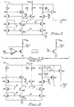
- Such "quasi-devices” often are used in source-follower configurations as shown in Fig. 1A hereof.
- Output stages comprised of quasi-devices have low output impedance, as do source followers, and have the further advantage of larger output voltage swings than source followers.
- Patent 4,480,230 (Brehmer et al.), additional circuitry is added to a class AB output stage to sense when large quiescent currents are flowing in the output MOSFETs to provide feedback which is used to attenuate the quiescent (no-load) current in the output MOSFETs.
- Patent 5,162,752 (Khorramabadi) discloses use of class B output MOSFETs and class AB output MOSFETs connected in parallel and driven from separate error amplifiers.
- both the Brehmer et al. and Khorramabadi circuits are complex, and neither solves the problem of substantial variation in the amount of quiescent current that flows through the output MOSFETs as a function of typical variations in temperature, power supply voltage, and integrated circuit process parameters.
- the portion 2 of the illustrated bias circuit that includes resistor R1 and MOSFETs M1-M6 constitutes a prior art bias circuit which operates so as to keep MOSFET M1 at the edge of strong inversion, i.e., just at the edge of being turned “on". That bias circuit 2 is commonly used to provide bias voltage on conductors 12 and 13 to drive current mirror output transistors such as M9 and M10 in Fig. 1. Such current mirror output transistors function as a constant current source for a differential amplifier stage 3.
- CMOS output stage which can be used to provide large output voltage swings into low impedance loads and steady DC bias current in the output transistors of such output stage over typical variations in power supply voltage, CMOS processing parameters, and chip temperature.
- the invention provides a CMOS output circuit including a bias circuit (2), the bias circuit including a first resistor (R1) coupled between a first supply voltage conductor (V DD ) and a first conductor (10), a first first-conductivity-type MOSFET (M1) having a source coupled to the first supply voltage conductor (V DD ), a gate coupled to the first conductor (10), and a drain coupled to a second conductor (11), a second first-conductivity-type MOSFET (M2) having a source coupled to the first conductor (10), a gate coupled to the second conductor (11), and a drain coupled to a drain and gate of a first second-conductivity-type current mirror control MOSFET (M3) having a source coupled to a second supply voltage conductor (8), and a first second-conductivity-type current mirror output MOSFET (M5) having a gate coupled to the gate of the first second-conductivity-type current mirror
- the pull-up MOSFETs become pull-down MOSFETs, and the two types of CMOS output circuits can be interconnected to provide a high frequency CMOS push-pull output circuit having very stable quiescent bias current.
- low-impedance CMOS output pull-up circuit 1 includes the above mentioned bias circuit 2 and differential amplifier error circuit 3, and also a P-channel MOSFET M11 which functions as a low-impedance output pull-up transistor.
- Bias circuit 2 includes resistor R1, which may have a resistance of 6 kilohms, connected between V DD and conductor 10.
- Conductor 10 is connected to the gate of P-channel MOSFET M1, the source of which is connected to V DD and the drain of which is connected to conductor 11.
- the channel width and length of MOSFET M1 can be 600 microns and 0.8 microns, respectively.
- Conductor 10 is connected to the source of P-channel MOSFET M2, which has its gate connected to conductor 11 and its drain connected to conductor 12.
- the channel width and length of MOSFET M2 can be 100 microns and 0.6 microns, respectively.
- Conductor 12 is connected to the gate and drain of N-channel MOSFET M3 and to the gate of N-channel MOSFET M5, which has its drain connected to conductor 11.
- the source of MOSFET M3 is connected to conductor 13.
- the gate and drain of N-channel MOSFET M4 are connected to conductor 13 and the source of MOSFET M4 is connected to the ground conductor 8 which may be the most negative supply voltage.
- the source of N-channel MOSFET M6 is connected to ground, and its drain is connected to the source of MOSFET M5.
- the channel width and channel length of each of MOSFETs M3-6 may be 25 microns and 0.6 microns, respectively.
- Error amplifier 3 includes N-channel current source MOSFET M10 having its source connected to ground, its gate connected to conductor 13, and its drain connected to the source of a second N-channel current source M9.
- MOSFET M4 is a current mirror control transistor
- MOSFETs M6 and M10 are current mirror output transistors.
- MOSFET M9 has its gate connected to conductor 12 and its drain connected to the sources of N-channel input MOSFETs M7 and M8.
- MOSFET M10 has its gate connected to conductor 13, its drain connected to the source of MOSFET M9, and its source connected to ground.
- the channel width of MOSFETs M9 and M10 are scaled up by a factor of k from the channel width of MOSFETs M3 and M4, and for a value of k equal to 4, the channel width of MOSFETs M9 and M10 may be 100 microns (the channel length thereof being 0.6 microns, the same as for MOSFETs M3 and M4).
- the gates of input MOSFETs M7 and M8 are connected to conductors 4 and 5, respectively.
- the channel width and length of input MOSFETs 7 and 8 may be 200 microns and 0.6 microns, respectively.
- V IN + and V IN - are applied to input conductors 4 and 5, respectively.
- a load resistor R2 which may have a resistance 2 ⁇ R1/k is connected between V DD and the drain of input MOSFET M7. (Preferably, the resistance of load resistors R2 and R3 is reduced by at least the current scale factor k to increase the bandwidth of pull-up circuit 1.)
- Load resistor R3, which may have the same resistance as load resistor R2, is connected between V DD and conductor 6.
- Conductor 6 is connected to the drain of input MOSFET M8 and to the gate of P-channel output MOSFET M11, which has its source connected to V DD and its drain connected to output conductor 7.
- the current in a first leg including resistor R1 and MOSFETs M2, M3, and M4 is approximately equal to the P-channel threshold voltage V TP of MOSFET M1 divided by the resistance R1 of resistor R1.
- the current flowing through a second leg including MOSFETs M1, M5, and M6 is identical to that in the first leg because the current through current mirror output transistor M6 is the same as the current through current mirror control transistor M4.
- the value of R1 is selected so that MOSFET M1 is biased just at the onset of strong inversion, i.e., so it is just beginning to conduct a significant amount of current.
- output MOSFET M11 can be designed to have a large channel-width-to-channel-length ratio (much larger than that of MOSFET M1) and therefore provide a low output impedance without fear of excessively high quiescent bias currents for worst case values of V DD , MOSFET threshold voltages, and other CMOS process parameters.
- the pull-up output circuit 1 of Fig. 1 would have its output conductor 7 connected to a load circuit (not shown) and also to a pull-down output circuit that is identical to pull-up driver circuit 1 except that the circuit structure is "inverted" between ground and V DD in the sense that the various P-channel MOSFETS are replaced with corresponding N-channel MOSFETs, and the N-channel MOSFETs are replaced with corresponding P-channel MOSFETs.
- MOSFET M1 be physically located as close as possible to output MOSFET M11, preferably with both MOSFETs M1 and M11 located relative to each other on a common thermal centroid, to ensure that the temperature of bias MOSFET M1 accurately tracks the temperature of pull-up MOSFET M11 during operation.
- biasing of pull-up MOSFET M11 is dependent upon the input offset voltage of error amplifier 3. That input offset voltage is dependent upon the matching between input MOSFETs M7 and M8, especially the threshold voltages thereof, and also on the degree of matching between load resistors R2 and R3. If the polarity of such input offset voltage is such that it increases the current through input MOSFET M8, then the quiescent bias current through pull-up MOSFET M11 also will increase, and the increase may be dramatic (e.g., by a factor as of much as 10), if the designed value of quiescent current lies on a steep part of the I DRAIN verses V GS characteristic of MOSFET 11.
- resistor R5 is connected between conductors 6 and 15.
- Pull-up MOSFET M11' of Fig. 2 replaces MOSFET M11 of Fig. 1 (and is connected exactly the same as MOSFET 11).
- an additional P-channel pull-up MOSFET M12 has its source electrode connected to V DD , its drain electrode connected to conductor 7, and its gate connected to conductor 15.
- the output pull-up MOSFET 11 of Fig. 1 is "split" into the two parallel connected P-channel MOSFET pull-ups M11' and M12.
- the channel-length-to-channel-width ratio of pull-up MOSFET M12 is much larger (e.g., ten times larger) than that of pull-up MOSFET M11'.
- the resistance of resistor R5 typically is much smaller than the resistance of resistor R4.
- the resistance of R5 can be 2 ⁇ c ⁇ R1/k
- the resistance of resistor R4 can be 2(1-c)R1/k, c being a scale factor which determines the relationship between resistors R4 and R5 and is chosen so that pull-up transistor M12 is never turned on too strongly under quiescent (i.e., no-load) conditions over a reasonable range of error amplifier input offset voltages.
- c can have a value of 0.05. Even though pull-up MOSFET M11' may be turned on too strongly as a result of error amplifier offset voltage, its size is greatly reduced compared to that of MOSFET M11 of Fig. 1. The configuration of Fig. 2 prevents the sum of the quiescent bias currents in both MOSFETs M11' and M12 from being too great.
- Fig. 2 overcomes the problem of heavy dependency of the quiescent current through the output pull-up MOSFETs on the input offset voltage of the error amplifier 3, the amount of available "gate drive" to produce the gate-to-source voltage of the pull-up MOSFETs M11' and M12 is determined by the portions of the bias current from MOSFETs M9 and M10 flowing through each of pull-up resistors R4 and R5. For the above indicated values of R2, R4 and R5 in Fig.
- the output stage 1B of Fig. 3 provides a solution to this problem by unbalancing the currents through MOSFETS M7 and M8 so that only one fourth of the current supplied by MOSFET M10 flows through MOSFET M8 and the rest flows through MOSFET M7.
- the output pull-up circuit 1B is identical to circuit 1A of Fig. 2 except the relationship between the resistance of the error amplifier resistor load circuits R2 and R4+R5 is modified and the relative geometries of input MOSFETS M7 and M8 also are similarly modified. Specifically, load resistors R4 (having resistance 2(1-c)R1/k) and R5 (having resistance 2cR1/k) of Fig. 2 are replaced by load resistors R6 (having resistance 2(1-c)R1/(k(1-e)) and R7 (having resistance 2cR1/(k(1-e)) in Fig. 3, respectively, where e is a scale factor which may have a value of 0.5.
- Load resistor R2 (having resistance 2R1/k) of Fig. 2 is replaced by load resistor R2' (having resistance 2R1/(k(1+e)) in Fig. 3.
- Input MOSFETs M7 and M8, (both having a channel width WD) are replaced by N-channel input MOSFETs M13 (with a channel width of (1+e)WD)) and M14 (with a channel width of (1-e)WD), respectively, where WD is the width of MOSFETs M7 and M8 in Fig. 2.
- the two branches of differential error amplifier 3 in Fig. 3 are unbalanced according to the scale factor e so that under quiescent conditions (i.e., V IN + is equal to V IN - ) significantly more current flows through input MOSFET M13 than through input MOSFET M14.
- the unbalance is achieved by multiplying the width of MOSFET M7 of Fig. 2 by the factor 1+e to obtain the channel width of MOSFET M13, dividing the resistance of resistor R2 of Fig. 2 by the factor 1+e to obtain the resistance of resistor R2' in Fig. 3, multiplying the width of MOSFET M8 in Fig. 2 by the factor 1-e to obtain the channel width of MOSFET M14 of Fig.
- the increased available maximum gate drive voltage on conductors 6 and 15 allows use of significantly smaller transistors for pull-up MOSFETS M11' and M12. This reduces the gate capacitances of pull-up MOSFETs M11' and M12, reducing the associated RC time constants and increasing the circuit bandwidth while providing the desired low impedance and low maximum total quiescent bias current of both pull-up transistors M11' and M12 under worst case temperature variations (-40°C to +125°C) and CMOS process paramater variations.
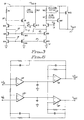
- Fig. 4 shows a connection of output driver circuit 1B of Fig. 3 and a second "complementary" output driver circuit 1B' in which the V DD and ground connectors and the channel types of all MOSFETs of output driver circuit 1B have been reversed to provide a pull-down output stage circuit, whereby a push-pull output stage is provided.
- the widths of such "reversed" N-channel MOSFETs which have substituted for P-channel MOSFETs and vice versa to obtain the complementary output driver circuit 1B' should, of course, be adjusted to account for the different conductivities of N-channel and P-channel MOSFEtS. Additional MOSFETs, resistors and PNP transistors have been added as shown in blocks 20 and 20' to ensure start-up of the bias circuits 2 and 2'.
- the circuit 1B of Fig. 4 can be used with a high gain differential preamplifier 21 to provide the buffer amplifier shown in Fig. 5.
- Two output drivers 1B and 1B' as shown in Fig. 4 can be combined with two preamplifiers 21 and 21' to provide a differential buffer circuit shown in Fig. 6.
- the circuit shown in Fig. 6 has been tested.
- the present invention solves the shortcomings of the closest prior art by controlling the quiescent current through the output pull-up and pull-down transistors by means of components which already are part of the signal path, rather than by adding additional bias sensing control circuitry, and by establishing the quiescent bias current in response to a reference device the performance of which tracks closely with the temperature and CMOS processing parameters of the output MOSFETs through which the load currents flow. Low crossover distortion and good linearity of V OUT are achieved because of the essentially constant quiescent bias current is the output MOSFETs.
Landscapes
- Engineering & Computer Science (AREA)
- Power Engineering (AREA)
- Amplifiers (AREA)
- Manipulation Of Pulses (AREA)
Claims (5)
- Eine CMOS-Ausgangsschaltung mit einer Vorspannungsschaltung (2), wobei die Vorspannungsschaltung einen ersten Widerstand (R1) enthält, der zwischen einen ersten Versorgungsspannungsleiter (VDD) und einen ersten Leiter (10) gekoppelt ist, einen ersten MOSFET (M1) eines ersten Leitfähigkeitstyps mit einer mit dem ersten Versorgungsspannungsleiter (VDD) gekoppelten Source, einem mit dem ersten Leiter (10) gekoppelten Gate und einem mit einem zweiten Leiter (11) gekoppelten Drain, einen zweiten MOSFET (M2) eines ersten Leitfähigkeitstyps mit einer mit dem ersten Leiter (10) gekoppelten Source, einem mit dem zweiten Leiter (11) gekoppelten Gate und einem mit einem Drain und einem Gate eines ersten Stromspiegelsteuerungs-MOSFET (M3) eines zweiten Leitfähigkeitstyps, der eine Source aufweist, die mit einem zweiten Versorgungsspannungsleiter (8) gekoppelt ist, und einen ersten Stromspiegel-Ausgabe-MOSFET (M5) eines zweiten Leitfähigkeitstyps, der ein Gate aufweist, das mit dem Gate des ersten Stromspiegelsteuerungs-MOSFET (M3) eines zweiten Leitfähigkeitstyps gekoppelt ist, eine Source, die mit dem zweiten Versorgungsspannungsleiter (8) gekoppelt ist, und einen mit dem zweiten Leiter (11) gekoppelten Drain, gekennzeichnet durch:wobei eine Spannung, die durch den Fehlerverstärker auf dem Gate des zweiten Ausgabe-MOSFET (M12) eines ersten Leitfähigkeitstyps erzeugt wird, einen stabilen Ruhevorspannungsstrom im zweiten Ausgabe-MOSFET (M12) eines ersten Leitfähigkeitstyps erzeugt, der ein vorbestimmtes Vielfaches eines Vorspannungsstroms ist, der durch den ersten MOSFET (M1) eines ersten Leitfähigkeitstyps fließt, um zu veranlassen, dass der zweite Ausgabe-MOSFET (M12) eines ersten Leitfähigkeitstyps an der Grenze seines Zustands einer starken Inversion ähnlich dem ersten MOSFET (M1) des ersten Leitfähigkeitstyps vorgespannt wird.(a) einen Fehlerverstärker (3) miti. einem ersten (M7) und zweiten (M8) Eingabe-MOSFET eines zweiten Leitfähigkeitstyps, wobei ein Gate des ersten Eingabe-MOSFET (M7) eines zweiten Leitfähigkeitstyps mit einem ersten Eingangsanschluss (4) gekoppelt ist und ein Gate des zweiten Eingabe-MOSFET (M8) eines zweiten Leitfähigkeitstyps mit einem zweiten Eingangsanschluss (5) gekoppelt ist,ii. einem zweiten Stromspiegel-Ausgangstransistor (M9) eines zweiten Leitfähigkeitstyps mit einem Gate, das mit dem Gate des ersten Stromspiegelsteuerungs-MOSFET (M3) eines zweiten Leitfähigkeitstyps gekoppelt ist, einer Source, die mit dem zweiten Versorgungsspannungsleiter (8) gekoppelt ist, und einem Drain, der mit Sources des ersten (M7) und zweiten (M8) Eingabe-MOSFET eines zweiten Leitfähigkeitstyps gekoppelt ist, undiii. einer ersten ohmschen Last (R2), die zwischen den ersten Versorgungsspannungsleiter (VDD) und einen Drain des ersten Eingabe-MOSFET (M7) eines zweiten Leitfähigkeitstyps gekoppelt ist,iv. einer zweiten ohmschen Last (R5), die zwischen einen Drain des zweiten Eingabe-MOSFET (M8) eines zweiten Leitfähigkeitstyps und einen dritten Leiter (15) gekoppelt ist,v, einer dritten ohmschen Last (R4), die zwischen den dritten Leiter (15) und den ersten Versorgungsspannungsleiter (VDD) gekoppelt ist;(b) einen ersten Ausgabe-MOSFET (M11') eines ersten Leitfähigkeitstyps mit einem Gate, das mit dem Drain des zweiten Eingabe-MOSFET (M8) eines zweiten Leitfähigkeitstyps gekoppelt ist, einer Source, die mit dem ersten Versorgungsspannungsleiter (VDD) gekoppelt ist, und einem mit einem Ausgangsanschluss (7) gekoppelten Drain;(c) einen zweiten Ausgabe-MOSFET (M12) eines ersten Leitfähigkeitstyps mit einer Source, die mit dem ersten Versorgungsspannungsleiter (VDD) gekoppelt ist, einem Gate, das mit dem dritten Leiter (15) gekoppelt ist, und einem mit dem Ausgangsleiter (7) gekoppelten Drain,
- CMOS-Ausgangsschaltung nach Anspruch 1, worin der erste Leitfähigkeitstyp ein P-Typ ist und der zweite Leitfähigkeitstyp ein N-Typ ist und der Ausgabe-MOSFET ein Pull-Up-MOSFET ist.
- CMOS-Ausgangsschaltung nach Anspruch 1, worin der erste Leitfähigkeitstyp ein N-Typ ist, der zweite Leitfähigkeitstyp ein P-Typ ist und der Ausgabe-MOSFET ein Pull-Down-MOSFET ist.
- CMOS-Ausgangsschaltung nach einem der Ansprüche-1 bis 3, worin das Verhältnis von Kanalbreite zu Kanallänge des ersten Ausgabe-MOSFET (M11') eines ersten Leitfähigkeitstyps im wesentlichen geringer als das Verhältnis von Kanalbreite zur Kanallänge des zweiten Ausgabe-MOSFET (M12) eines ersten Leitfähigkeitstyps ist, um zu verhindern, dass ein Ruhevorspannungsstrom im ersten Ausgabe-MOSFET (M11') eines ersten Leitfähigkeitstyps im Falle einer großen Eingangs-Offsetspannung im Fehlerverstärker (3) übermäßig groß wird.
- CMOS-Ausgangsschaltung nach Anspruch 4, worin die erste ohmsche Last (R2) einen Widerstandswert hat, der dem Widerstandswert des ersten Widerstands proportional ist, geteilt durch einen ersten Skalenfaktor k, die zweite ohmsche Last (R5) einen Widerstandswert hat, der einem zweiten Skalenfaktor c multipliziert mit dem Widerstandswert des ersten Widerstands geteilt durch den ersten Skalenfaktor k proportional ist, und die dritte ohmsche Last (R4) einen Widerstandswert hat, der dem Widerstandswert des ersten Widerstands multipliziert mit (1-c)/k proportional ist, um den zweiten Ausgabe-MOSFET eines ersten Leitfähigkeitstyps an der Grenze seines Zustands einer starken Inversion ähnlich dem ersten MOSFET eines ersten Leitfähigkeitstyps vorzuspannen.
Applications Claiming Priority (3)
| Application Number | Priority Date | Filing Date | Title |
|---|---|---|---|
| US743006 | 1991-08-09 | ||
| US08/743,006 US5856749A (en) | 1996-11-01 | 1996-11-01 | Stable output bias current circuitry and method for low-impedance CMOS output stage |
| PCT/US1997/016444 WO1998020610A1 (en) | 1996-11-01 | 1997-09-15 | Low-impedance cmos output stage and method |
Publications (3)
| Publication Number | Publication Date |
|---|---|
| EP0935849A1 EP0935849A1 (de) | 1999-08-18 |
| EP0935849A4 EP0935849A4 (de) | 2002-04-17 |
| EP0935849B1 true EP0935849B1 (de) | 2004-09-15 |
Family
ID=24987146
Family Applications (1)
| Application Number | Title | Priority Date | Filing Date |
|---|---|---|---|
| EP97944313A Expired - Lifetime EP0935849B1 (de) | 1996-11-01 | 1997-09-15 | Leistungsendstufenschaltung mit niedriger impedanz sowie verfahren |
Country Status (7)
| Country | Link |
|---|---|
| US (2) | US5856749A (de) |
| EP (1) | EP0935849B1 (de) |
| JP (1) | JP3251019B2 (de) |
| DE (1) | DE69730724T2 (de) |
| IL (1) | IL129520A0 (de) |
| TW (1) | TW359893B (de) |
| WO (1) | WO1998020610A1 (de) |
Families Citing this family (33)
| Publication number | Priority date | Publication date | Assignee | Title |
|---|---|---|---|---|
| JP3304539B2 (ja) * | 1993-08-31 | 2002-07-22 | 富士通株式会社 | 基準電圧発生回路 |
| US5856749A (en) * | 1996-11-01 | 1999-01-05 | Burr-Brown Corporation | Stable output bias current circuitry and method for low-impedance CMOS output stage |
| IT1291676B1 (it) * | 1997-04-28 | 1999-01-19 | Sgs Thomson Microelectronics | Stadio di uscita a cmos esente da fenomeni di deriva |
| US6102962A (en) * | 1997-09-05 | 2000-08-15 | Lsi Logic Corporation | Method for estimating quiescent current in integrated circuits |
| US6986788B2 (en) * | 1998-01-30 | 2006-01-17 | Synthes (U.S.A.) | Intervertebral allograft spacer |
| US6037807A (en) * | 1998-05-18 | 2000-03-14 | Integrated Device Technology, Inc. | Synchronous sense amplifier with temperature and voltage compensated translator |
| JP3476363B2 (ja) * | 1998-06-05 | 2003-12-10 | 日本電気株式会社 | バンドギャップ型基準電圧発生回路 |
| US6525598B1 (en) | 1999-01-29 | 2003-02-25 | Cirrus Logic, Incorporated | Bias start up circuit and method |
| US6465999B2 (en) | 2000-02-11 | 2002-10-15 | Advanced Analogic Technologies, Inc. | Current-limited switch with fast transient response |
| US6166530A (en) * | 2000-02-11 | 2000-12-26 | Advanced Analogic Technologies, Inc. | Current-Limited switch with fast transient response |
| US6448821B1 (en) * | 2000-02-25 | 2002-09-10 | National Semiconductor Corporation | Comparator circuit for comparing differential input signal with reference signal and method |
| US6369652B1 (en) * | 2000-05-15 | 2002-04-09 | Rambus Inc. | Differential amplifiers with current and resistance compensation elements for balanced output |
| US6605993B2 (en) * | 2000-05-16 | 2003-08-12 | Fujitsu Limited | Operational amplifier circuit |
| DE60034131T2 (de) | 2000-12-04 | 2008-01-24 | Infineon Technologies Ag | Treiber für einen externen Feldeffekttransistor mit hoher Genauigkeit und Gate-Spannungsschutz |
| FR2825806B1 (fr) * | 2001-06-08 | 2003-09-12 | St Microelectronics Sa | Circuit de polarisation a point de fonctionnement stable en tension et en temperature |
| US7012465B2 (en) * | 2001-08-07 | 2006-03-14 | Qualcomm Incorporated | Low-voltage class-AB output stage amplifier |
| US6590453B2 (en) * | 2001-09-21 | 2003-07-08 | Silicon Storage Technology, Inc. | Folded cascode high voltage operational amplifier with class AB source follower output stage |
| JP4009214B2 (ja) * | 2003-03-14 | 2007-11-14 | 松下電器産業株式会社 | 電流駆動装置 |
| US7057444B2 (en) * | 2003-09-22 | 2006-06-06 | Standard Microsystems Corporation | Amplifier with accurate built-in threshold |
| US7321516B2 (en) * | 2004-02-19 | 2008-01-22 | Stmicroelectronics, S.R.L. | Biasing structure for accessing semiconductor memory cell storage elements |
| US7109697B1 (en) * | 2005-06-29 | 2006-09-19 | Texas Instruments Incorporated | Temperature-independent amplifier offset trim circuit |
| US7345465B2 (en) * | 2006-06-12 | 2008-03-18 | Intersil Americas Inc. | Two pin-based sensing of remote DC supply voltage differential using precision operational amplifier and diffused resistors |
| US8391812B2 (en) * | 2009-08-27 | 2013-03-05 | Sige Semiconductor, Inc. | Method and system for amplifier control |
| US20120319241A1 (en) * | 2011-06-17 | 2012-12-20 | Analog Devices, Inc. | Offset reducing resistor circuit |
| US20130064027A1 (en) * | 2011-09-14 | 2013-03-14 | Meng-Yi Wu | Memory and Method of Adjusting Operating Voltage thereof |
| US8742800B1 (en) * | 2012-09-27 | 2014-06-03 | Maxim Integrated Products, Inc. | Integrated circuit with precision current source |
| US9148140B1 (en) | 2012-09-27 | 2015-09-29 | Maxim Integrated Systems, Inc. | Integrated circuit with precision current source |
| US9088252B2 (en) | 2013-03-05 | 2015-07-21 | Richwave Technology Corp. | Fixed voltage generating circuit |
| US20140253087A1 (en) * | 2013-03-05 | 2014-09-11 | Richwave Technology Corp. | Fixed voltage generating circuit |
| GB2512916A (en) * | 2013-04-11 | 2014-10-15 | Nujira Ltd | Output stage for class AB amplifier |
| US10186942B2 (en) * | 2015-01-14 | 2019-01-22 | Dialog Semiconductor (Uk) Limited | Methods and apparatus for discharging a node of an electrical circuit |
| CN105116954B (zh) * | 2015-09-07 | 2017-09-01 | 卓捷创芯科技(深圳)有限公司 | 一种宽输入电压范围和高精度输出的自偏置带隙基准电路 |
| CN120222801B (zh) * | 2025-02-12 | 2026-01-27 | 广州润芯信息技术有限公司 | 一种输出限幅装置 |
Family Cites Families (28)
| Publication number | Priority date | Publication date | Assignee | Title |
|---|---|---|---|---|
| US4284957A (en) * | 1979-09-28 | 1981-08-18 | American Microsystems, Inc. | CMOS Operational amplifier with reduced power dissipation |
| US4335355A (en) * | 1979-09-28 | 1982-06-15 | American Microsystems, Inc. | CMOS Operational amplifier with reduced power dissipation |
| US4383223A (en) * | 1980-04-10 | 1983-05-10 | Motorola, Inc. | CMOS Operational amplifier employing push-pull output stage |
| US4333058A (en) * | 1980-04-28 | 1982-06-01 | Rca Corporation | Operational amplifier employing complementary field-effect transistors |
| US4484148A (en) * | 1982-09-13 | 1984-11-20 | National Semiconductor Corporation | Current source frequency compensation for a CMOS amplifier |
| US4480230A (en) * | 1983-07-05 | 1984-10-30 | National Semiconductor Corporation | Large swing CMOS power amplifier |
| JP2525346B2 (ja) * | 1983-10-27 | 1996-08-21 | 富士通株式会社 | 定電流源回路を有する差動増幅回路 |
| SU1246339A1 (ru) * | 1984-12-17 | 1986-07-23 | Предприятие П/Я А-3390 | Дифференциальный усилитель |
| JPS61148906A (ja) * | 1984-12-24 | 1986-07-07 | Hitachi Ltd | Mos増幅出力回路 |
| JPS61156910A (ja) * | 1984-12-28 | 1986-07-16 | Fujitsu Ltd | 差動増幅回路 |
| US4656436A (en) * | 1985-12-31 | 1987-04-07 | At&T Bell Laboratories | CMOS transconductance circuit with triode mode input |
| JP2594585B2 (ja) * | 1987-11-25 | 1997-03-26 | 富士通株式会社 | 演算増幅回路 |
| US4897612A (en) * | 1988-05-09 | 1990-01-30 | National Semiconductor Corporation | Operational transconductance amplifier with improved current source capability |
| JPH0682997B2 (ja) * | 1988-06-28 | 1994-10-19 | 日本電気株式会社 | Mos差動増幅回路 |
| JPH0834391B2 (ja) * | 1989-08-01 | 1996-03-29 | 日本電気株式会社 | 演算増幅回路 |
| US5162753A (en) * | 1991-11-27 | 1992-11-10 | At&T Bell Laboratories | Amplifier arrangement for use as a line driver |
| JP3320434B2 (ja) * | 1991-11-28 | 2002-09-03 | 沖電気工業株式会社 | 演算増幅回路 |
| JPH05289760A (ja) * | 1992-04-06 | 1993-11-05 | Mitsubishi Electric Corp | 基準電圧発生回路 |
| US5220288A (en) * | 1992-06-01 | 1993-06-15 | Motorola, Inc. | Continuous-time differential amplifier with low offset voltage |
| US5287070A (en) * | 1992-09-02 | 1994-02-15 | Ncr Corporation | Balanced voltage comparator |
| JPH06104672A (ja) * | 1992-09-22 | 1994-04-15 | Mitsubishi Electric Corp | クランプ回路 |
| US5363059A (en) * | 1993-06-17 | 1994-11-08 | Texas Instruments Incorporated | Transconductance amplifier |
| US5446412A (en) * | 1994-05-19 | 1995-08-29 | Exar Corporation | Continuously linear pulse amplifier/line driver with large output swing |
| US5491448A (en) * | 1994-07-29 | 1996-02-13 | National Semiconductor Corporation | Class AB output stage with improved frequency stability |
| US5500624A (en) * | 1994-11-02 | 1996-03-19 | Motorola, Inc. | Input stage for CMOS operational amplifier and method thereof |
| US5515006A (en) * | 1995-03-07 | 1996-05-07 | Linfinity Microelectronics, Inc. | Low distortion efficient large swing CMOS amplifier output |
| US5596289A (en) * | 1995-05-15 | 1997-01-21 | National Science Council | Differential-difference current conveyor and applications therefor |
| US5856749A (en) * | 1996-11-01 | 1999-01-05 | Burr-Brown Corporation | Stable output bias current circuitry and method for low-impedance CMOS output stage |
-
1996
- 1996-11-01 US US08/743,006 patent/US5856749A/en not_active Expired - Lifetime
-
1997
- 1997-09-15 WO PCT/US1997/016444 patent/WO1998020610A1/en not_active Ceased
- 1997-09-15 DE DE69730724T patent/DE69730724T2/de not_active Expired - Lifetime
- 1997-09-15 IL IL12952097A patent/IL129520A0/xx unknown
- 1997-09-15 JP JP52137498A patent/JP3251019B2/ja not_active Expired - Fee Related
- 1997-09-15 EP EP97944313A patent/EP0935849B1/de not_active Expired - Lifetime
- 1997-10-29 TW TW086116085A patent/TW359893B/zh not_active IP Right Cessation
-
1998
- 1998-12-16 US US09/213,333 patent/US6002276A/en not_active Expired - Lifetime
Also Published As
| Publication number | Publication date |
|---|---|
| DE69730724D1 (de) | 2004-10-21 |
| WO1998020610A1 (en) | 1998-05-14 |
| DE69730724T2 (de) | 2006-02-16 |
| EP0935849A4 (de) | 2002-04-17 |
| US6002276A (en) | 1999-12-14 |
| EP0935849A1 (de) | 1999-08-18 |
| US5856749A (en) | 1999-01-05 |
| IL129520A0 (en) | 2000-02-29 |
| TW359893B (en) | 1999-06-01 |
| JP2000507787A (ja) | 2000-06-20 |
| JP3251019B2 (ja) | 2002-01-28 |
Similar Documents
| Publication | Publication Date | Title |
|---|---|---|
| US6002276A (en) | Stable output bias current circuitry and method for low-impedance CMOS output stage | |
| US4857863A (en) | Low power output driver circuit with slew rate limiting | |
| US5220207A (en) | Load current monitor for MOS driver | |
| US5804994A (en) | Comparator circuit with hysteresis | |
| KR0131334B1 (ko) | 증폭기 회로 | |
| JPS63107210A (ja) | 差電圧−電流変換器 | |
| EP1908168B1 (de) | Temperaturunabhängige verstärker-offsettrimmschaltung | |
| US7196581B2 (en) | Amplifier switching control circuit and method for current shunt instrumentation amplifier having extended position and negative input common mode range | |
| EP0240114B1 (de) | Komparator zum Vergleich zweier Eingangssignale und Verfahren dazu | |
| US4596958A (en) | Differential common base amplifier with feed forward circuit | |
| US6717451B1 (en) | Precision analog level shifter with programmable options | |
| US4371844A (en) | Differential load circuit equipped with field-effect transistors | |
| KR20020056830A (ko) | 증폭기 | |
| US5442319A (en) | Active biasing control for class-AB CMOS operational amplifiers | |
| US5994926A (en) | Circuit and method for programmably changing the transconductance of a transconductor circuit | |
| US6940353B2 (en) | High frequency power amplifier | |
| EP0711032A1 (de) | Eingangsstufe für CMOS-Operationsverstärker und Verfahren dazu | |
| US5684432A (en) | Amplifier output stage having enhanced drive capability | |
| EP0426598B1 (de) | Transistorverstärker mit veränderlichen Vorspannungsschaltungen | |
| US5426396A (en) | Differential amplifier multiplexer | |
| US6633441B1 (en) | Method and apparatus for measuring an output signal of a floating transducer | |
| US20060033570A1 (en) | Differential amplifier | |
| US5754079A (en) | Method and apparatus for biasing a differential cascode circuit | |
| JPH09153747A (ja) | 差動増幅器の同相電圧帰還回路 | |
| KR0157954B1 (ko) | 전류구동회로 |
Legal Events
| Date | Code | Title | Description |
|---|---|---|---|
| PUAI | Public reference made under article 153(3) epc to a published international application that has entered the european phase |
Free format text: ORIGINAL CODE: 0009012 |
|
| 17P | Request for examination filed |
Effective date: 19990428 |
|
| AK | Designated contracting states |
Kind code of ref document: A1 Designated state(s): DE FR GB IT NL |
|
| A4 | Supplementary search report drawn up and despatched |
Effective date: 20020307 |
|
| AK | Designated contracting states |
Kind code of ref document: A4 Designated state(s): DE FR GB IT NL |
|
| RIC1 | Information provided on ipc code assigned before grant |
Free format text: 7H 03K 5/22 A, 7H 03F 3/45 B, 7H 03F 3/30 B |
|
| 17Q | First examination report despatched |
Effective date: 20030514 |
|
| GRAP | Despatch of communication of intention to grant a patent |
Free format text: ORIGINAL CODE: EPIDOSNIGR1 |
|
| RAP1 | Party data changed (applicant data changed or rights of an application transferred) |
Owner name: TEXAS INSTRUMENTS TUCSON CORPORATION |
|
| GRAS | Grant fee paid |
Free format text: ORIGINAL CODE: EPIDOSNIGR3 |
|
| GRAA | (expected) grant |
Free format text: ORIGINAL CODE: 0009210 |
|
| AK | Designated contracting states |
Kind code of ref document: B1 Designated state(s): DE FR GB IT NL |
|
| PG25 | Lapsed in a contracting state [announced via postgrant information from national office to epo] |
Ref country code: NL Free format text: LAPSE BECAUSE OF FAILURE TO SUBMIT A TRANSLATION OF THE DESCRIPTION OR TO PAY THE FEE WITHIN THE PRESCRIBED TIME-LIMIT Effective date: 20040915 Ref country code: IT Free format text: LAPSE BECAUSE OF FAILURE TO SUBMIT A TRANSLATION OF THE DESCRIPTION OR TO PAY THE FEE WITHIN THE PRE;WARNING: LAPSES OF ITALIAN PATENTS WITH EFFECTIVE DATE BEFORE 2007 MAY HAVE OCCURRED AT ANY TIME BEFORE 2007. THE CORRECT EFFECTIVE DATE MAY BE DIFFERENT FROM THE ONE RECORDED.SCRIBED TIME-LIMIT Effective date: 20040915 |
|
| REG | Reference to a national code |
Ref country code: GB Ref legal event code: FG4D |
|
| REF | Corresponds to: |
Ref document number: 69730724 Country of ref document: DE Date of ref document: 20041021 Kind code of ref document: P |
|
| NLV1 | Nl: lapsed or annulled due to failure to fulfill the requirements of art. 29p and 29m of the patents act | ||
| ET | Fr: translation filed | ||
| PLBE | No opposition filed within time limit |
Free format text: ORIGINAL CODE: 0009261 |
|
| STAA | Information on the status of an ep patent application or granted ep patent |
Free format text: STATUS: NO OPPOSITION FILED WITHIN TIME LIMIT |
|
| 26N | No opposition filed |
Effective date: 20050616 |
|
| PGFP | Annual fee paid to national office [announced via postgrant information from national office to epo] |
Ref country code: GB Payment date: 20120829 Year of fee payment: 16 |
|
| PGFP | Annual fee paid to national office [announced via postgrant information from national office to epo] |
Ref country code: FR Payment date: 20120910 Year of fee payment: 16 |
|
| PGFP | Annual fee paid to national office [announced via postgrant information from national office to epo] |
Ref country code: DE Payment date: 20120928 Year of fee payment: 16 |
|
| GBPC | Gb: european patent ceased through non-payment of renewal fee |
Effective date: 20130915 |
|
| REG | Reference to a national code |
Ref country code: DE Ref legal event code: R119 Ref document number: 69730724 Country of ref document: DE Effective date: 20140401 |
|
| REG | Reference to a national code |
Ref country code: FR Ref legal event code: ST Effective date: 20140530 |
|
| PG25 | Lapsed in a contracting state [announced via postgrant information from national office to epo] |
Ref country code: GB Free format text: LAPSE BECAUSE OF NON-PAYMENT OF DUE FEES Effective date: 20130915 |
|
| PG25 | Lapsed in a contracting state [announced via postgrant information from national office to epo] |
Ref country code: DE Free format text: LAPSE BECAUSE OF NON-PAYMENT OF DUE FEES Effective date: 20140401 Ref country code: FR Free format text: LAPSE BECAUSE OF NON-PAYMENT OF DUE FEES Effective date: 20130930 |