US6940353B2 - High frequency power amplifier - Google Patents
High frequency power amplifier Download PDFInfo
- Publication number
- US6940353B2 US6940353B2 US10/688,049 US68804903A US6940353B2 US 6940353 B2 US6940353 B2 US 6940353B2 US 68804903 A US68804903 A US 68804903A US 6940353 B2 US6940353 B2 US 6940353B2
- Authority
- US
- United States
- Prior art keywords
- input
- output
- inverter
- coupled
- voltage
- Prior art date
- Legal status (The legal status is an assumption and is not a legal conclusion. Google has not performed a legal analysis and makes no representation as to the accuracy of the status listed.)
- Expired - Lifetime, expires
Links
- 230000003321 amplification Effects 0.000 claims abstract description 7
- 238000003199 nucleic acid amplification method Methods 0.000 claims abstract description 7
- 230000008878 coupling Effects 0.000 claims abstract 5
- 238000010168 coupling process Methods 0.000 claims abstract 5
- 238000005859 coupling reaction Methods 0.000 claims abstract 5
- 230000001105 regulatory effect Effects 0.000 claims abstract 5
- 239000003990 capacitor Substances 0.000 claims description 32
- 239000004065 semiconductor Substances 0.000 claims description 14
- 238000000034 method Methods 0.000 claims description 11
- 230000000295 complement effect Effects 0.000 claims description 8
- 238000001914 filtration Methods 0.000 claims 2
- 238000012544 monitoring process Methods 0.000 claims 2
- 239000013256 coordination polymer Substances 0.000 description 8
- 230000007423 decrease Effects 0.000 description 6
- 230000004044 response Effects 0.000 description 6
- 238000010586 diagram Methods 0.000 description 4
- 229920006395 saturated elastomer Polymers 0.000 description 4
- 230000003247 decreasing effect Effects 0.000 description 3
- 230000001413 cellular effect Effects 0.000 description 2
- 230000000694 effects Effects 0.000 description 1
- 230000010355 oscillation Effects 0.000 description 1
- 230000004043 responsiveness Effects 0.000 description 1
- 238000004513 sizing Methods 0.000 description 1
Images


Classifications
-
- H—ELECTRICITY
- H03—ELECTRONIC CIRCUITRY
- H03F—AMPLIFIERS
- H03F3/00—Amplifiers with only discharge tubes or only semiconductor devices as amplifying elements
- H03F3/30—Single-ended push-pull [SEPP] amplifiers; Phase-splitters therefor
- H03F3/3001—Single-ended push-pull [SEPP] amplifiers; Phase-splitters therefor with field-effect transistors
- H03F3/3022—CMOS common source output SEPP amplifiers
-
- H—ELECTRICITY
- H03—ELECTRONIC CIRCUITRY
- H03F—AMPLIFIERS
- H03F1/00—Details of amplifiers with only discharge tubes, only semiconductor devices or only unspecified devices as amplifying elements
- H03F1/02—Modifications of amplifiers to raise the efficiency, e.g. gliding Class A stages, use of an auxiliary oscillation
- H03F1/0205—Modifications of amplifiers to raise the efficiency, e.g. gliding Class A stages, use of an auxiliary oscillation in transistor amplifiers
- H03F1/0261—Modifications of amplifiers to raise the efficiency, e.g. gliding Class A stages, use of an auxiliary oscillation in transistor amplifiers with control of the polarisation voltage or current, e.g. gliding Class A
-
- H—ELECTRICITY
- H03—ELECTRONIC CIRCUITRY
- H03F—AMPLIFIERS
- H03F1/00—Details of amplifiers with only discharge tubes, only semiconductor devices or only unspecified devices as amplifying elements
- H03F1/34—Negative-feedback-circuit arrangements with or without positive feedback
- H03F1/342—Negative-feedback-circuit arrangements with or without positive feedback in field-effect transistor amplifiers
-
- H—ELECTRICITY
- H03—ELECTRONIC CIRCUITRY
- H03F—AMPLIFIERS
- H03F3/00—Amplifiers with only discharge tubes or only semiconductor devices as amplifying elements
- H03F3/189—High-frequency amplifiers, e.g. radio frequency amplifiers
- H03F3/19—High-frequency amplifiers, e.g. radio frequency amplifiers with semiconductor devices only
-
- H—ELECTRICITY
- H03—ELECTRONIC CIRCUITRY
- H03F—AMPLIFIERS
- H03F2200/00—Indexing scheme relating to amplifiers
- H03F2200/451—Indexing scheme relating to amplifiers the amplifier being a radio frequency amplifier
-
- H—ELECTRICITY
- H03—ELECTRONIC CIRCUITRY
- H03F—AMPLIFIERS
- H03F2200/00—Indexing scheme relating to amplifiers
- H03F2200/555—A voltage generating circuit being realised for biasing different circuit elements
Definitions
- the invention relates to the field of high frequency communications, an in particular to a complementary metal-oxide-semiconductor high frequency amplifier.
- a bipolar transistor In a conventional high-frequency amplifier, a bipolar transistor (or transistors) is used to provide the desired signal gain, while also providing the responsiveness required to maintain signal integrity.
- RF radio-frequency
- One way to reduce costs is to implement the amplifier using a metal-oxide-semiconductor (MOS) or complementary MOS (CMOS) process instead of the more expensive bipolar process.
- MOS metal-oxide-semiconductor
- CMOS complementary MOS
- FIG. 1 shows a conventional MOS RF amplifier 100 .
- MOS amplifier 100 includes an input terminal 101 , an output terminal 102 , capacitors C 1 and C 2 , resistors R_UP, R_DN, and R_SET, and an NMOS transistor 110 .
- Capacitor C 1 is coupled between input terminal 101 and the gate of transistor 110
- capacitor C_OUT is coupled between the drain of transistor 110 and output terminal 102 .
- Resistors R_UP and R_DN are serially coupled between a supply voltage VDD and ground, with the gate of transistor 110 being connected to the junction between the two transistors.
- resistor R_SET and transistor 110 are serially coupled between supply voltage VDD and ground.
- an input RF signal V_IN applied to input terminal 101 is filtered of any DC component by capacitor C 1 and the AC signal is provided to the gate of transistor 110 .
- resistors R_UP and R_DN form a voltage divider that applies a bias voltage to the gate of transistor 110 .
- the bias voltage can be sized such that transistor 110 operates in its linear region in response to the AC signal from capacitor C 1 . Consequently, transistor 110 can apply gain without clipping or otherwise distorting the signal (so long as the input signal is not large enough to force transistor 110 into its saturated region).
- transistor 110 In response to the AC signal at its gate, transistor 110 adjusts the magnitude of the current flow through resistor R_SET, which in turn generates an output signal at the source of transistor 110 . Since the voltage drop across resistor R_SET is equal to the current flow times the resistance of resistor R_SET, the range of the output signal at the source of transistor 110 can be set by selecting an appropriate resistance for resistor R_SET. Increasing or decreasing the resistance of resistor R_SET increases or decreases, respectively, the output range of amplifier 100 .
- the amplified output signal at the source of transistor 110 is then filtered by capacitor C 2 of any DC component that might have been introduced during the amplification process.
- the AC signal is then provided as an output signal V_OUT at output terminal 102 .
- amplifier 100 provides a relatively simple means for RF amplification using a CMOS implementation.
- amplifier 100 can exhibit excessive power consumption. This power inefficiency is generally undesirable, and can be particularly problematic in devices that run off of a self-contained power supply (a battery). For example, using amplifier 100 in a cellular telephone to reduce the overall cost of the phone may result in an unacceptable decrease in talk time for that phone.
- a high-frequency amplifier includes a CMOS inverter and a bias circuit.
- the CMOS inverter applies a gain to an input signal based on the transconductance and output impedance values of the transistors making up the inverter.
- the bias circuit applies linear biasing to the CMOS inverter.
- the bias circuit provides a DC bias voltage to the input of the inverter that forces the output of the inverter to be centered on a desired DC operating voltage.
- the DC bias voltage By selecting the DC bias voltage to be between the upper and lower supply voltages, the inverter can be forced to operate in its linear region.
- An AC (alternating current) signal at the input of the inverter will then be amplified by the inverter without distortion (clipping), so long as the amplitude of the AC signal is not large enough to drive the inverter out of its linear region.
- the bias circuit includes an operational amplifier (op-amp) and a reference voltage source.
- the op-amp is connected in a feedback loop between the output of the inverter and the input of the inverter.
- the reference voltage source provides a reference voltage to the non-inverting input of the op-amp. The op-amp therefore adjusts the input voltage of the inverter in an effort to regulate the output of the inverter to be equal to the reference voltage.
- This DC control provided by the op-amp ensures that the inverter will operate in its linear region as long as the input signal is not large enough to push either of the transistors of the inverter into saturation. Therefore, by setting the reference voltage midway between the upper and lower supply voltages, the output range of the amplifier can be maximized.
- FIG. 1 is a schematic diagram of a conventional CMOS RF amplifier.
- FIG. 2A is a schematic diagram of a CMOS high-frequency amplifier circuit in accordance with an embodiment of the invention.
- FIG. 2B is a sample graph of the response curve of an inverter, depicting the linear and saturated regions of operation of the inverter.
- FIG. 3 is a schematic diagram of the CMOS high-frequency amplifier circuit of FIG. 2A that includes a detail view of a schematic for an operational amplifier in accordance with an embodiment of the invention.
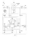
- FIG. 2A shows a high-frequency amplifier circuit 200 in accordance with an embodiment of the invention.
- Amplifier circuit 200 includes an input terminal 201 , an output terminal 202 , a CMOS inverter 210 , a capacitor C_IN, a capacitor C_OUT, and a bias circuit 220 .
- Capacitor C_IN is coupled between input terminal 201 and the input of inverter 210
- capacitor C_OUT is coupled between the output of inverter 210 and output terminal 202 .
- Bias circuit 220 is connected between the output and input of inverter 210 .
- Inverter 210 includes a PMOS transistor M 1 and an NMOS transistor M 2 that are serially coupled between an upper supply voltage VDD and a lower supply voltage VSS (e.g., ground).
- the gate terminals of transistors M 1 and M 2 are connected to form the input of inverter 210
- the drain terminals of transistors M 1 and M 2 are connected to form the output of inverter 210 .
- Amplifier circuit 200 is coupled to receive an input high-frequency signal V_IN at input terminal 201 .
- High-frequency signal V_IN can, for example, comprise an RF signal.
- Capacitor C_IN blocks the DC component of input signal V_IN and passes the AC component to inverter 210 (i.e., capacitor C_IN filters out DC components from input signal V_IN).
- bias circuit 220 provides a feedback loop between the output and input of inverter 210 that applies linear biasing to the input of inverter 210 .
- bias circuit 220 provides a DC bias voltage to the input of inverter 210 that causes inverter 210 to operate in its linear region.
- the DC bias voltage drives a DC operating voltage at the output of inverter 210 to a nominal voltage (a voltage in the absence of an AC signal) between the upper and lower supply voltages of amplifier circuit 200 .
- FIG. 2B shows an exemplary response curve C for inverter 210 .
- Response curve C consists of two main regions—a saturated region that corresponds to all input voltages less than a lower limit voltage V_DN or greater than an upper limit voltage V_UP, and a linear region that corresponds to all input voltages between voltages V_DN and V_UP. Because the normal use of an inverter is to invert a logic LOW or HIGH input signal into a logic HIGH or LOW output signal, respectively, an inverter is generally operated in its saturated region, and will only incidentally pass through its linear region as its output switches between logic LOW (GND) and logic HIGH (VDD).
- bias circuit 220 forces inverter 210 to operate in its linear region, so that inverter 210 can be used to provide signal amplification.
- the DC bias voltage supplied by bias circuit 220 shifts the nominal inverter input voltage (i.e., the voltage at the input of the inverter when no AC signal is present) to a level between lower limit voltage V_DN and upper limit voltage V_UP.
- An AC input signal will therefore swing around this nominal DC input voltage, thereby ensuring that inverter 210 provides an AC output signal that is an amplified value of the AC input signal (so long as the AC input signal amplitude does not exceed lower limit voltage V_DN or upper limit voltage V_UP).
- bias circuit 220 includes resistors R_IN and R_OUT, optional capacitors C 221 and C 222 , a reference voltage source 230 , and an operational amplifier (op-amp) 240 .
- Resistor R_IN is connected between the input of inverter 210 and the output of op-amp 240
- resistor R_OUT is connected between the output of inverter 210 and the non-inverting input of op-amp 240
- Capacitor C 221 is connected between the output of op-amp 240 and lower supply voltage VSS
- capacitor C 222 is connected between the non-inverting input of op-amp 240 and lower supply voltage VSS.
- reference voltage source 230 is connected to the inverting input of op-amp 240 .
- Reference voltage source 230 provides a reference voltage V_MID to the inverting input of op-amp 240 . Meanwhile, the voltage at the output of inverter 210 is provided to the non-inverting input of op-amp 240 (via resistor R_OUT). Therefore, if the voltage at the output of inverter 210 is less than reference voltage V_MID, op-amp 240 decreases its output voltage (and hence the voltage provided at the input of inverter 210 ), thereby raising the output of inverter 210 . Similarly, if the voltage at the output of inverter 210 is greater than reference voltage V_MID, op-amp 240 increases its output voltage to decrease the output of inverter 210 .
- op-amp 240 regulates a DC bias voltage at the input of inverter 210 (via resistor R_IN) to force the output of inverter 210 to swing around a DC operating voltage that is equal to reference voltage V_MID.
- This DC biasing of the input of inverter 210 forces inverter 210 to operate in its linear mode, so that gain can be applied to a signal provided to inverter 210 without distortion (clipping).
- reference voltage V_MID can be set to any value between upper supply voltage VDD and lower supply voltage VSS
- bias circuit 220 includes both resistors R_IN and R_OUT and capacitors C 221 and C 2222 .
- Resistors R_IN and R_OUT effectively isolate op-amp 240 from any AC signals that are provided to or generated by inverter 210 by suppressing the bulk of those signals before they reach op-amp 240 .
- optional capacitors C 221 and C 222 can provide a direct path to lower supply voltage VSS for any AC that does get by resistors R_IN and R_OUT, respectively, or is generated by op-amp 240 .
- bias circuit 220 does not require the resistive divider (voltage divider) of conventional amplifier 100 shown in FIG. 1 , the power consumption of amplifier circuit 200 shown in FIG. 2 can be reduced relative to the power consumption of amplifier 100 .
- inverter 210 can provide a significant amount of gain (while operating in its linear region).
- Ro 2 represents the parallel resistance of Ro 1 and Ro 2 , and resolves to the equation: Ro 1
- Ro 2 ( Ro 1 *Ro 2 )/( Ro 1 +Ro 2 ) (2)
- G ( g m1 +g m2 )/( Y 1 +Y 2 ) (3) where Y 1 is equal to 1/Ro 1 and Y 2 is equal to 1/Ro 2 .
- the transconductance of a transistor represents the relationship between drain current and gate-source voltage in the transistor, and therefore indicates the gain provided by the transistor. The higher the transconductance, the more gain the transistor provides.
- the transconductance is proportional to the aspect ratio (width/length) of the gate. Therefore, by adjusting the gate dimensions of transistors M 1 and M 2 , the gain provided by amplifier circuit 200 can be adjusted.
- upper supply voltage VDD can be 1.8V
- reference voltage V_MID can be set to 0.9V
- lower supply voltage VSS can be ground.
- Transistor M 1 can then have an aspect ratio of 27/0.35
- transistor M 2 can have an aspect ratio of 21.6/0.35
- resistors R_IN and R_OUT can have resistances of 1.5 k ⁇ each
- capacitors C_IN and C_OUT can have capacitances of 150 fF each.
- Amplifier circuit 200 can then provide between 10-15 dB of RF gain.
- amplifier circuit 200 can comprise a stage in a series of cascaded amplifier stages, or a predriver for additional amplifier circuitry, as indicated by optional (dotted line) amplifier stage circuitry 290 .
- FIG. 3 shows another schematic view of high-speed amplifier circuit 200 that depicts a schematic diagram for op-amp 240 , according to an embodiment of the invention.
- Op-amp 240 includes transistors PMOS transistors M 3 and M 5 , NMOS transistors M 4 , M 6 , M 7 , and M 8 , a current source 241 , a capacitor C_CP, and a resistor R_CP.
- Transistors M 3 and M 4 are connected in series between upper supply voltage VDD and transistor M 8 , and transistors M 5 and M 6 are connected in series between upper supply voltage VDD and transistor M 8 .
- Transistor M 8 is coupled between transistor M 4 and lower supply voltage VSS, and current source 241 and transistor M 7 are connected in series between upper supply voltage VDD and lower supply voltage VSS.
- capacitor C_CP and resistor R_CP are connected in series between the gate of transistor M 4 and the drain of transistor M 6 .
- the gate of transistor M 4 forms the non-inverting input of op-amp 240 , and is accordingly coupled to the input of inverter 210 via resistor R_OUT.
- the gate of transistor M 6 forms the inverting input of op-amp 240 , and is therefore coupled to reference voltage circuit 230 .
- the junction between transistors M 5 and M 6 forms the output of op-amp 240 , and is therefore coupled to the input of inverter 210 via resistor R_IN.
- capacitor C_CP and resistor R_CP are coupled between the non-inverting input and the output of op-amp 240 .
- Capacitor C_CP and resistor R_CP form a compensation circuit that improves the stability of op-amp 240 by preventing unwanted oscillations. Note that various other op-amp compensation circuits will be readily apparent.
- transistor M 7 The gate and drain of transistor M 7 are shorted, and the gates of transistors M 7 and M 8 are connected to form a current mirror. Therefore, a current I_BIAS from current source 241 that is sunk by transistor M 7 is also mirrored by transistor M 8 . Therefore, a total current I_BIAS flows through the two branches formed by transistors M 3 and M 4 (first branch) and by transistors M 5 and M 6 (second branch).
- transistor M 3 the gate and drain of transistor M 3 are shorted, and the gates of transistors M 3 and M 5 are connected to form another current mirror that provides a load for the differential pair formed by transistors M 4 and M 6 .
- transistors M 3 and M 5 split the flow of current I_BIAS equally through transistors M 4 and M 6 .
- transistor M 5 adjusts its drain voltage (i.e., the output of op-amp 240 ) in response.
- transistor M 4 For example, if the voltage provided at the gate of transistor M 4 (i.e., the voltage at the output of inverter 210 ) is greater than the voltage provided at the gate of transistor M 6 (i.e., reference voltage V_MID), then transistor M 4 is turned on more strongly than transistor M 6 , and the current flow through transistor M 4 increases. Since the total current flow through transistors M 4 and M 6 is fixed at current I_BIAS by transistor M 8 , this increase in current flow through transistor M 4 means that the current flow through transistor M 6 must decrease.
- the drain voltage of transistor M 6 is increased. This has the effect of reducing the gate-drain voltage of transistor M 6 , which in turn reduces the current flow through transistor M 6 . Meanwhile, this increased drain voltage of transistor M 6 is applied to the input of inverter 210 (via resistor R_IN), thereby driving the voltage at the output of inverter 210 down towards reference voltage V_MID.
- transistor M 4 is turned on less strongly than transistor M 6 , and the current flow through transistor M 4 decreases. Therefore, the current flow through transistor M 6 must increase, and the drain voltage of transistor M 6 is decreased to increase the gate-drain voltage of transistor M 6 .
- This decreased drain voltage of transistor M 6 is applied to the input of inverter 210 , thereby driving the voltage at the output of inverter 210 up towards reference voltage V_MID.
- circuitry shown for op-amp 240 in FIG. 3 is exemplary only. Alternatives may be found in the conventional art.
Landscapes
- Engineering & Computer Science (AREA)
- Power Engineering (AREA)
- Amplifiers (AREA)
Abstract
Description
G=(g m1 +g m2)*(Ro 1 | |Ro 2) (1)
where gm1 and gm2 are the transconductances of transistors M1 and M2, respectively, and Ro1 and Ro2 are the output resistances of transistors M1 and M2, respectively.
Ro 1 | |Ro 2=(Ro 1 *Ro 2)/(Ro 1 +Ro 2) (2)
Substituting equation (2) into equation (1) therefore yields a gain equation of:
G=(g m1 +g m2)/(Y 1 +Y 2) (3)
where Y1 is equal to 1/Ro1 and Y2 is equal to 1/Ro2.
Claims (17)
Priority Applications (1)
| Application Number | Priority Date | Filing Date | Title |
|---|---|---|---|
| US10/688,049 US6940353B2 (en) | 2003-10-16 | 2003-10-16 | High frequency power amplifier |
Applications Claiming Priority (1)
| Application Number | Priority Date | Filing Date | Title |
|---|---|---|---|
| US10/688,049 US6940353B2 (en) | 2003-10-16 | 2003-10-16 | High frequency power amplifier |
Publications (2)
| Publication Number | Publication Date |
|---|---|
| US20050083127A1 US20050083127A1 (en) | 2005-04-21 |
| US6940353B2 true US6940353B2 (en) | 2005-09-06 |
Family
ID=34521092
Family Applications (1)
| Application Number | Title | Priority Date | Filing Date |
|---|---|---|---|
| US10/688,049 Expired - Lifetime US6940353B2 (en) | 2003-10-16 | 2003-10-16 | High frequency power amplifier |
Country Status (1)
| Country | Link |
|---|---|
| US (1) | US6940353B2 (en) |
Cited By (4)
| Publication number | Priority date | Publication date | Assignee | Title |
|---|---|---|---|---|
| US20090021309A1 (en) * | 2004-12-30 | 2009-01-22 | Yuan Jin Zheng | Fully Integrated Ultra Wideband Transmitter Circuits and Systems |
| US7489202B1 (en) | 2007-08-20 | 2009-02-10 | Freescale Semiconductor, Inc. | RF amplifier with stacked transistors, transmitting device, and method therefor |
| US20110089926A1 (en) * | 2009-10-21 | 2011-04-21 | Samsung Electronics Co., Ltd. | Power consumption control method and apparatus for a portable terminal |
| US10587227B2 (en) * | 2015-03-24 | 2020-03-10 | Sony Corporation | Amplifier and electronic circuit |
Families Citing this family (3)
| Publication number | Priority date | Publication date | Assignee | Title |
|---|---|---|---|---|
| US10461738B1 (en) | 2018-05-31 | 2019-10-29 | Qualcomm Incorporated | Comparator architecture and related methods |
| GB202012658D0 (en) * | 2020-08-13 | 2020-09-30 | Nordic Semiconductor Asa | Low noise amplifier |
| US20250385651A1 (en) * | 2024-06-18 | 2025-12-18 | Qualcomm Incorporated | Jammer resilient inductor-less low-noise amplifier for high frequencies |
Citations (6)
| Publication number | Priority date | Publication date | Assignee | Title |
|---|---|---|---|---|
| US4241313A (en) * | 1972-10-27 | 1980-12-23 | Nippon Gakki Seizo Kabushiki Kaisha | Audio power amplifier |
| US4352073A (en) * | 1979-07-13 | 1982-09-28 | Ebauches Electroniques Sa | Complementary MOS field effect transistor amplifier |
| US4943784A (en) * | 1989-03-06 | 1990-07-24 | Motorola, Inc. | Frequency stable digitally controlled driver circuit |
| US5777516A (en) * | 1996-08-13 | 1998-07-07 | Motorola, Inc. | High frequency amplifier in CMOS |
| US6433637B1 (en) * | 2001-03-23 | 2002-08-13 | National Semiconductor Corporation | Single cell rail-to-rail input/output operational amplifier |
| US6836186B2 (en) * | 2002-05-07 | 2004-12-28 | Samsung Electronics Co., Ltd. | AB class amplifier for controlling quiescent current |
-
2003
- 2003-10-16 US US10/688,049 patent/US6940353B2/en not_active Expired - Lifetime
Patent Citations (6)
| Publication number | Priority date | Publication date | Assignee | Title |
|---|---|---|---|---|
| US4241313A (en) * | 1972-10-27 | 1980-12-23 | Nippon Gakki Seizo Kabushiki Kaisha | Audio power amplifier |
| US4352073A (en) * | 1979-07-13 | 1982-09-28 | Ebauches Electroniques Sa | Complementary MOS field effect transistor amplifier |
| US4943784A (en) * | 1989-03-06 | 1990-07-24 | Motorola, Inc. | Frequency stable digitally controlled driver circuit |
| US5777516A (en) * | 1996-08-13 | 1998-07-07 | Motorola, Inc. | High frequency amplifier in CMOS |
| US6433637B1 (en) * | 2001-03-23 | 2002-08-13 | National Semiconductor Corporation | Single cell rail-to-rail input/output operational amplifier |
| US6836186B2 (en) * | 2002-05-07 | 2004-12-28 | Samsung Electronics Co., Ltd. | AB class amplifier for controlling quiescent current |
Cited By (7)
| Publication number | Priority date | Publication date | Assignee | Title |
|---|---|---|---|---|
| US20090021309A1 (en) * | 2004-12-30 | 2009-01-22 | Yuan Jin Zheng | Fully Integrated Ultra Wideband Transmitter Circuits and Systems |
| US7979036B2 (en) * | 2004-12-30 | 2011-07-12 | Agency For Science, Technology And Research | Fully integrated ultra wideband transmitter circuits and systems |
| US7489202B1 (en) | 2007-08-20 | 2009-02-10 | Freescale Semiconductor, Inc. | RF amplifier with stacked transistors, transmitting device, and method therefor |
| US20090051435A1 (en) * | 2007-08-20 | 2009-02-26 | Freescale Semiconductor, Inc. | Rf amplifier with stacked transistors, transmitting device, and method therefor |
| US20110089926A1 (en) * | 2009-10-21 | 2011-04-21 | Samsung Electronics Co., Ltd. | Power consumption control method and apparatus for a portable terminal |
| US8516278B2 (en) * | 2009-10-21 | 2013-08-20 | Samsung Electronics Co., Ltd | Power consumption control method and apparatus for a portable terminal |
| US10587227B2 (en) * | 2015-03-24 | 2020-03-10 | Sony Corporation | Amplifier and electronic circuit |
Also Published As
| Publication number | Publication date |
|---|---|
| US20050083127A1 (en) | 2005-04-21 |
Similar Documents
| Publication | Publication Date | Title |
|---|---|---|
| US7750738B2 (en) | Process, voltage and temperature control for high-speed, low-power fixed and variable gain amplifiers based on MOSFET resistors | |
| US5343164A (en) | Operational amplifier circuit with slew rate enhancement | |
| EP0935849B1 (en) | Low-impedance cmos output stage and method | |
| EP1998438B1 (en) | Differential circuit, amplifier circuit, driver circuit and display device using those circuits | |
| US6288564B1 (en) | Line receiver circuit with line termination impedance | |
| US5381112A (en) | Fully differential line driver circuit having common-mode feedback | |
| US4933644A (en) | Common-mode feedback bias generator for operational amplifiers | |
| US6937071B1 (en) | High frequency differential power amplifier | |
| JPH05251956A (en) | Cascode cmos amplifier with stabilized transient response | |
| US6940353B2 (en) | High frequency power amplifier | |
| US8400214B2 (en) | Class AB output stage | |
| EP1435693A1 (en) | Amplification circuit | |
| WO2004047294A2 (en) | Turn-on bus transmitter with controlled slew rate | |
| KR100468358B1 (en) | Variable Gain Amplifier Having Improved Gain Slope Characteristic | |
| US6977541B2 (en) | Variable time constant circuit and filter circuit using the same | |
| US7391201B2 (en) | Regulated analog switch | |
| US20090027124A1 (en) | Level-Shifting Buffer | |
| KR987001154A (en) | amplifier | |
| US5920217A (en) | 50% Duty cycle signal generator | |
| EP2154783A1 (en) | Amplifying circuit | |
| EP0632582B1 (en) | Operational amplifier and method | |
| US7642867B2 (en) | Simple technique for reduction of gain in a voltage controlled oscillator | |
| US10270392B1 (en) | Low-power differential amplifier with improved unity gain frequency | |
| EP0564225B1 (en) | Voltage generation circuits and methods | |
| US6188284B1 (en) | Distributed gain line driver amplifier including improved linearity |
Legal Events
| Date | Code | Title | Description |
|---|---|---|---|
| AS | Assignment |
Owner name: MICREL, INCORPORATED, CALIFORNIA Free format text: ASSIGNMENT OF ASSIGNORS INTEREST;ASSIGNOR:MORAVEJI, FARHOOD;REEL/FRAME:014618/0421 Effective date: 20031013 |
|
| STCF | Information on status: patent grant |
Free format text: PATENTED CASE |
|
| FPAY | Fee payment |
Year of fee payment: 4 |
|
| FPAY | Fee payment |
Year of fee payment: 8 |
|
| FPAY | Fee payment |
Year of fee payment: 12 |
|
| AS | Assignment |
Owner name: MICROCHIP TECHNOLOGY INCORPORATED, ARIZONA Free format text: INTELLECTUAL PROPERTY BUY-IN AGREEMENT/ASSIGNMENT;ASSIGNOR:MICREL LLC;REEL/FRAME:063241/0771 Effective date: 20151101 |