EP0933950A2 - Farbbildaufnahmegerät - Google Patents
Farbbildaufnahmegerät Download PDFInfo
- Publication number
- EP0933950A2 EP0933950A2 EP99300555A EP99300555A EP0933950A2 EP 0933950 A2 EP0933950 A2 EP 0933950A2 EP 99300555 A EP99300555 A EP 99300555A EP 99300555 A EP99300555 A EP 99300555A EP 0933950 A2 EP0933950 A2 EP 0933950A2
- Authority
- EP
- European Patent Office
- Prior art keywords
- signal
- column
- signals
- row
- image pickup
- Prior art date
- Legal status (The legal status is an assumption and is not a legal conclusion. Google has not performed a legal analysis and makes no representation as to the accuracy of the status listed.)
- Granted
Links
Images


Classifications
-
- H—ELECTRICITY
- H04—ELECTRIC COMMUNICATION TECHNIQUE
- H04N—PICTORIAL COMMUNICATION, e.g. TELEVISION
- H04N25/00—Circuitry of solid-state image sensors [SSIS]; Control thereof
- H04N25/10—Circuitry of solid-state image sensors [SSIS]; Control thereof for transforming different wavelengths into image signals
- H04N25/11—Arrangement of colour filter arrays [CFA]; Filter mosaics
- H04N25/13—Arrangement of colour filter arrays [CFA]; Filter mosaics characterised by the spectral characteristics of the filter elements
- H04N25/135—Arrangement of colour filter arrays [CFA]; Filter mosaics characterised by the spectral characteristics of the filter elements based on four or more different wavelength filter elements
- H04N25/136—Arrangement of colour filter arrays [CFA]; Filter mosaics characterised by the spectral characteristics of the filter elements based on four or more different wavelength filter elements using complementary colours
-
- H—ELECTRICITY
- H04—ELECTRIC COMMUNICATION TECHNIQUE
- H04N—PICTORIAL COMMUNICATION, e.g. TELEVISION
- H04N23/00—Cameras or camera modules comprising electronic image sensors; Control thereof
- H04N23/10—Cameras or camera modules comprising electronic image sensors; Control thereof for generating image signals from different wavelengths
- H04N23/13—Cameras or camera modules comprising electronic image sensors; Control thereof for generating image signals from different wavelengths with multiple sensors
- H04N23/16—Optical arrangements associated therewith, e.g. for beam-splitting or for colour correction
-
- H—ELECTRICITY
- H04—ELECTRIC COMMUNICATION TECHNIQUE
- H04N—PICTORIAL COMMUNICATION, e.g. TELEVISION
- H04N23/00—Cameras or camera modules comprising electronic image sensors; Control thereof
- H04N23/80—Camera processing pipelines; Components thereof
- H04N23/84—Camera processing pipelines; Components thereof for processing colour signals
Definitions
- the present invention relates to an image pickup apparatus for generating a color image signal from light incident from a color filter array, to an image signal read method of reading an image signal from the image pickup apparatus; to a computer process method of generating an image signal, to a computer readable storage medium storing programs, to a processing apparatus for obtaining an image signal; and to an image pickup system including the image pickup apparatus and the processing apparatus.
- the color filter includes a primary color filter and a complementary color filter.
- the primary color filter has three colors, red, green, and blue, whereas the complementary color filter has four colors, cyan, yellow, magenta, and green.
- a cyan color filter intercepts only red color in the visible light range
- an yellow color filter intercepts only blue color in the visible light range
- a magenta color filter intercepts only green color in the visible light range
- a green color filter transmits only green light.
- Fig. 1 shows a pattern of color filters according to a first conventional example.
- This pattern has a periodicity of two pixels in the horizontal direction and four pixels in the vertical direction.
- the luminance signal Y can be obtained through the equation (1) by using Cy, Ye, Mg, and G in a block of 2 ⁇ 2 pixels, two pixels in the horizontal direction and two pixels in the vertical direction.
- the blue and red color difference signals CB and CR can be obtained through the equations (2) and (3) by using Cy, Ye, Mg, and G in the block of 2 ⁇ 2 pixels.
- Fig. 2 shows a pattern of color filters according to a second conventional example.
- This pattern has a periodicity of two pixels in the horizontal direction and four pixels in the vertical direction.
- the luminance signal Y can be obtained through the equation (1) by using Cy, Ye, Mg, and G in a block of 2 ⁇ 2 pixels, two pixels in the horizontal direction and two pixels in the vertical direction.
- the blue and red color difference signals CB and CR can be obtained through the equations (2) and (3) by using Cy, Ye, Mg, and G in the block of 2 ⁇ 2 pixels.
- a digital still camera with an image pickup apparatus reads an image at high speed with a sacrifice of resolution before an image is photographed.
- an image is displayed in a finder such as a liquid crystal finder, an iris is adjusted, a white balance is adjusted, or other preliminary operations are performed.
- a finder such as a liquid crystal finder
- iris is adjusted
- white balance is adjusted
- other preliminary operations are performed.
- paired image data is output from the image pickup apparatus. More specifically, referring to Fig. 1, a pair of data of pixels (C1, R1) and (C1, R2) is output, then a pair of data of pixels (C2, R1) and (C2, R2) is output, then pairs of data of column pixels in the rows R1 and R2 are sequentially output.
- a pair of data of pixels (C1, R3) and (C1, R4) is output, then a pair of data of pixels (C2, R3) and (C2, R4) is output, then pairs of data of column pixels in the rows R3 and R3 are sequentially output. Since these outputs are used, the calculation of the equation (2) can be made, for example, for the rows R1 and R2, but it cannot be made for the rows R3 and R4. Similarly, the calculation of the equation (3) can be made, for example, for the rows R3 and R4, but it cannot be made for the rows R1 and R2. Therefore, the color difference signal for each color can be obtained only from one row among the four rows of image pickup elements so that the resolution of the color difference signal lowers in the vertical direction.
- a signal read in a high speed read mode can be used for adjusting the white balance.
- paired image data is output from the image pickup apparatus. More specifically, referring to Fig. 2, a pair of data of pixels (C1, R1) and (C1, R2) is output, then a pair of data of pixels (C2, R1) and (C2, R2) is output, then pairs of data of column pixels in the rows R1 and R2 are sequentially output.
- a pair of data of pixels (C1, R3) and (C1, R4) is output, then a pair of data of pixels (C2, R3) and (C2, R4) is output, then pairs of data of column pixels in the rows R3 and R3 are sequentially output. Since these outputs are used, the calculation of the equation (2) can be made, for example, for the rows R1, R2, R3, and R4, but it cannot be made for the rows R5, R6, R7, and R8. Similarly, the calculation of the equation (3) can be made, for example, for the rows R5, R6, R7, and R8, but it cannot be made for the rows R1, R2, R3, and R4. Therefore, the color difference signal for each color can be obtained only from two rows among the eight rows of image pickup elements so that the resolution of the color difference signal lowers in the vertical direction.
- an image pickup apparatus comprises: a plurality of pixels; a color filter array of four colors disposed on the plurality of pixels, wherein said color filter array has a periodicity of two rows ⁇ two columns, and colors of four color filters in a periodical unit of two rows ⁇ two columns are all different from each other.
- An image pickup apparatus comprises: a plurality of pixels; a color filter array of four colors disposed on the plurality of pixels; first calculating means for calculating a difference between an average signal of a first row, first column signal and a first row, second column signal in an area of two rows ⁇ two columns and an average signal of a second row, first column signal and a second row, second column signal in the area of two rows ⁇ two columns; and second calculating means for calculating a difference between an average signal of a first row, first column signal and a second row, first column signal in the area of two rows ⁇ two columns and an average signal of a first row, second column signal and a second row, second column signal in the area of two rows x two columns.
- An image pickup apparatus comprises; a plurality of pixels; a color filter array disposed on the plurality of pixels and having a periodicity of two rows ⁇ two columns; and calculating means for calculating two color difference signals from each color filter of two rows ⁇ two columns in the color filter array having the periodicity of two rows ⁇ two columns.
- Fig. 1 shows a pattern of conventional color filters.
- Fig. 2 shows another pattern of conventional color filters.
- Fig. 3 shows a pattern of color filters according to a first embodiment of the invention.
- Fig. 4 is a diagram illustrating a read method according to the first embodiment of the invention.
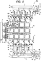
- Fig. 5 is a circuit diagram of an image pickup apparatus according to a second embodiment of the invention.
- Fig. 6 is a timing chart illustrating the operation of the image pickup apparatus shown in Fig. 5.
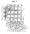
- Fig. 7 is a circuit diagram of an image pickup apparatus according to a third embodiment of the invention.
- Fig. 8 is a timing chart illustrating the operation of the image pickup apparatus shown in Fig. 6.
- Fig. 9 is a circuit diagram of an image pickup apparatus according to a fourth embodiment of the invention.
- Fig. 10 is a timing chart illustrating the operation of the image pickup apparatus shown in Fig. 9.
- Fig. 11 is a diagram showing an image pickup system with an image pickup apparatus, according to a fifth embodiment of the invention.
- Fig. 3 shows a pattern of color filters according to the first embodiment of the invention.
- This pattern has a periodicity of two pixels in the horizontal direction and two pixels in the vertical direction.
- the first row has G and Ye color filters disposed in this order from the left
- the second row has Cy and Mg color filters disposed in this order from the left.
- the pattern of color filters may be reversed right and left, or up and down.
- the luminance signal Y, blue color difference signal CB, and red color difference signal CR can be calculated respectively from the equations (2) and (3) by using Cy, Ye, Mg, and G signals in various color filter patterns.
- Fig. 4 shows a pattern of color filters constituted of a fundamental pattern of two pixels in the horizontal direction and two pixels in the vertical direction. With reference to Fig. 4, particular read methods will be described.
- the color difference signals CB and CR each can be obtained from two pixels in the horizontal direction and two pixels in the vertical direction, resulting in a high resolution.
- the second read method one luminance signal Ye is obtained for every two pixels in the horizontal direction.
- the level of the luminance signal Y is high.
- the luminance signal Y generated by this method is suitable for an autofocus detecting signal particularly when an object has a high horizontal resolution such as a fine vertical stripe pattern and has a low luminance.
- the third read method one luminance signal Ye is obtained for every two pixels in the vertical direction.
- the level of the luminance signal Y is high in the vertical direction.
- the luminance signal Y generated by this method is suitable for an autofocus detecting signal particularly when an object has a high horizontal resolution such as a fine horizontal stripe pattern.
- the fifth read method is suitable for a moving image object.
- An image signal can be read at high speed because the number of read color difference signals of pixels is a half of the first read method.
- Color difference signals CB are calculated by the method similar to the fifth read method.
- the sixth read method is suitable for a moving image object.
- An image signal can be read at high speed because the number of read color difference signals of pixels is a half of the first read method.
- Color difference signals CB are calculated by the method similar to the fifth read method.
- the sixth read method is suitable for a moving image object.
- An image signal can be read at high speed because the number of read color difference signals of pixels is a half of the first read method.
- the color difference signals CB and CR are obtained from the same area.
- the color difference signals CR are calculated by the similar method to the fourth to seventh read methods.
- the eighth to eleventh read methods are suitable for a moving image object.
- An image signal can be read at high speed because the number of read color difference signals of pixels is a half of the first read method.
- the twelfth method is suitable for a moving image object.
- An image signal can be read at high speed because the number of read color difference signals of pixels is a quarter of the first read method.
- the above read methods may be used while pixels are read by thinning them in the unit of a fundamental pattern or a plurality of fundamental pattern to thereby speed up a read operation.
- Fig. 5 is a circuit diagram showing the structure of a CMOS sensor of the second embodiment.
- the CMOS sensor includes: a first output series for outputting a difference between an average value of detection light amounts of two pixels adjacent in the vertical direction in one column and an average value of detection light amounts of two pixels adjacent in the vertical direction in the next column; and a second output series for outputting a difference between an average value of detection light amounts of two pixels adjacent in the horizontal direction in one row and an average value of detection light amounts of two pixels adjacent in the horizontal direction in the next row. Therefore, the CMOS sensor of this embodiment can use the first read method.
- reference numeral 1 represents a vertical scan circuit for generating an enable signal which enables a control signal of each row, the enable signal sequentially becoming active in the vertical direction.
- Reference numeral 100 represents a photodiode serving as a photodetector for converting incidence light into electric charges.
- Reference numeral 101 represents a transfer transistor for transferring the electric charges generated by the photodiode 100 to a floating diffusion region 101 which temporarily stores the transferred electric charges.
- Reference numeral 103 represents a reset transistor for discharging electric charges accumulated in the gate of an amplifier transistor 104.
- Reference numeral 121 represents a switching transistor. The elements 100 to 104, and 121 constitute one pixel.
- Reference numeral 112 represents a constant current source transistor which is activated by a voltage applied to a terminal 7.
- Reference numeral 105 represents a transistor for discharging electric charges in capacitors 109, 110, 117, and 118.
- Reference numeral 106 represents a current distribution division transistor for connecting the source of the transistor 104 to the capacitor 109.
- Reference numeral 107 represents a current distribution transistor for connecting the source of the transistor 104 to the capacitor 110.
- the capacitors 109 and 110 function as a line memory which is charged by a voltage supplied from the transistor 104.
- Reference numeral 108 represents an averaging transistor for averaging the electric charges in the capacitors 109 and 110.
- Reference numeral 111 represents a switching transistor for applying a voltage of the line memory 109 to a buffer 123 at the front stage of a differential amplifier 122 which amplifies a difference between voltages across the capacitors 109 and 109'.
- Reference numeral 113 represents a switching transistor for connecting the source of the transistor 104 to a capacitor 117.
- Reference numeral 114 represents a switching transistor for connecting the source of the transistor 104 to a capacitor 118.
- the capacitors 117 and 118 are charged by a current supplied from the source of the transistor 104.
- Reference numeral 115 represents a switching transistor for controlling to average the electric charges stored in the capacitors 117 and 117'.
- Reference numeral 116 represents a switching transistor for controlling to average the electric charges stored in the capacitors 118 and 118'.
- Reference numeral 119 represents a switching transistor for supplying a voltage of the line memory 117 to a buffer 129 at the front stage of a differential amplifier 127 which amplifies a difference between voltages across the capacitors 117 and 118'.
- the constant current source transistor 112 is activated in the unit of a row, and paired with the transistor 104 to constitute an amplifier.
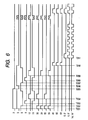
- Fig. 6 is a timing chart illustrating an operation of the CMOS sensor shown in Fig. 5. With reference to Figs. 5 and 6, the operation of the CMOS sensor shown in Fig. 5 will be described.
- a pulse applied to a terminal 11 takes a high state, and pulses applied to M terminals 30, 31, 50, and 51 take the high state. Therefore, the line memories 109, 110, 117, and 118 are reset to initial potentials.
- a start pulse applied to a terminal 2 of the vertical scan circuit 1 and a scan pulse applied to a terminal 3 take the high level, so that the vertical scan circuit 1 starts scanning to select the first row.
- a high level pulse is applied to a terminal 8 to reset the floating diffusion regions of the pixel area.
- a reset pulse at the terminal 8 falls so that the floating diffusion regions of first row pixels are made in an electrically floating state.
- a high level pulse is applied to a terminal 9 so that electric charges are transferred from photodiodes of the first row to the floating diffusion regions.
- a high level pulse is applied to terminals 10, 30, and 50 so that a voltage proportional to light amounts detected with the photodetectors of the first row is read to the capacitors 109 and 117 via the amplifier 104.
- the vertical scan pulse 3 falls.
- the vertical scan pulse 3 again rises to select the second row.
- a reset pulse false so that the floating diffusion regions of pixels of the second row are made in an electrically floating state.
- a high level pulse is applied to the terminal 9 so that electric charges are transferred from photodiodes of the second row to the floating diffusion regions.
- a high level pulse is applied to terminals 10, 30, and 51 so that a voltage proportional to light amounts detected with the photodetectors of the second row is read to the capacitors 110 and 118 via the amplifier 104 of the second row.
- a high level pulse is applied to terminals 40, 60, and 61 to average the electric charges on the line memories.
- a horizontal scan circuit 4 starts scanning so that averaged voltages are sequentially applied in the horizontal direction to the differential amplifiers 122 and 127.
- the differential amplifiers 122 and 127 outputs a blue color difference signal CB and a red color difference signal CR.
- adders made of an operational amplifier or the like to the terminals 70 and 71 and to the terminals 80 and 81, luminance signals can be output.
- an output signal of each pixel in the odd column can be obtained from the output terminal 71, and an output signal of each pixel in the even column can be obtained from the output terminal 70.
- Fig. 7 is a circuit diagram showing the structure of a CMOS sensor of the third embodiment.
- the CMOS sensor includes an output series for outputting an average value of detection light amounts of two pixels adjacent in the horizontal direction or an average of detection light amounts of four pixels adjacent in the horizontal direction. Therefore, the CMOS sensor of this embodiment can use the third read method by summing the two outputs of the CMOS sensor.
- Reference numeral 301 represents a switching transistor for controlling to average electric charges accumulated in capacitors 109 and 109'.
- Reference numeral 302 represents a switching transistor for controlling to average electric charges accumulated in capacitors 110 and 110'.
- Reference numeral 301' represents a switching transistor for controlling to average electric charges accumulated in capacitors 109" and 109"'.
- Reference numeral 302' represents a switching transistor for controlling to average electric charges accumulated in capacitors 110" and 110"'.
- Reference numeral 303 represents a switching transistor for controlling to average electric charges accumulated in the capacitors 109' and 109".
- Reference numeral 304 represents a switching transistor for controlling to average electric charges accumulated in the capacitors 110' and 110". If the switching transistors 301, 301', and 303 are operated synchronously, the electric charges stored in the capacitors 109, 109', 109", and 109"' are averaged. For example, if after or when the switching transistors 301 and 301' are turned on, the switching transistor 303 is turned on, these transistors average the electric charges stored in the capacitors 109, 109', 109", and 109"'. If the switching transistors 302, 302', and 304 are operated synchronously, these transistors average the electric charges stored in the capacitors 110, 110', 110", and 110"'. Namely, if after or when the switching transistors 302 and 304' are turned on, the switching transistor 304 is turned on, these transistors average the electric charges stored in the capacitors 110, 110', 110", and 110"'.
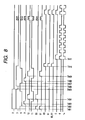
- Fig. 8 is a timing chart illustrating an operation of the CMOS sensor shown in Fig. 7. With reference to Figs. 7 and 8, the operation of the CMOS sensor shown in Fig. 7 will be described.
- a start pulse applied to a terminal 2 of the vertical scan circuit 1 and a scan pulse applied to a terminal 3 take the high level, so that the vertical scan circuit 1 starts scanning to select the first row.
- a high level pulse is applied to a terminal 8 to reset the floating diffusion regions of the pixel area.
- a reset pulse at the terminal 8 falls so that the floating diffusion regions of first row pixels are made in an electrically floating state.
- a high level pulse is applied to a terminal 9 so that electric charges in the photodetectors of the first row are transferred to the floating diffusion regions.
- a high level pulse is applied to terminals 10 and 50 so that a voltage proportional to light amounts detected with the photodetectors of the first row is read to the capacitor 109 via the amplifier 104.
- the vertical scan pulse 3 rises.
- the vertical scan pulse 3 again falls to select the second row.
- a reset pulse false so that the floating diffusion regions of pixels of the second row are made in an electrically floating state.
- a high level pulse is applied to the terminal 9 so that electric charges are transferred from photodiodes of the second row to the floating diffusion regions.
- a high level pulse is applied to terminals 10, and 51 so that a voltage proportional to light amounts detected with the photodetectors of the second row is read to the capacitor 110 via the amplifier 104 of the second row.
- a high level pulse is applied to terminals 60, 61, 90, and 91 to average the electric charges in the capacitors 109, 109', 109", and 109"' on the line memories and to average the electric charges in the capacitors 110, 110', 110", and 110"' on the line memories.
- a horizontal scan circuit 4 starts scanning so that averaged voltages are sequentially output in the horizontal direction. Since a luminance signal is output in this embodiment, only one output terminal 16 is used. If a plurality of output terminals like those shown in Fig. 7 are used, color difference signals can be obtained.
- Fig. 9 is a circuit diagram showing the structure of a CMOS sensor of the fourth embodiment.
- the CMOS sensor includes an output series for outputting an average value of detection light amounts of two pixels adjacent in the vertical direction or an average of detection light amounts of four pixels adjacent in the vertical direction. Therefore, the CMOS sensor of this embodiment can use the second read method by summing the two outputs of the CMOS sensor.
- Reference numerals 501, 502, 503, and 504 represent current distribution transistors for distributing current supplied from a transistor to capacitors 508, 109, 510, and 511.
- the capacitor 508 stores signals from first row photodetectors
- the capacitor 509 stores signals from second row photodetectors
- the capacitor 510 stores signals from third row photodetectors
- the capacitor 511 stores signals from fourth row photodetectors.
- Reference numeral 505 represents a switching transistor for controlling to average electric charges accumulated in the capacitors 508 and 509.
- Reference numeral 506 represents a switching transistor for controlling to average electric charges accumulated in the capacitors 509 and 510.
- Reference numeral 507 represents a switching transistor for controlling to average electric charges accumulated in the capacitors 510 and 511. If the switching transistors 505, 506, and 507 are operated synchronously, the electric charges stored in the capacitors 508, 509, 510, and 511 are averaged. For example, if after or when the switching transistors 505 and 507 are turned on, the switching transistor 506 is turned on, these transistors average the electric charges stored in the capacitors 508, 509, 610, and 511.
- Fig. 10 is a timing chart illustrating an operation of the CMOS sensor shown in Fig. 9. With reference to Figs. 9 and 10, the operation of the CMOS sensor shown in Fig. 9 will be described.
- a start pulse applied to a terminal 2 of the vertical scan circuit 1 and a scan pulse applied to a terminal 3 take the high level, so that the vertical scan circuit 1 starts scanning to select the first row.
- a high level pulse is applied to a terminal 8 to reset the floating diffusion regions of the pixel area.
- a reset pulse at the terminal 8 falls so that the floating diffusion regions of first row pixels are made in an electrically floating state.
- a high level pulse is applied to a terminal 9 so that electric charges in the photodetectors of the first row are transferred to the floating diffusion regions.
- a high level pulse is applied to terminals 10 and 30 so that a voltage proportional to light amounts detected with the photodetectors of the first row is read to the capacitor 508.
- the vertical scan pulse 3 rises.
- the vertical scan pulse 3 again rises to select the second row.
- a reset pulse falls so that the floating diffusion regions of pixels of the second row are made in an electrically floating state.
- a high level pulse is applied to the terminal 9 so that electric charges are transferred from photodiodes of the second row to the floating diffusion regions.
- a high level pulse is applied to terminals 10, and 31 so that a voltage proportional to light amounts detected with the photodetectors of the second row is read to the capacitor 509.
- a high level pulse is applied to terminals 10 and 32 so that a voltage proportional to light amounts detected with the photodetectors of the third row is read to the capacitor 510.
- a high level pulse is applied to terminals 10 and 33 so that a voltage proportional to light amounts detected with the photodetectors of the fourth row is read to the capacitor 511.
- a high level pulse is applied to the terminals 40 and 41 to average the electric charges in the capacitors 508, 509, 510, and 511 on the line memories.
- a horizontal scan circuit 4 starts scanning so that averaged voltages are sequentially output in the horizontal direction. Voltages proportional to average values of light amounts detected with the photodetectors of the first to fourth rows are sequentially output from an output terminal 70.
- an average value of the first and second columns may be output from the output terminal 70 and an average value of the third and fourth columns may be output from an output terminal 71.
- a difference between the average value of the first and second columns and the average value of the third and fourth columns may be output from an output terminal 72.
- a reset voltage at the floating diffusion regions may be read to another line memory, prior to reading image signals of pixels.
- a variation of output voltages to be caused by a variation of threshold voltages of transistors 104 can be eliminated. Therefore, an image signal with a high S/N ratio can be obtained which does not contain noise components to be generated by a variation of image signals caused by a variation of amounts of light detected with photodetectors.
- Vertical/horizontal scanning may be performed by thinning pixels in the unit of one block or a plurality of blocks so that more compressed image signals can be obtained.
- CMOS sensor is used as an example of image pickup elements.
- Other image pickup elements such as CCD and SIT may also be used.
- color filters of four colors including yellow Ye, magenta Mg, cyan Cy, and green G are used.
- Other color filters may also be used if they can obtain a luminance signal and color difference signals.
- Fig. 11 is a block diagram showing the structure of an image pickup system with an image pickup apparatus, according to the fifth embodiment of the invention.
- signals from pixels of an image pickup apparatus 91 such as a CMOS sensor are supplied directly to an A/D converter 92, without processing the signals such as addition calculation to obtain color difference signals and a luminance signal.
- signals After the signals are converted by the A/D converter 92 into digital signals, they are stored in a memory 93.
- a computer 94 performs necessary calculations for digital signals stored in the memory 93 to obtain a luminance signal and color difference signals.
- Software for running the computer 94 may be stored in a storage medium storing programs.
- the storage medium storing such programs may be a floppy disk, a hard disk, an optical disk, a magneto-optical disk, a CD-ROM, a magnetic tape, a semiconductor memory, and a like.
- a color image signal with color difference signals having a high resolution both in the horizontal and vertical directions can be obtained, for example by using the first read method.
- the embodiments can be applied to a multi-mode such as a mode of outputting an image signal at high speed which signal can be used for simple color display, autofocus, white balance adjustment and a mode of outputting an image signal having a high resolution.
Landscapes
- Engineering & Computer Science (AREA)
- Multimedia (AREA)
- Signal Processing (AREA)
- Physics & Mathematics (AREA)
- Spectroscopy & Molecular Physics (AREA)
- Color Television Image Signal Generators (AREA)
Applications Claiming Priority (2)
| Application Number | Priority Date | Filing Date | Title |
|---|---|---|---|
| JP01881398A JP4006075B2 (ja) | 1998-01-30 | 1998-01-30 | Cmosセンサ及び撮像システム |
| JP1881398 | 1998-01-30 |
Publications (3)
| Publication Number | Publication Date |
|---|---|
| EP0933950A2 true EP0933950A2 (de) | 1999-08-04 |
| EP0933950A3 EP0933950A3 (de) | 2000-08-23 |
| EP0933950B1 EP0933950B1 (de) | 2005-12-07 |
Family
ID=11982028
Family Applications (1)
| Application Number | Title | Priority Date | Filing Date |
|---|---|---|---|
| EP99300555A Expired - Lifetime EP0933950B1 (de) | 1998-01-30 | 1999-01-26 | Farbbildaufnahmegerät und -verfahren |
Country Status (6)
| Country | Link |
|---|---|
| US (1) | US7724292B2 (de) |
| EP (1) | EP0933950B1 (de) |
| JP (1) | JP4006075B2 (de) |
| KR (1) | KR100320900B1 (de) |
| CN (1) | CN1122978C (de) |
| DE (1) | DE69928711D1 (de) |
Families Citing this family (17)
| Publication number | Priority date | Publication date | Assignee | Title |
|---|---|---|---|---|
| US7015964B1 (en) | 1998-11-02 | 2006-03-21 | Canon Kabushiki Kaisha | Solid-state image pickup device and method of resetting the same |
| JP3667214B2 (ja) | 2000-08-25 | 2005-07-06 | キヤノン株式会社 | 固体撮像装置およびその駆動方法 |
| JP4154268B2 (ja) | 2003-03-27 | 2008-09-24 | キヤノン株式会社 | 撮像装置 |
| JP4459099B2 (ja) | 2005-03-18 | 2010-04-28 | キヤノン株式会社 | 固体撮像装置及びカメラ |
| US8139130B2 (en) | 2005-07-28 | 2012-03-20 | Omnivision Technologies, Inc. | Image sensor with improved light sensitivity |
| US8274715B2 (en) | 2005-07-28 | 2012-09-25 | Omnivision Technologies, Inc. | Processing color and panchromatic pixels |
| US7916362B2 (en) | 2006-05-22 | 2011-03-29 | Eastman Kodak Company | Image sensor with improved light sensitivity |
| JP4144892B2 (ja) * | 2006-08-28 | 2008-09-03 | キヤノン株式会社 | 光電変換装置及び撮像装置 |
| US8031258B2 (en) | 2006-10-04 | 2011-10-04 | Omnivision Technologies, Inc. | Providing multiple video signals from single sensor |
| US7999870B2 (en) * | 2008-02-01 | 2011-08-16 | Omnivision Technologies, Inc. | Sampling and readout of an image sensor having a sparse color filter array pattern |
| US8385971B2 (en) * | 2008-08-19 | 2013-02-26 | Digimarc Corporation | Methods and systems for content processing |
| JP5675215B2 (ja) * | 2010-08-20 | 2015-02-25 | オリンパス株式会社 | デジタルカメラ |
| US9918017B2 (en) | 2012-09-04 | 2018-03-13 | Duelight Llc | Image sensor apparatus and method for obtaining multiple exposures with zero interframe time |
| KR20150146308A (ko) * | 2014-06-23 | 2015-12-31 | 삼성전자주식회사 | 이미지 센서 및 이미지 센서의 동작 방법 |
| US12401911B2 (en) | 2014-11-07 | 2025-08-26 | Duelight Llc | Systems and methods for generating a high-dynamic range (HDR) pixel stream |
| US12401912B2 (en) | 2014-11-17 | 2025-08-26 | Duelight Llc | System and method for generating a digital image |
| US12445736B2 (en) | 2015-05-01 | 2025-10-14 | Duelight Llc | Systems and methods for generating a digital image |
Family Cites Families (39)
| Publication number | Priority date | Publication date | Assignee | Title |
|---|---|---|---|---|
| GB2014397B (en) | 1978-02-10 | 1982-08-18 | Hitachi Ltd | Solid-state colour imaging device |
| NL7900897A (nl) | 1978-02-15 | 1979-08-17 | Hitachi Ltd | Vaste-stof beeldopneeminrichting. |
| USRE34309E (en) | 1984-12-26 | 1993-07-13 | Canon Kabushiki Kaisha | Image sensor device having plural photoelectric converting elements |
| US4835404A (en) | 1986-09-19 | 1989-05-30 | Canon Kabushiki Kaisha | Photoelectric converting apparatus with a switching circuit and a resetting circuit for reading and resetting a plurality of lines sensors |
| DE3750329D1 (de) | 1986-12-18 | 1994-09-08 | Canon Kk | Signalausleseschaltung. |
| US4879470A (en) | 1987-01-16 | 1989-11-07 | Canon Kabushiki Kaisha | Photoelectric converting apparatus having carrier eliminating means |
| US5583568A (en) * | 1988-08-26 | 1996-12-10 | Canon Kabushiki Kaisha | Solid state image pickup apparatus having improved luminance control |
| US5262870A (en) | 1989-02-10 | 1993-11-16 | Canon Kabushiki Kaisha | Image sensor in which reading and resetting are simultaneously performed |
| US5162912A (en) | 1989-04-10 | 1992-11-10 | Canon Kabushiki Kaisha | Photoelectric conversion apparatus eliminating noise in an output signal |
| ATE181629T1 (de) | 1990-04-23 | 1999-07-15 | Canon Kk | Photoelektrische wandlungsvorrichtung |
| CA2052148A1 (en) | 1990-09-27 | 1992-03-28 | Tadashi Sugiki | Method of driving a solid-state imaging device |
| EP0554035B1 (de) * | 1992-01-27 | 2001-10-17 | Mitsubishi Denki Kabushiki Kaisha | Festkörperfarbbildvideokamera |
| US6952233B2 (en) | 1992-07-23 | 2005-10-04 | Canon Kabushiki Kaisha | Video camera having a material element for controlling light transmission |
| US5541648A (en) | 1992-10-09 | 1996-07-30 | Canon Kabushiki Kaisha | Color image pickup apparatus having a plurality of color filters arranged in an offset sampling structure |
| EP0627847B1 (de) | 1993-05-28 | 2001-04-11 | Canon Kabushiki Kaisha | Photoelektrische Umwandlungsanordnung |
| JPH06339082A (ja) | 1993-05-28 | 1994-12-06 | Canon Inc | 光電変換装置 |
| JP3431995B2 (ja) | 1993-06-03 | 2003-07-28 | キヤノン株式会社 | 撮像装置 |
| JP3571770B2 (ja) | 1994-09-16 | 2004-09-29 | キヤノン株式会社 | 光電変換装置 |
| DE69627559T2 (de) | 1995-02-01 | 2004-01-08 | Canon K.K. | Festkörperbildaufnahmevorrichtung und Betriebsverfahren dazu |
| EP0766480A3 (de) * | 1995-09-28 | 2000-03-01 | Kabushiki Kaisha Toshiba | Festkörper-Farbbildaufnahmegerät |
| US6493025B1 (en) * | 1995-10-05 | 2002-12-10 | Sanyo Electronic Co., Ltd. | Image sensing system equipped with interface between image sensing apparatus and computer machinery |
| JP3755921B2 (ja) | 1996-02-29 | 2006-03-15 | 株式会社コダックデジタルプロダクトセンター | 撮像デバイスのラインノイズ除去方法及びそれを用いたラインノイズ除去装置 |
| US6323901B1 (en) * | 1996-03-29 | 2001-11-27 | Sanyo Electric Co., Ltd. | Single CCD type color camera having high resolution and capable of restricting generation of ghost color |
| JPH09312848A (ja) | 1996-05-21 | 1997-12-02 | Hitachi Ltd | 撮像装置 |
| JP3142239B2 (ja) | 1996-06-11 | 2001-03-07 | キヤノン株式会社 | 固体撮像装置 |
| JP3707187B2 (ja) | 1996-09-18 | 2005-10-19 | コニカミノルタホールディングス株式会社 | 電子カメラ |
| JP3649841B2 (ja) | 1997-02-20 | 2005-05-18 | 三洋電機株式会社 | 単板式カラーカメラ |
| US6002287A (en) | 1997-05-08 | 1999-12-14 | Canon Kabushiki Kaisha | Signal outputting apparatus |
| JP3673620B2 (ja) | 1997-07-18 | 2005-07-20 | キヤノン株式会社 | 光電変換装置 |
| JP3466886B2 (ja) | 1997-10-06 | 2003-11-17 | キヤノン株式会社 | 固体撮像装置 |
| JP3556447B2 (ja) | 1997-11-07 | 2004-08-18 | シャープ株式会社 | カラー固体撮像カメラシステム |
| US6559886B1 (en) | 1997-12-04 | 2003-05-06 | Victor Company Of Japan, Limited | Video signal processing method and device |
| JP3496918B2 (ja) | 1997-12-26 | 2004-02-16 | キヤノン株式会社 | 固体撮像装置 |
| JPH11196427A (ja) * | 1997-12-26 | 1999-07-21 | Canon Inc | 単板カラー撮像装置 |
| JP4377976B2 (ja) | 1997-12-26 | 2009-12-02 | キヤノン株式会社 | カラー撮像装置、画像信号読み出し方法、画像処理装置、画像処理システム、及び記憶媒体 |
| US6330029B1 (en) * | 1998-03-17 | 2001-12-11 | Eastman Kodak Company | Particular pattern of pixels for a color filter array which is used to derive luminance and chrominance values |
| US6963372B1 (en) | 1998-04-24 | 2005-11-08 | Canon Kabushiki Kaisha | Solid-state image sensing apparatus and method of operating the same |
| US6529239B1 (en) | 1998-06-01 | 2003-03-04 | Fairchild Imaging, Inc. | Image sensor with stripes of cyan filter material perpendicular to stripes of yellow filter material |
| US6992714B1 (en) * | 1999-05-31 | 2006-01-31 | Canon Kabushiki Kaisha | Image pickup apparatus having plural pixels arranged two-dimensionally, and selective addition of different pixel color signals to control spatial color arrangement |
-
1998
- 1998-01-30 JP JP01881398A patent/JP4006075B2/ja not_active Expired - Fee Related
-
1999
- 1999-01-26 EP EP99300555A patent/EP0933950B1/de not_active Expired - Lifetime
- 1999-01-26 DE DE69928711T patent/DE69928711D1/de not_active Expired - Lifetime
- 1999-01-29 CN CN99100436A patent/CN1122978C/zh not_active Expired - Fee Related
- 1999-01-29 KR KR1019990003000A patent/KR100320900B1/ko not_active Expired - Fee Related
-
2006
- 2006-06-23 US US11/473,024 patent/US7724292B2/en not_active Expired - Fee Related
Also Published As
| Publication number | Publication date |
|---|---|
| CN1122978C (zh) | 2003-10-01 |
| US20070013796A1 (en) | 2007-01-18 |
| EP0933950B1 (de) | 2005-12-07 |
| KR100320900B1 (ko) | 2002-02-04 |
| EP0933950A3 (de) | 2000-08-23 |
| US7724292B2 (en) | 2010-05-25 |
| KR19990068222A (ko) | 1999-08-25 |
| JPH11220740A (ja) | 1999-08-10 |
| DE69928711D1 (de) | 2006-01-12 |
| CN1234579A (zh) | 1999-11-10 |
| JP4006075B2 (ja) | 2007-11-14 |
Similar Documents
| Publication | Publication Date | Title |
|---|---|---|
| EP0933950A2 (de) | Farbbildaufnahmegerät | |
| KR100307471B1 (ko) | 촬상장치,화상신호판독방법및화상신호처리시스템 | |
| US6784928B1 (en) | Solid state image pickup device and signal reading method thereof | |
| JP6239975B2 (ja) | 固体撮像装置及びそれを用いた撮像システム | |
| US8023018B2 (en) | Drive method for solid-state imaging device, solid-state imaging device, and imaging apparatus | |
| US20070126900A1 (en) | Solid-state image-sensing device that compensates for brightness at edges of a display area and a driving method thereof | |
| CN105763819B (zh) | 图像传感器和摄像设备 | |
| US20100149393A1 (en) | Increasing the resolution of color sub-pixel arrays | |
| US20090027530A1 (en) | Solid-state image pick-up device | |
| US7710483B2 (en) | Solid-state imaging apparatus, driving method thereof, and camera | |
| JP2011024222A (ja) | センサ回路の列回路における画素信号のビニングおよび補間 | |
| CN110231693A (zh) | 图像传感器 | |
| JP2021176211A (ja) | 光電変換装置及び光電変換システム | |
| RU2378791C2 (ru) | Устройство для восприятия изображений и система для захвата изображений | |
| JPH11191892A (ja) | 画像信号処理装置 | |
| JPH09238355A (ja) | 撮像デバイスのラインノイズ除去方法及びそれを用いたラインノイズ除去装置 | |
| JP6508805B2 (ja) | 撮像素子および撮像装置 | |
| JP4262290B2 (ja) | 撮像素子、画像処理装置、画像処理システム、及び記憶媒体 | |
| JPS6016155B2 (ja) | 色彩信号発生装置 | |
| JP3459538B2 (ja) | 単板式カラーカメラの色信号処理回路 | |
| JPH0528037B2 (de) | ||
| JP2940820B2 (ja) | 単板式カラーカメラおよび色信号の分離方法 | |
| JPS60263592A (ja) | 固体撮像装置 | |
| JP4055051B2 (ja) | 固体撮像装置及び固体撮像装置の駆動方法 | |
| JPS62104290A (ja) | 撮像装置 |
Legal Events
| Date | Code | Title | Description |
|---|---|---|---|
| PUAI | Public reference made under article 153(3) epc to a published international application that has entered the european phase |
Free format text: ORIGINAL CODE: 0009012 |
|
| AK | Designated contracting states |
Kind code of ref document: A2 Designated state(s): DE FR GB IT NL |
|
| AX | Request for extension of the european patent |
Free format text: AL;LT;LV;MK;RO;SI |
|
| PUAL | Search report despatched |
Free format text: ORIGINAL CODE: 0009013 |
|
| AK | Designated contracting states |
Kind code of ref document: A3 Designated state(s): AT BE CH CY DE DK ES FI FR GB GR IE IT LI LU MC NL PT SE |
|
| AX | Request for extension of the european patent |
Free format text: AL;LT;LV;MK;RO;SI |
|
| 17P | Request for examination filed |
Effective date: 20010123 |
|
| AKX | Designation fees paid |
Free format text: DE FR GB IT NL |
|
| 17Q | First examination report despatched |
Effective date: 20030826 |
|
| GRAP | Despatch of communication of intention to grant a patent |
Free format text: ORIGINAL CODE: EPIDOSNIGR1 |
|
| RTI1 | Title (correction) |
Free format text: COLOUR IMAGE PICKUP APPARATUS AND METHOD |
|
| GRAS | Grant fee paid |
Free format text: ORIGINAL CODE: EPIDOSNIGR3 |
|
| GRAA | (expected) grant |
Free format text: ORIGINAL CODE: 0009210 |
|
| AK | Designated contracting states |
Kind code of ref document: B1 Designated state(s): DE FR GB IT NL |
|
| PG25 | Lapsed in a contracting state [announced via postgrant information from national office to epo] |
Ref country code: NL Free format text: LAPSE BECAUSE OF FAILURE TO SUBMIT A TRANSLATION OF THE DESCRIPTION OR TO PAY THE FEE WITHIN THE PRESCRIBED TIME-LIMIT Effective date: 20051207 Ref country code: IT Free format text: LAPSE BECAUSE OF FAILURE TO SUBMIT A TRANSLATION OF THE DESCRIPTION OR TO PAY THE FEE WITHIN THE PRESCRIBED TIME-LIMIT;WARNING: LAPSES OF ITALIAN PATENTS WITH EFFECTIVE DATE BEFORE 2007 MAY HAVE OCCURRED AT ANY TIME BEFORE 2007. THE CORRECT EFFECTIVE DATE MAY BE DIFFERENT FROM THE ONE RECORDED. Effective date: 20051207 |
|
| REG | Reference to a national code |
Ref country code: GB Ref legal event code: FG4D |
|
| REF | Corresponds to: |
Ref document number: 69928711 Country of ref document: DE Date of ref document: 20060112 Kind code of ref document: P |
|
| PG25 | Lapsed in a contracting state [announced via postgrant information from national office to epo] |
Ref country code: DE Free format text: LAPSE BECAUSE OF FAILURE TO SUBMIT A TRANSLATION OF THE DESCRIPTION OR TO PAY THE FEE WITHIN THE PRESCRIBED TIME-LIMIT Effective date: 20060308 |
|
| NLV1 | Nl: lapsed or annulled due to failure to fulfill the requirements of art. 29p and 29m of the patents act | ||
| PLBE | No opposition filed within time limit |
Free format text: ORIGINAL CODE: 0009261 |
|
| STAA | Information on the status of an ep patent application or granted ep patent |
Free format text: STATUS: NO OPPOSITION FILED WITHIN TIME LIMIT |
|
| 26N | No opposition filed |
Effective date: 20060908 |
|
| EN | Fr: translation not filed | ||
| PG25 | Lapsed in a contracting state [announced via postgrant information from national office to epo] |
Ref country code: FR Free format text: LAPSE BECAUSE OF FAILURE TO SUBMIT A TRANSLATION OF THE DESCRIPTION OR TO PAY THE FEE WITHIN THE PRESCRIBED TIME-LIMIT Effective date: 20070126 |
|
| PG25 | Lapsed in a contracting state [announced via postgrant information from national office to epo] |
Ref country code: FR Free format text: LAPSE BECAUSE OF FAILURE TO SUBMIT A TRANSLATION OF THE DESCRIPTION OR TO PAY THE FEE WITHIN THE PRESCRIBED TIME-LIMIT Effective date: 20060131 |
|
| PG25 | Lapsed in a contracting state [announced via postgrant information from national office to epo] |
Ref country code: FR Free format text: LAPSE BECAUSE OF FAILURE TO SUBMIT A TRANSLATION OF THE DESCRIPTION OR TO PAY THE FEE WITHIN THE PRESCRIBED TIME-LIMIT Effective date: 20051207 |
|
| PGFP | Annual fee paid to national office [announced via postgrant information from national office to epo] |
Ref country code: GB Payment date: 20140123 Year of fee payment: 16 |
|
| GBPC | Gb: european patent ceased through non-payment of renewal fee |
Effective date: 20150126 |
|
| PG25 | Lapsed in a contracting state [announced via postgrant information from national office to epo] |
Ref country code: GB Free format text: LAPSE BECAUSE OF NON-PAYMENT OF DUE FEES Effective date: 20150126 |