EP0916159B1 - Statische speicherzelle - Google Patents
Statische speicherzelle Download PDFInfo
- Publication number
- EP0916159B1 EP0916159B1 EP97938082A EP97938082A EP0916159B1 EP 0916159 B1 EP0916159 B1 EP 0916159B1 EP 97938082 A EP97938082 A EP 97938082A EP 97938082 A EP97938082 A EP 97938082A EP 0916159 B1 EP0916159 B1 EP 0916159B1
- Authority
- EP
- European Patent Office
- Prior art keywords
- transistor
- source
- drain
- pulldown
- pulldown transistor
- Prior art date
- Legal status (The legal status is an assumption and is not a legal conclusion. Google has not performed a legal analysis and makes no representation as to the accuracy of the status listed.)
- Expired - Lifetime
Links
Images



Classifications
-
- H—ELECTRICITY
- H10—SEMICONDUCTOR DEVICES; ELECTRIC SOLID-STATE DEVICES NOT OTHERWISE PROVIDED FOR
- H10B—ELECTRONIC MEMORY DEVICES
- H10B10/00—Static random access memory [SRAM] devices
-
- H—ELECTRICITY
- H10—SEMICONDUCTOR DEVICES; ELECTRIC SOLID-STATE DEVICES NOT OTHERWISE PROVIDED FOR
- H10B—ELECTRONIC MEMORY DEVICES
- H10B99/00—Subject matter not provided for in other groups of this subclass
Definitions
- the present invention relates generally to memory devices and in particular the present invention relates to a memory device having static memory cells fabricated with a single bit line.
- Static random access memories comprise static memory cells which are designed to operate as a data latch.
- the memory cells typically use access transistors to couple the memory cell to a pair of complementary bit lines.
- the memory cell access transistors arc selectively activated using a word line signal.
- Sense amplifier circuitry is used to detect voltage differentials between the bit lines.
- a pair of cross-coupled pulldown transistors are typically connected to the access transistors and are used to latch data.
- EP-A- 0 087 979 describes a SRAM A balanced SRAM cell comprising:
- the SRAM according to the present invention is characterised in that the drain and source of the first access transistor and the drain and source of the first pulldown transistor are aligned; and the drain and source of the second access transistor and the drain and source of the second pulldown transistor are aligned, with the sources of the pulldown transistors located at one end; and the second layer of polysilicon crosses over the first layer of polysilicon.
- the present invention provides a method of fabricating an SRAM cell comprising:
- a static memory cell which has a single, word line and un-interrupted active area.
- the present invention describes a static memory cell comprising access transistors coupled to bit lines, each of the access transistors having a gate connected to a single word line, and pulldown transistors connected to the access transistors.
- Each of the pulldown transistors has a gate fabricated essentially parallel to the single word line in a plan view.
- An SRAM cell which comprises a first access transistor having a drain connected to a first bit line and a gate connected to a single word line.
- the cell includes a first pulldown transistor having a drain connected to a source of the first access transistor, a source coupled to a bias voltage, and a gate fabricated parallel to the single word line in a plan view.
- a second access transistor is provided which has a drain connected to a second bit line and a gate connected to the single word line.
- a second pulldown transistor is provided which has a drain connected to a source of the second access transistor, a source coupled to the bias voltage, and a gate fabricated parallel to the single word line in a plan view.
- a static random access memory device which comprises an array of static memory cells.
- the static memory cells comprise a first access transistor connected to a first pulldown transistor thereby defining a first current path, and a second access transistor connected to a second pulldown transistor thereby defining a second current path substantially equal to the first current path.
- the memory has a plurality of data communication paths for bi-directional data communication with an external processor, and an address decoder for decoding an address signal provided by the external processor and accessing the array.
- an SRAM cell which comprises a first access transistor fabricated in a first silicon active area having a drain connected to a first bit line, and a gate connected to a single word line.
- a first pulldown transistor is fabricated in the first silicon active area having a drain connected to a source of the first access transistor, and a source coupled to a bias voltage thereby defining a first electrical current path through the first silicon active area.
- a second access transistor fabricated in a second silicon active area having a drain connected to a second bit line, and a gate connected to the single word line.
- a second pulldown transistor fabricated in the second silicon active area having a drain connected to a source of the second access transistor, and a source coupled to the bias voltage thereby defining a second electrical path through the second silicon active area which is substantially symmetrical with first electrical current path.
- the basic static memory 10 is well known in the art to include a memory array 12 constructed of rows and columns of static memory cells having inputs and outputs corresponding to rows and columns.
- Row decode circuit 14 and column 16 decode circuitry is provided to access the memory array in response to an address provided by an external controller 20, such as a standard microprocessor.
- Control circuitry 18 is provided to control either synchronous or asynchronous data communication between the memory 10 and external devices. Buffers are coupled to the data communication lines (DQ's) for bi-directional data communication with the memory array 12.
- DQ's data communication lines
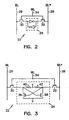
- FIG 2 illustrates a functional diagram of a static memory cell 22.
- the memory cells operate as a data latch 24 which can be connected to complementary bit lines 26 and 28 by activating access transistors 30 and 32 using a common word line 34.
- the static memory cell can be fabricated as shown in Figure 3 having two cross coupled pulldown transistors 36 and 38.
- the access transistors 30 and 32 are activated by providing a signal on the word line 34. Voltages provided on the complimentary bit lines 26 and 28 are sufficient to place the latch in a state corresponding to the bit lines. If the memory cell was storing data of an opposite logic state, the bit line voltages toggle the latch 24 by overpowering bias currents through pull-up resistors 40 and 42.
- bit line 26 is at a high potential and bit line 28 is at a low potential when the word line transitions to a high potential
- transistor 38 is activated and transistor 36 is turned off.
- the access transistors are activated to couple the pulldown transistors 36 and 38 to bit lines 26 and 28.
- Sense amplifier circuitry (not shown) is provided to detect and amplify a differential voltage provided on the bit lines. It will be understood that the SRAM 10 is fabricated as an integrated circuit and that a minimum memory cell layout is desired to maximize memory density.
- FIG. 4 An example of this SRAM memory cell design is shown in the plan view of Figure 4.
- the memory cell has two access transistors fabricated using active areas 50 and 52. Each access transistor has a drain region connected to a bit line (not shown) through bit line contacts 54 and 55. The gate of each access transistor is connected to a word line 56 fabricated with a first layer of polysilicon (poly 1). One pulldown transistor is fabricated using active area 53. A second pulldown transistor is fabricated using active area 52. The gates 58 and 60 of both pulldown transistors are fabricated in poly 1. It is apparent from Figure 4 that in a plan view the gates are fabricated at a diagonal with the word line.
- the second pulldown transistor gates current from VSS (ground) to the source of the second access transistor.
- VSS ground
- bit line contact 55 all of the current from VSS to the access transistor, and to bit line contact 55, is carried through active area.
- the active area of the first pulldown transistor is separated from active area 50, its drain is connected to a buried contact 62.
- the buried contact is connected to area 64 of the poly 1 layer defining the gate 58 of the second pulldown transistor.
- the polysilicon gate 58 connects the two separate active areas 50 and 53 which carries the first pulldown transistor's current to through an exhumed contact 66 where it can then be passed through the access transistor to the bit line contact 54.
- the exhumed contact 66 connects poly I layer 58 to active area 50 through a second layer of poly 67. It will be appreciated that pullup devices, such as resistors 40 and 42 or thin film transistors (TFT), are included in the SRAM cell (not shown) and are fabricated over the pulldown devices.
- pullup devices such as resistors 40 and 42 or thin film transistors (TFT) are included in the SRAM cell (not shown) and are fabricated over the pulldown devices.
- a dual word line SRAM memory cell As an alternative to the above described SRAM memory cell, a dual word line SRAM memory cell was introduced. Referring to the plan view of Figure 5, the dual (or split) word line memory cell is fabricated symmetrically such that two pulldown transistors are substantially identical. In this memory, the word line is split into two separate word lines 66 and 68 which carry the same signal. Uninterrupted active area can be used to connect the two bit line contact areas 70 and 72 to VSS.
- a first access transistor is defined by active area region 73 and active area region 74.
- the first word line 66 is fabricated in a poly 1 layer.
- a first pulldown transistor is defined by active areas 74 and 76.
- the gate 80 of the pulldown transistor is fabricated in a poly 1 layer.
- the second access transistor is defined by active area region 77 and active area region 78.
- the second word line 68 is fabricated in a poly 1 layer.
- a second pulldown transistor is defined by active areas 78 and 82.
- the gate 84 of the second pulldown transistor is fabricated in the poly 1 layer.
- Figure 6 is a plan view of a single digit line SRAM memory cell of the present invention fabricated such that current flows from VSS to bit line contacts entirely in active area.
- the gates of both pulldown transistors are fabricated essentially parallel to the common word line.
- a static memory cell which has a first access transistor fabricated using active area regions 100 and 102 as drain and source regions, respectively.
- a polysilicon gate is fabricated as a common word line 112 which also forms a gate for a second access transistor.
- the second access transistor is defined by drain and source regions 106 and 108, respectively, formed using continuous active area.
- the source of each access transistor is integrally connected to a pulldown transistor.
- the source of the first access transistor is connected to the drain of a first pulldown transistor defined by active area 102 which acts as a drain region, active area 104 which operates as a source region, and a polysilicon gate 114.
- the source of the second access transistor is connected to the drain of a second pulldown transistor defined by active area 108 which acts as a drain region, active area 110 which operates as a source region, and a polysilicon gate 116.
- the source region of each pulldown transistor is connected to a supply voltage, preferably VSS. It will be appreciated that in these described embodiments, an SRAM cell using such devices for pulldown and access devices may just as easily be constructed using p-channel devices where Vcc is substituted for Vss and the polarities of signals are reversed.
- the pulldown transistor drain 102 is connected to the gate poly 116 of the second pulldown transistor through a second polysilicon layer 118 and two contacts.
- the second layer of polysilicon 118 is connected to the active area region 102 through a self-aligned contact 120, as known to those skilled in the art.
- the gate 116 is connected to second polysilicon layer 118 through a cell contact 122.
- the second pulldown transistor drain 108 is connected to the gate 114 of the first pulldown transistor through a slightly larger second polysilicon layer 124 and a cell contact 126.
- second polysilicon layer 124 is connected to active area 108 through a self-aligned contact 128.
- Self-aligned contacts 130 are preferably used to connect active areas 100 and 106 to second layers of polysilicon 132 which can be connected to complementary bit lines (not shown) through their use as landing pads for subsequently formed bit line contacts.
- An optional polysilicon second layer 134 is provided to strap the VSS active area connected to the source regions of the pulldown transistors. It will be appreciated by those skilled in the art that active area regions 100, 102, 104, 106, 108 and 110 are formed from a single uninterrupted active area which has regions of doped silicon. These continuous active areas can be more easily seen in Figures 7 and 8, as explained below.
- the active area is aligned in strips to reduce two-dimensional encroachment corners which exist in the prior single bit line memory cell.
- Cross coupling of the pulldown transistor gates to the other pulldown transistor's drain is done using cell contacts and a second level of interconnect poly.
- This interconnect poly does not carry any appreciable current since it is only used to charge up the pulldown gates. Therefore, variability in the internal contact's resistance does not cause cell stability failure.
- the use of a single word line greatly reduces the area required for the cell while still enabling a very symmetrical cell (in terms of device characteristics versus misalignment). This is due to the elimination of the internal cell contacts that carry current from VSS to the bit lines.
- Figure 7 is a simplified cross section of the memory cell of Figure 6 along line 7-7. It can be seen that a single active area 140 connects the source region 104 of the first pulldown transistor to the self-aligned contact 130 which is coupled to the bit line poly contact area 132. Region 102 is connected to the second pulldown transistor gate 116 through contact 120, poly layer 118 and cell contact 122.
- Figure 8 is a simplified cross section of the memory cell of Figure 6 along line 8-8.
- the single active area 142 connects the source region 110 of the second pulldown transistor to the self-aligned contact 130 which is coupled to the bit line poly contact area 132.
- Region 108 is connected to the first pulldown transistor gate 114 through contact 128, poly layer 124 and cell contact 126.
- FIGs 7 and 8 are simplified cross sections which are intended to illustrate one possible fabrication of the memory of the present invention. Other types of elements can be substituted for those described to achieve the desired result. For example, other contacts known to those skilled in the art can be used in place of self-aligned contacts 130.
- the cell described minimizes area on the memory chip by forming the pulldown gates parallel to the wordlines.
- the space between adjacent cell pulldown transistors provides the active area path from Vss to the access device sources.
- no arrangement of poly/active area patterns could provide a smaller area requirement.
- the size of the cell is limited by the active area and poly patterns.
- a single bit line static memory cell has been described which has two pulldown transistors coupled to access transistors. Each pulldown transistor is fabricated such that a current path between bit line contacts and a reference potential is provided through a continuous active area region. In a plan view, the memory cell has pulldown transistor gates fabricated parallel to a common word line.
Landscapes
- Semiconductor Memories (AREA)
- Static Random-Access Memory (AREA)
Claims (9)
- Ausgeglichene SRAM-Zelle, aufweisend:einen ersten Zugriffstransistor mit einer mit einer ersten Bitleitung verbundenen Drain-Elektrode (100) und einer mit einer einzigen Wortleitung (112) verbundenen Gate-Elektrode,einen ersten Pulldown-Transistor mit einer mit einer Source-Elektrode des ersten Zugriffstransistors verbundenen Drain-Elektrode (102), einer Source-Elektrode (104) zum Empfang einer Vorspannung und einer in Aufsicht parallel zur einzigen Wortleitung (112) hergestellten Gate-Elektrode (114),einen zweiten Zugriffstransistor mit einer mit einer zweiten Bitleitung verbundenen Drain-Elektrode (106) und einer mit der einzigen Wortleitung (112) verbundenen Gate-Elektrode undeinen zweiten Pulldown-Transistor mit einer mit einer Source-Elektrode des zweiten Zugriffstransistors verbundenen Drain-Elektrode (108), einer mit der Source-Elektrode (104) des ersten Pulldown-Transistors verbundenen Source-Elektrode (110) und einer in Aufsicht parallel zur einzigen Wortleitung (112) hergestellten Gate-Elektrode (116), wobei der erste und der zweite Pulldown-Transistor auf der gleichen Seite der einzigen Wortleitung (112) angeordnet sind und die Transistoren in einem einzigen ununterbrochenen aktiven Bereich ausgebildet sind,eine erste Schicht (116) aus Polysilizium, die die Gate-Elektrode des zweiten Pulldown-Transistors bildet und mit der Drain-Elektrode (102) des ersten Pulldown-Transistors verbunden ist, undeine zweite Schicht (124) aus Polysilizium, die die Gate-Elektrode (114) des ersten Pulldown-Transistors mit der Drain-Elektrode (108) des zweiten Pulldown-Transistors verbindet,dadurch gekennzeichnet, daß die Drain- und die Source-Elektrode (100, 102) des ersten Zugriffstransistors und die Drain- und die Source-Elektrode (102, 104) des ersten Pulldown-Transistors aufeinander ausgerichtet sind und die Drain- und die Source-Elektrode (106, 108) des zweiten Zugriffstransistors und die Drain- und die Source-Elektrode (108, 110) des zweiten Pulldown-Transistors aufeinander ausgerichtet sind, wobei die Source-Elektroden (104, 110) der Pulldown-Transistoren an einem Ende des aktiven Bereichs angeordnet sind, und
die zweite Schicht (124) aus Polysilizium die erste Schicht (116) aus Polysilizium überquert. - SRAM-Zelle nach Anspruch 1, wobei der erste Pulldown-Transistor und der erste Zugriffstransistor einen ersten Strompfad bilden und der zweite Pulldown-Transistor und der zweite Zugriffstransistor einen zweiten Strompfad bilden, der dem ersten Strompfad im wesentlichen gleicht.
- SRAM-Zelle nach Anspruch 1, wobei die einzige Wortleitung (112) in einer Polysilizium-Schicht hergestellt ist.
- SRAM-Zelle nach Anspruch 1, wobei die Gate-Elektrode (114) des ersten Pulldown-Transistors in einer Polysilizium-Schicht hergestellt ist.
- SRAM-Zelle nach Anspruch 1, weiterhin aufweisend:eine mit dem ersten Pulldown-Transistor verbundene erste Pullup-Einrichtung undeine mit dem zweiten Pulldown-Transistor verbundene zweite Pullup-Einrichtung.
- SRAM-Zelle nach Anspruch 5, wobei die erste und die zweite Pullup-Einrichtung Dünnfilmtransistoren sind.
- SRAM-Zelle nach Anspruch 1, die in einer Speichereinrichtung vorgesehen ist, die folgendes aufweist:mehrere Datenkommunikationswege zur bidirektionalen Datenkommunikation mit einem externen Prozessor undeinen Adressdekoder zum Dekodieren eines von dem externen Prozessor gelieferten Adressignals und zum Zugriff auf ein Feld.
- SRAM-Zelle nach Anspruch 1, weiterhin aufweisend:einen ersten und einen zweiten selbstausgerichteten Kontakt (120, 128), die in Nachbarschaft der einzigen Wortleitung (112) hergestellt sind und von denen der erste selbstausgerichtete Kontakt (120) einen Kontakt zu einer Source-Elektrode des ersten Zugriffstransistors herstellt und der zweite selbstausgerichtete Kontakt (128) einen Kontakt zu einer Source-Elektrode des zweiten Zugriffstransistors herstellt.
- Verfahren zur Herstellung einer SRAM-Zelle, wobei
eine einzige Wortleitung (112) hergestellt wird,
ein erster Zugriffstransistor und ein erster Pulldown-Transistor hergestellt werden, wobei der erste Zugriffstransistor eine Drain-Elektrode (100) und eine Source-Elektrode (102) und der erste Pulldown-Transistor eine mit der Source-Elektrode (102) des ersten Zugriffstransistors verbundene Drain-Elektrode (102), eine Source-Elektrode (104) zum Empfang einer Vorspannung und eine in Aufsicht parallel zur einzigen Wortleitung (112) hergestellte Gate-Elektrode (114) aufweist, wobei die Drain- und die Source-Elektrode (100, 102) des ersten Zugriffstransistors und die Drain- und die Source-Elektrode (102, 104) des ersten Pulldown-Transistors in einem ersten Streifen eines einzigen ununterbrochenen Bereichs ausgebildet sind, und
ein zweiter Zugriffstransistor und ein zweiter Pulldown-Transistor hergestellt werden, von denen der zweite Zugriffstransistor eine Drain-Elektrode (106) und eine Source-Elektrode (108) und der zweite Pulldown-Transistor eine mit der Source-Elektrode (108) des zweiten Zugriffstransistors verbundene Drain-Elektrode (108), eine mit der Source-Elektrode (104) des ersten Pulldown-Transistors verbundene Source-Elektrode (110) und eine in Aufsicht parallel zur einzigen Wortleitung (112) hergestellte Gate-Elektrode (116) aufweist, wobei die Drain- und die Source-Elektrode (106, 108) des zweiten Zugriffstransistors und die Drain- und die Source-Elektrode (108, 110) des zweiten Pulldown-Transistors in einem zweiten Streifen eines einzigen ununterbrochenen Bereichs ausgebildet sind und wobei der erste und der zweite Pulldown-Transistor auf der gleichen Seite der einzigen Wortleitung (112) angeordnet sind,
eine erste Schicht (116) aus Polysilizium hergestellt wird, die die Gate-Elektrode des zweiten Pulldown-Transistors bildet und mit der Drain-Elektrode (102) des ersten Pulldown-Transistors verbunden ist, und
eine zweite Schicht (124) aus Polysilizium hergestellt wird, die die Gate-Elektrode (114) des ersten Pulldown-Transistors mit der Drain-Elektrode (108) des zweiten Pulldown-Transistors verbindet,
dadurch gekennzeichnet, daß die Drain- und die Source-Elektrode (100, 102) des ersten Zugriffstransistors und die Drain- und die Source-Elektrode (102, 104) des ersten Pulldown-Transistors aufeinander ausgerichtet sind und die Drain- und die Source-Elektrode (106, 108) des zweiten Zugriffstransistors und die Drain- und die Source-Elektrode (108, 110) des zweiten Pulldown-Transistors aufeinander ausgerichtet sind, wobei die Source-Elektroden (104, 110) der Pulldown-Transistoren an einem Ende des aktiven Bereichs angeordnet sind, und
die zweite Schicht (124) aus Polysilizium die erste Schicht (116) aus Polysilizium überquerst.
Applications Claiming Priority (3)
| Application Number | Priority Date | Filing Date | Title |
|---|---|---|---|
| US690124 | 1996-07-31 | ||
| US08/690,124 US5818750A (en) | 1996-07-31 | 1996-07-31 | Static memory cell |
| PCT/US1997/013498 WO1998005070A1 (en) | 1996-07-31 | 1997-07-31 | Static memory cell |
Publications (2)
| Publication Number | Publication Date |
|---|---|
| EP0916159A1 EP0916159A1 (de) | 1999-05-19 |
| EP0916159B1 true EP0916159B1 (de) | 2005-09-21 |
Family
ID=24771200
Family Applications (1)
| Application Number | Title | Priority Date | Filing Date |
|---|---|---|---|
| EP97938082A Expired - Lifetime EP0916159B1 (de) | 1996-07-31 | 1997-07-31 | Statische speicherzelle |
Country Status (7)
| Country | Link |
|---|---|
| US (4) | US5818750A (de) |
| EP (1) | EP0916159B1 (de) |
| KR (2) | KR100734982B1 (de) |
| AT (1) | ATE305173T1 (de) |
| AU (1) | AU4049197A (de) |
| DE (1) | DE69734241T2 (de) |
| WO (1) | WO1998005070A1 (de) |
Cited By (1)
| Publication number | Priority date | Publication date | Assignee | Title |
|---|---|---|---|---|
| TWI427639B (zh) * | 2006-05-31 | 2014-02-21 | Advanced Risc Mach Ltd | 記憶體單元中之金屬線佈局 |
Families Citing this family (21)
| Publication number | Priority date | Publication date | Assignee | Title |
|---|---|---|---|---|
| US5818750A (en) * | 1996-07-31 | 1998-10-06 | Micron Technology, Inc. | Static memory cell |
| US6174764B1 (en) | 1997-05-12 | 2001-01-16 | Micron Technology, Inc. | Process for manufacturing integrated circuit SRAM |
| US6226748B1 (en) | 1997-06-12 | 2001-05-01 | Vpnet Technologies, Inc. | Architecture for virtual private networks |
| US6301696B1 (en) | 1999-03-30 | 2001-10-09 | Actel Corporation | Final design method of a programmable logic device that is based on an initial design that consists of a partial underlying physical template |
| US6446242B1 (en) | 1999-04-02 | 2002-09-03 | Actel Corporation | Method and apparatus for storing a validation number in a field-programmable gate array |
| US6211697B1 (en) | 1999-05-25 | 2001-04-03 | Actel | Integrated circuit that includes a field-programmable gate array and a hard gate array having the same underlying structure |
| US6295224B1 (en) | 1999-12-30 | 2001-09-25 | Stmicroelectronics, Inc. | Circuit and method of fabricating a memory cell for a static random access memory |
| US20020055190A1 (en) * | 2000-01-27 | 2002-05-09 | Anthony Thomas C. | Magnetic memory with structures that prevent disruptions to magnetization in sense layer |
| US6937063B1 (en) | 2000-09-02 | 2005-08-30 | Actel Corporation | Method and apparatus of memory clearing with monitoring RAM memory cells in a field programmable gated array |
| US7029963B2 (en) * | 2001-08-30 | 2006-04-18 | Micron Technology, Inc. | Semiconductor damascene trench and methods thereof |
| TW522526B (en) * | 2002-01-31 | 2003-03-01 | Brilliance Semiconductor Inc | Method for improving the SRAM cell stability |
| US20030217223A1 (en) * | 2002-05-14 | 2003-11-20 | Infineon Technologies North America Corp. | Combined command set |
| US20030214847A1 (en) * | 2002-05-14 | 2003-11-20 | Infineon Technologies North America Corp. | Wordline pulldown circuit |
| US6879507B2 (en) * | 2002-08-08 | 2005-04-12 | Micron Technology, Inc. | Conductive structure for microelectronic devices and methods of fabricating such structures |
| US6864712B2 (en) * | 2003-04-28 | 2005-03-08 | Stmicroelectronics Limited | Hardening logic devices |
| US9236383B2 (en) * | 2004-04-27 | 2016-01-12 | Micron Technology, Inc. | Method and apparatus for fabricating a memory device with a dielectric etch stop layer |
| US7141511B2 (en) * | 2004-04-27 | 2006-11-28 | Micron Technology Inc. | Method and apparatus for fabricating a memory device with a dielectric etch stop layer |
| US7221605B2 (en) * | 2004-08-31 | 2007-05-22 | Micron Technology, Inc. | Switched capacitor DRAM sense amplifier with immunity to mismatch and offsets |
| US7236415B2 (en) * | 2004-09-01 | 2007-06-26 | Micron Technology, Inc. | Sample and hold memory sense amplifier |
| KR100629357B1 (ko) * | 2004-11-29 | 2006-09-29 | 삼성전자주식회사 | 퓨즈 및 부하저항을 갖는 낸드 플래시메모리소자 형성방법 |
| KR101791577B1 (ko) | 2011-01-17 | 2017-10-31 | 삼성디스플레이 주식회사 | 박막 트랜지스터 표시판 |
Family Cites Families (40)
| Publication number | Priority date | Publication date | Assignee | Title |
|---|---|---|---|---|
| DE3380548D1 (en) * | 1982-03-03 | 1989-10-12 | Fujitsu Ltd | A semiconductor memory device |
| US5196910A (en) * | 1987-04-24 | 1993-03-23 | Hitachi, Ltd. | Semiconductor memory device with recessed array region |
| US4868138A (en) * | 1988-03-23 | 1989-09-19 | Sgs-Thomson Microelectronics, Inc. | Method for forming a self-aligned source/drain contact for an MOS transistor |
| JPH02209766A (ja) * | 1988-10-14 | 1990-08-21 | Seiko Epson Corp | Mis集積回路装置 |
| US5349206A (en) * | 1988-11-10 | 1994-09-20 | Seiko Epson Corporation | Integrated memory circuit with high density load elements |
| US5126279A (en) * | 1988-12-19 | 1992-06-30 | Micron Technology, Inc. | Single polysilicon cross-coupled resistor, six-transistor SRAM cell design technique |
| JPH0732202B2 (ja) * | 1989-04-10 | 1995-04-10 | セイコーエプソン株式会社 | メモリセル |
| US5483104A (en) | 1990-01-12 | 1996-01-09 | Paradigm Technology, Inc. | Self-aligning contact and interconnect structure |
| EP0469214A1 (de) * | 1990-07-31 | 1992-02-05 | International Business Machines Corporation | Verfahren zur Herstellung geschichteter Leiter- und/oder Widerstandsbereiche in Multiebenen-Halbleiterbauelementen und daraus resultierende Struktur |
| JPH04345992A (ja) * | 1991-05-24 | 1992-12-01 | Fujitsu Ltd | スタティックram |
| US5241206A (en) * | 1991-07-03 | 1993-08-31 | Micron Technology, Inc. | Self-aligned vertical intrinsic resistance |
| US5212399A (en) * | 1991-08-15 | 1993-05-18 | Micron Technology, Inc. | Low cost polysilicon active p-channel load |
| US5273924A (en) * | 1991-08-30 | 1993-12-28 | Micron Technology, Inc. | Method for forming an SRAM by minimizing diffusion of conductivity enhancing impurities from one region of a polysilicon layer to another region |
| US5215932A (en) * | 1991-09-24 | 1993-06-01 | Micron Technology, Inc. | Self-aligned 3-dimensional PMOS devices without selective EPI |
| US5173754A (en) * | 1992-02-03 | 1992-12-22 | Micron Technology, Inc. | Integrated circuit device with gate in sidewall |
| US5327394A (en) * | 1992-02-04 | 1994-07-05 | Micron Technology, Inc. | Timing and control circuit for a static RAM responsive to an address transition pulse |
| DE69211329T2 (de) | 1992-03-27 | 1996-11-28 | Ibm | Verfahren zum Herstellen von pseudo-planaren Dünnschicht PFET-Anordnungen und hierdurch erzeugte Struktur |
| KR930024188A (ko) | 1992-05-15 | 1993-12-22 | 오가 노리오 | 스태틱램(sram)장치 |
| JPH0653442A (ja) * | 1992-07-30 | 1994-02-25 | Sony Corp | Sramメモリーセル構造 |
| US5175127A (en) * | 1992-06-02 | 1992-12-29 | Micron Technology, Inc. | Self-aligned interlayer contact process using a plasma etch of photoresist |
| JPH0621398A (ja) | 1992-06-29 | 1994-01-28 | Sony Corp | Sramメモリーセル構造及びsramメモリーセル構造の形成方法 |
| KR940006273A (ko) | 1992-06-20 | 1994-03-23 | 오가 노리오 | 스태틱램(sram) 장치 및 그 제조방법 |
| JPH0653422A (ja) * | 1992-07-28 | 1994-02-25 | Hitachi Ltd | 半導体集積回路装置及びその製造方法 |
| US5240874A (en) * | 1992-10-20 | 1993-08-31 | Micron Semiconductor, Inc. | Semiconductor wafer processing method of forming channel stops and method of forming SRAM circuitry |
| US5411909A (en) * | 1993-02-22 | 1995-05-02 | Micron Technology, Inc. | Method of forming a planar thin film transistor |
| US5422499A (en) * | 1993-02-22 | 1995-06-06 | Micron Semiconductor, Inc. | Sixteen megabit static random access memory (SRAM) cell |
| JPH06291281A (ja) | 1993-03-31 | 1994-10-18 | Sony Corp | Sramメモリーセル構造及びその形成方法 |
| US5390143A (en) * | 1993-05-17 | 1995-02-14 | Micron Semiconductor, Inc. | Non-volatile static memory devices and operational methods |
| US5354704A (en) * | 1993-07-28 | 1994-10-11 | United Microelectronics Corporation | Symmetric SRAM cell with buried N+ local interconnection line |
| JPH07130876A (ja) * | 1993-11-05 | 1995-05-19 | Sony Corp | スタティック記憶セル |
| JPH07130877A (ja) * | 1993-11-05 | 1995-05-19 | Sony Corp | 完全cmos型スタティック記憶セル |
| JP3085073B2 (ja) * | 1994-01-24 | 2000-09-04 | 富士通株式会社 | スタティックram |
| US5471421A (en) * | 1994-12-16 | 1995-11-28 | Sun Microsystems, Inc. | Storage cell using low powered/low threshold CMOS pass transistors having reduced charge leakage |
| JP3446358B2 (ja) | 1994-12-28 | 2003-09-16 | ソニー株式会社 | 半導体記憶装置 |
| JPH08250605A (ja) * | 1995-03-07 | 1996-09-27 | Hitachi Ltd | 半導体集積回路装置 |
| JPH08250673A (ja) * | 1995-03-15 | 1996-09-27 | Nec Corp | 半導体装置 |
| US5568435A (en) * | 1995-04-12 | 1996-10-22 | Micron Technology, Inc. | Circuit for SRAM test mode isolated bitline modulation |
| US5545584A (en) * | 1995-07-03 | 1996-08-13 | Taiwan Semiconductor Manufacturing Company | Unified contact plug process for static random access memory (SRAM) having thin film transistors |
| JPH1027475A (ja) * | 1996-07-08 | 1998-01-27 | Oki Micro Design Miyazaki:Kk | 半導体集積回路装置 |
| US5818750A (en) * | 1996-07-31 | 1998-10-06 | Micron Technology, Inc. | Static memory cell |
-
1996
- 1996-07-31 US US08/690,124 patent/US5818750A/en not_active Expired - Lifetime
-
1997
- 1997-07-31 DE DE69734241T patent/DE69734241T2/de not_active Expired - Lifetime
- 1997-07-31 EP EP97938082A patent/EP0916159B1/de not_active Expired - Lifetime
- 1997-07-31 WO PCT/US1997/013498 patent/WO1998005070A1/en not_active Ceased
- 1997-07-31 KR KR1020017014985A patent/KR100734982B1/ko not_active Expired - Fee Related
- 1997-07-31 KR KR10-1999-7000847A patent/KR100367382B1/ko not_active Expired - Fee Related
- 1997-07-31 AT AT97938082T patent/ATE305173T1/de not_active IP Right Cessation
- 1997-07-31 AU AU40491/97A patent/AU4049197A/en not_active Abandoned
-
1998
- 1998-08-05 US US09/129,143 patent/US5940317A/en not_active Expired - Lifetime
-
1999
- 1999-08-03 US US09/366,150 patent/US6141239A/en not_active Expired - Lifetime
-
2000
- 2000-08-15 US US09/638,970 patent/US6319800B1/en not_active Expired - Fee Related
Cited By (1)
| Publication number | Priority date | Publication date | Assignee | Title |
|---|---|---|---|---|
| TWI427639B (zh) * | 2006-05-31 | 2014-02-21 | Advanced Risc Mach Ltd | 記憶體單元中之金屬線佈局 |
Also Published As
| Publication number | Publication date |
|---|---|
| EP0916159A1 (de) | 1999-05-19 |
| US6319800B1 (en) | 2001-11-20 |
| KR20000029743A (ko) | 2000-05-25 |
| US5818750A (en) | 1998-10-06 |
| KR100734982B1 (ko) | 2007-07-06 |
| AU4049197A (en) | 1998-02-20 |
| DE69734241T2 (de) | 2006-07-13 |
| DE69734241D1 (de) | 2005-10-27 |
| US5940317A (en) | 1999-08-17 |
| ATE305173T1 (de) | 2005-10-15 |
| WO1998005070A1 (en) | 1998-02-05 |
| KR100367382B1 (ko) | 2003-01-08 |
| KR20030096454A (ko) | 2003-12-31 |
| US6141239A (en) | 2000-10-31 |
Similar Documents
| Publication | Publication Date | Title |
|---|---|---|
| EP0916159B1 (de) | Statische speicherzelle | |
| US6822300B2 (en) | Semiconductor memory device | |
| KR101402264B1 (ko) | 집적회로 내의 finFET SRAM 어레이를 위한 방법 및 장치 | |
| KR100522631B1 (ko) | 반도체 기억장치 | |
| US8189368B2 (en) | Cell structure for dual port SRAM | |
| US5281843A (en) | Thin-film transistor, free from parasitic operation | |
| KR0127296B1 (ko) | 반도체 기억장치 | |
| US7986547B2 (en) | Semiconductor memory device | |
| US5517038A (en) | Semiconductor device including three-dimensionally disposed logic elements for improving degree of integration | |
| US7038926B2 (en) | Multi-port static random access memory | |
| US6486007B2 (en) | Method of fabricating a memory cell for a static random access memory | |
| JPH06350054A (ja) | 安定性の高い非対称的sramセル | |
| KR20040018112A (ko) | 스태틱형 반도체 기억장치 | |
| US20240395709A1 (en) | Semiconductor memory device | |
| EP0246125B1 (de) | Translineare statische Speicherzelle mit bipolarer und MOS-Einrichtung | |
| JP3551468B2 (ja) | Sramメモリセルの動作方法 | |
| US5850364A (en) | Static semiconductor memory device with precharging circuits having similar configuration of memory cells | |
| JPH06104405A (ja) | スタティック型メモリ | |
| US6618282B1 (en) | High density ROM architecture with inversion of programming | |
| JP2000500927A (ja) | スタティック・メモリセル | |
| US20020009002A1 (en) | Semiconductor memory device | |
| JP3334789B2 (ja) | 半導体記憶装置 | |
| JPH03283080A (ja) | ビット・ライン複数回交差の半導体メモリー | |
| JPH0621395A (ja) | 半導体記憶装置及びその製造方法 |
Legal Events
| Date | Code | Title | Description |
|---|---|---|---|
| PUAI | Public reference made under article 153(3) epc to a published international application that has entered the european phase |
Free format text: ORIGINAL CODE: 0009012 |
|
| 17P | Request for examination filed |
Effective date: 19990226 |
|
| AK | Designated contracting states |
Kind code of ref document: A1 Designated state(s): AT BE CH DE DK ES FI FR GB GR IE IT LI LU MC NL PT SE |
|
| AX | Request for extension of the european patent |
Free format text: AL PAYMENT 19990226;LT PAYMENT 19990226;LV PAYMENT 19990226;RO PAYMENT 19990226;SI PAYMENT 19990226 |
|
| 17Q | First examination report despatched |
Effective date: 20020711 |
|
| GRAP | Despatch of communication of intention to grant a patent |
Free format text: ORIGINAL CODE: EPIDOSNIGR1 |
|
| GRAS | Grant fee paid |
Free format text: ORIGINAL CODE: EPIDOSNIGR3 |
|
| GRAA | (expected) grant |
Free format text: ORIGINAL CODE: 0009210 |
|
| AK | Designated contracting states |
Kind code of ref document: B1 Designated state(s): AT BE CH DE DK ES FI FR GB GR IE IT LI LU MC NL PT SE |
|
| AX | Request for extension of the european patent |
Extension state: AL LT LV RO SI |
|
| PG25 | Lapsed in a contracting state [announced via postgrant information from national office to epo] |
Ref country code: NL Free format text: LAPSE BECAUSE OF FAILURE TO SUBMIT A TRANSLATION OF THE DESCRIPTION OR TO PAY THE FEE WITHIN THE PRESCRIBED TIME-LIMIT Effective date: 20050921 Ref country code: LI Free format text: LAPSE BECAUSE OF FAILURE TO SUBMIT A TRANSLATION OF THE DESCRIPTION OR TO PAY THE FEE WITHIN THE PRESCRIBED TIME-LIMIT Effective date: 20050921 Ref country code: FI Free format text: LAPSE BECAUSE OF FAILURE TO SUBMIT A TRANSLATION OF THE DESCRIPTION OR TO PAY THE FEE WITHIN THE PRESCRIBED TIME-LIMIT Effective date: 20050921 Ref country code: CH Free format text: LAPSE BECAUSE OF FAILURE TO SUBMIT A TRANSLATION OF THE DESCRIPTION OR TO PAY THE FEE WITHIN THE PRESCRIBED TIME-LIMIT Effective date: 20050921 Ref country code: BE Free format text: LAPSE BECAUSE OF FAILURE TO SUBMIT A TRANSLATION OF THE DESCRIPTION OR TO PAY THE FEE WITHIN THE PRESCRIBED TIME-LIMIT Effective date: 20050921 Ref country code: AT Free format text: LAPSE BECAUSE OF FAILURE TO SUBMIT A TRANSLATION OF THE DESCRIPTION OR TO PAY THE FEE WITHIN THE PRESCRIBED TIME-LIMIT Effective date: 20050921 |
|
| REG | Reference to a national code |
Ref country code: GB Ref legal event code: FG4D |
|
| REG | Reference to a national code |
Ref country code: CH Ref legal event code: EP |
|
| REG | Reference to a national code |
Ref country code: IE Ref legal event code: FG4D |
|
| REF | Corresponds to: |
Ref document number: 69734241 Country of ref document: DE Date of ref document: 20051027 Kind code of ref document: P |
|
| PG25 | Lapsed in a contracting state [announced via postgrant information from national office to epo] |
Ref country code: SE Free format text: LAPSE BECAUSE OF FAILURE TO SUBMIT A TRANSLATION OF THE DESCRIPTION OR TO PAY THE FEE WITHIN THE PRESCRIBED TIME-LIMIT Effective date: 20051221 Ref country code: GR Free format text: LAPSE BECAUSE OF FAILURE TO SUBMIT A TRANSLATION OF THE DESCRIPTION OR TO PAY THE FEE WITHIN THE PRESCRIBED TIME-LIMIT Effective date: 20051221 Ref country code: DK Free format text: LAPSE BECAUSE OF FAILURE TO SUBMIT A TRANSLATION OF THE DESCRIPTION OR TO PAY THE FEE WITHIN THE PRESCRIBED TIME-LIMIT Effective date: 20051221 |
|
| PG25 | Lapsed in a contracting state [announced via postgrant information from national office to epo] |
Ref country code: ES Free format text: LAPSE BECAUSE OF FAILURE TO SUBMIT A TRANSLATION OF THE DESCRIPTION OR TO PAY THE FEE WITHIN THE PRESCRIBED TIME-LIMIT Effective date: 20060101 |
|
| PG25 | Lapsed in a contracting state [announced via postgrant information from national office to epo] |
Ref country code: PT Free format text: LAPSE BECAUSE OF FAILURE TO SUBMIT A TRANSLATION OF THE DESCRIPTION OR TO PAY THE FEE WITHIN THE PRESCRIBED TIME-LIMIT Effective date: 20060221 |
|
| LTIE | Lt: invalidation of european patent or patent extension |
Effective date: 20050921 |
|
| NLV1 | Nl: lapsed or annulled due to failure to fulfill the requirements of art. 29p and 29m of the patents act | ||
| REG | Reference to a national code |
Ref country code: CH Ref legal event code: PL |
|
| ET | Fr: translation filed | ||
| PLBE | No opposition filed within time limit |
Free format text: ORIGINAL CODE: 0009261 |
|
| STAA | Information on the status of an ep patent application or granted ep patent |
Free format text: STATUS: NO OPPOSITION FILED WITHIN TIME LIMIT |
|
| PG25 | Lapsed in a contracting state [announced via postgrant information from national office to epo] |
Ref country code: MC Free format text: LAPSE BECAUSE OF NON-PAYMENT OF DUE FEES Effective date: 20060731 Ref country code: IE Free format text: LAPSE BECAUSE OF NON-PAYMENT OF DUE FEES Effective date: 20060731 |
|
| 26N | No opposition filed |
Effective date: 20060622 |
|
| REG | Reference to a national code |
Ref country code: IE Ref legal event code: MM4A |
|
| PG25 | Lapsed in a contracting state [announced via postgrant information from national office to epo] |
Ref country code: LU Free format text: LAPSE BECAUSE OF NON-PAYMENT OF DUE FEES Effective date: 20060731 |
|
| PGFP | Annual fee paid to national office [announced via postgrant information from national office to epo] |
Ref country code: IT Payment date: 20100723 Year of fee payment: 14 Ref country code: FR Payment date: 20100805 Year of fee payment: 14 Ref country code: DE Payment date: 20100728 Year of fee payment: 14 |
|
| PGFP | Annual fee paid to national office [announced via postgrant information from national office to epo] |
Ref country code: GB Payment date: 20100728 Year of fee payment: 14 |
|
| GBPC | Gb: european patent ceased through non-payment of renewal fee |
Effective date: 20110731 |
|
| REG | Reference to a national code |
Ref country code: FR Ref legal event code: ST Effective date: 20120330 |
|
| PG25 | Lapsed in a contracting state [announced via postgrant information from national office to epo] |
Ref country code: FR Free format text: LAPSE BECAUSE OF NON-PAYMENT OF DUE FEES Effective date: 20110801 Ref country code: DE Free format text: LAPSE BECAUSE OF NON-PAYMENT OF DUE FEES Effective date: 20120201 |
|
| REG | Reference to a national code |
Ref country code: DE Ref legal event code: R119 Ref document number: 69734241 Country of ref document: DE Effective date: 20120201 |
|
| PG25 | Lapsed in a contracting state [announced via postgrant information from national office to epo] |
Ref country code: IT Free format text: LAPSE BECAUSE OF NON-PAYMENT OF DUE FEES Effective date: 20110731 |
|
| PG25 | Lapsed in a contracting state [announced via postgrant information from national office to epo] |
Ref country code: GB Free format text: LAPSE BECAUSE OF NON-PAYMENT OF DUE FEES Effective date: 20110731 |