EP0914707B1 - Schaltkreisarchitektur für ladungspumpen - Google Patents
Schaltkreisarchitektur für ladungspumpen Download PDFInfo
- Publication number
- EP0914707B1 EP0914707B1 EP97904030A EP97904030A EP0914707B1 EP 0914707 B1 EP0914707 B1 EP 0914707B1 EP 97904030 A EP97904030 A EP 97904030A EP 97904030 A EP97904030 A EP 97904030A EP 0914707 B1 EP0914707 B1 EP 0914707B1
- Authority
- EP
- European Patent Office
- Prior art keywords
- charge pump
- capacitance
- stage
- node
- present
- Prior art date
- Legal status (The legal status is an assumption and is not a legal conclusion. Google has not performed a legal analysis and makes no representation as to the accuracy of the status listed.)
- Expired - Lifetime
Links
- 239000003990 capacitor Substances 0.000 claims description 53
- 238000000034 method Methods 0.000 claims description 7
- 230000007423 decrease Effects 0.000 description 5
- 230000003071 parasitic effect Effects 0.000 description 4
- 239000004065 semiconductor Substances 0.000 description 4
- 230000008901 benefit Effects 0.000 description 2
- 238000006243 chemical reaction Methods 0.000 description 2
- 238000010586 diagram Methods 0.000 description 2
- 230000006870 function Effects 0.000 description 2
- HCUOEKSZWPGJIM-YBRHCDHNSA-N (e,2e)-2-hydroxyimino-6-methoxy-4-methyl-5-nitrohex-3-enamide Chemical compound COCC([N+]([O-])=O)\C(C)=C\C(=N/O)\C(N)=O HCUOEKSZWPGJIM-YBRHCDHNSA-N 0.000 description 1
- 230000008859 change Effects 0.000 description 1
- 230000005465 channeling Effects 0.000 description 1
- 230000001419 dependent effect Effects 0.000 description 1
- 230000001747 exhibiting effect Effects 0.000 description 1
- 230000006872 improvement Effects 0.000 description 1
- 238000012986 modification Methods 0.000 description 1
- 230000004048 modification Effects 0.000 description 1
Images




Classifications
-
- H—ELECTRICITY
- H02—GENERATION; CONVERSION OR DISTRIBUTION OF ELECTRIC POWER
- H02M—APPARATUS FOR CONVERSION BETWEEN AC AND AC, BETWEEN AC AND DC, OR BETWEEN DC AND DC, AND FOR USE WITH MAINS OR SIMILAR POWER SUPPLY SYSTEMS; CONVERSION OF DC OR AC INPUT POWER INTO SURGE OUTPUT POWER; CONTROL OR REGULATION THEREOF
- H02M3/00—Conversion of DC power input into DC power output
- H02M3/02—Conversion of DC power input into DC power output without intermediate conversion into AC
- H02M3/04—Conversion of DC power input into DC power output without intermediate conversion into AC by static converters
- H02M3/06—Conversion of DC power input into DC power output without intermediate conversion into AC by static converters using resistors or capacitors, e.g. potential divider
- H02M3/07—Conversion of DC power input into DC power output without intermediate conversion into AC by static converters using resistors or capacitors, e.g. potential divider using capacitors charged and discharged alternately by semiconductor devices with control electrode, e.g. charge pumps
- H02M3/073—Charge pumps of the Schenkel-type
-
- G—PHYSICS
- G05—CONTROLLING; REGULATING
- G05F—SYSTEMS FOR REGULATING ELECTRIC OR MAGNETIC VARIABLES
- G05F3/00—Non-retroactive systems for regulating electric variables by using an uncontrolled element, or an uncontrolled combination of elements, such element or such combination having self-regulating properties
- G05F3/02—Regulating voltage or current
- G05F3/08—Regulating voltage or current wherein the variable is DC
- G05F3/10—Regulating voltage or current wherein the variable is DC using uncontrolled devices with non-linear characteristics
- G05F3/16—Regulating voltage or current wherein the variable is DC using uncontrolled devices with non-linear characteristics being semiconductor devices
- G05F3/20—Regulating voltage or current wherein the variable is DC using uncontrolled devices with non-linear characteristics being semiconductor devices using diode- transistor combinations
- G05F3/205—Substrate bias-voltage generators
-
- H—ELECTRICITY
- H10—SEMICONDUCTOR DEVICES; ELECTRIC SOLID-STATE DEVICES NOT OTHERWISE PROVIDED FOR
- H10D—INORGANIC ELECTRIC SEMICONDUCTOR DEVICES
- H10D89/00—Aspects of integrated devices not covered by groups H10D84/00 - H10D88/00
- H10D89/211—Design considerations for internal polarisation
- H10D89/213—Design considerations for internal polarisation in field-effect devices
- H10D89/215—Design considerations for internal polarisation in field-effect devices comprising arrangements for charge pumping or biasing substrates
Definitions
- the present invention relates generally to charge pumps and, more particularly, to an improved charge pump circuit for use with semiconductor devices having enhanced rise time and reduced physical area.
- a charge pump is used to increase a small input voltage (for example, Vcc) into the larger voltages that are passed to the word lines and bit lines of semiconductor memory devices. These voltages affect the reading and writing of data from/to the memory device.
- the voltage is increased by channeling the relatively small input voltage through a series of stages. The more stages a charge pump has, the greater the resulting output voltage.
- charge pump-up time (the amount of time necessary to convert the input voltage, Vcc, to the required output voltage) directly affects the time needed to read information from and write information to a particular byte of memory.
- charge pumps are constructed using several bootstrap capacitors having the same size (capacitance) C at each respective node of the charge pump.
- a bootstrap capacitor is defined as the capacitor connected to each respective node of a charge pump.
- the rise time does not improve significantly with the increase of capacitance.
- the decrease in rise time reaches a limit that cannot be surpassed.
- a further drawback associated with conventional charge pumps is that as the number of stages increases the power required to drive the charge pumps also increases due to the increased number of capacitors present in the charge pump.
- US Patent Number No. 5,438,504 discloses a voltage multiplier including first, second, and third capacitors having different capacitances.
- the multiplier can produce three or more times increase in the output voltage from an input voltage.
- JP 05028786 discloses a charge pump circuit in which there are provided a plurality of stages.
- the present invention solves the aforementioned and related drawbacks associated with conventional charge pumps.
- the present invention describes a method of providing a charge pump circuit, comprising:
- the present invention describes a charge pump circuit provided by said method.
- the present invention is directed to a novel charge pump circuit where each individual stage of the charge pump is characterized by having a non-uniform bootstrap capacitance value as compared with the other stages. By not having the same amount of capacitance present at each stage, the charge pump rise time is enhanced while at the same time requiring less physical area and less power than conventional charge pumps.
- a charge pump including input means for providing a signal; output means for delivering a modified signal and multiple stage means, connected between the input and output means which generate the modified signal.
- the multiple stage means also include a plurality of capacitance means, wherein each respective one of the capacitance means has a different, unique value.
- An advantage of the present invention is the ability to enhance the rise time as compared to conventional charge pumps.
- a feature of the present invention is that the charge pump according to the present invention requires less physical space than conventional charge pumps.
- Another feature of the charge pump of the present invention is that it requires less power than conventional charge pumps.
- Yet another feature of the charge pump of the present invention is that it is more efficient than conventional charge pumps.
- the present invention provides an improved charge pump circuit for use with semiconductor devices.
- the present invention comprises a charge pump circuit architecture wherein each stage of the charge pump includes a bootstrap capacitor having a non-uniform capacitance value. This is in contrast to conventional charge pumps having multiple stages, where the bootstrap capacitors have the same value.
- FIG. 1 provides an illustration of a conventional charge pump.
- the conventional charge pump 10 has a number of stages (stage 1 - stage N).
- the charge pump 10 has at its input, a voltage, Vcc which is transmitted through a diode 12 to a first node (node 1) including a first bootstrap capacitor 22 having a capacitance C.
- a second node (node 2) is connected to the first node (node 1) via diode 14 and also has a second bootstrap capacitor 24 having a capacitance C.
- the output of node 2 is then passed through a number of subsequent nodes, identical to previously described nodes 1 and 2, that also include a bootstrap capacitor having a capacitance value C that is identical to the capacitance value C present in nodes 1 and 2.
- the conventional charge pump has an output terminal, V out , also having a capacitor 30 having a total capacitance C out which is defined as being the load capacitance (C L ) of the load connected to the output of the pump and a parasitic capacitance (C P ) inherent in the transmitting means of the conventional pump.
- C L load capacitance
- C P parasitic capacitance
- the speed with which charge pumps operate is directly proportional to bootstrap coefficients, k's defined as: C i C i + C i ⁇ l where C 1 is the capacitance of the present node and C i+1 is the capacitance of the next successive node.
- C i C i + C i ⁇ l where C 1 is the capacitance of the present node and C i+1 is the capacitance of the next successive node.
- FIG. 2 illustrates one embodiment of the charge pump according to the present invention.
- the improved charge pump 100 has an architecture including an input 120 coupled to Vcc.
- the input 120 is coupled to a first stage, via impedance element 121 having impedance valve Z 1 , having a first node 150 including a capacitor 122 having a capacitance C 1 .
- the first stage is further connected to a second stage, via impedance element 123 having impedance value Z 2 , including a second node 152 having a bootstrap capacitor 124 having a capacitance C 2' which is different from C 1 .
- stage 3 having a node 154 which includes a bootstrap capacitor 126 having a capacitance C 3 .
- stage 4 which includes a node 156 having a bootstrap capacitor 128 having a capacitance C 4 .
- Stage 5 having a node 158 including a bootstrap capacitor 130 having a capacitance C 5 , is connected to stage 4 via impedance element 129 having impedance value Z 5 .
- Stage 6, which includes a node 160 having a bootstrap capacitor 132 having a capacitance C 6 is connected to stage 5 via impedance element 131 having impedance value Z 6 .
- stage 7 which includes a node 162 having a bootstrap capacitor 134 coupled thereto is connected to stage 6 via impedance element 133 having impedance value Z 7 .
- the bootstrap capacitor 134 has a capacitance C 7 which is different in value than any of the preceding six capacitors.
- Stage 7 is coupled, via impedance element 135, having an impedance value Z 8 to stage 8.
- Stage 8 includes a node 164 having connected thereto a bootstrap capacitor 136 having a capacitance C 8 .
- Stage 9 including a bootstrap capacitor 138 having a capacitance C 9 is connected to stage 8 via impedance element 137 having impedance value Z 9 .
- Stage 9. the final stage of the charge pump according to the present invention has a node 168, to which the bootstrap capacitor 138 is coupled to via impedance element 137 having impedance Z 9 .
- the final stage (stage 9) is coupled through diode 139 to the output terminal of the charge pump V out .
- the output terminal V out also has coupled thereto a load capacitor 140 denoted C L .
- C L represents the total capacitance present at the output of the charge pump V out .
- the capacitors used in the charge pump according to the present invention all have an oxide thickness in the range of about 150 ⁇ - 350 ⁇ .
- the charge pump shown in Figure 2 contains nine stages and provides an output voltage of about 20 volts.
- the impedance elements 121, 123, 125, 127, 129, 131, 133, 135 and 137 are diodes.
- the impedance elements are provided by diode connected MOSFETS that are operable to transfer a given current from one stage to another.
- the stage bootstrap capacitors have the capacitance values as shown below in Table 1. TABLE 1 Node Capacitor Size (pF) C 9 28.3 C 8 36.8 C 7 47.8 C 6 62.2 C 5 80.8 C 4 105.1 C 3 136.6 C 2 177.6 C 1 230.9
- the bootstrap capacitors 122, 124, 126, 128, 132, 134, 136 and 138 are represented as having capacitance values C 1 - C 9 .
- the bootstrap capacitor of a particular stage, n has the value of the bootstrap capacitance present at node n plus the parasitic capacitance present at node n.
- the total capacitance present at stage 2, C 2 comprises the bootstrap capacitance, denoted C B2 , present at node 2 plus the parasitic capacitance denoted C P2 , also present at node 2.
- the capacitance present at the output V out is equivalent to the capacitance of the load connected to the output, C L , plus the parasitic capacitance present at the output terminal, C p .
- each individual node is either charging a subsequent node or is being charged by a previous node.
- V[n,t] is the voltage at node n at an arbitrary time t.
- Time, t is measured at every T/2 clock cycle increments, where T is the period of the clock.
- ⁇ V n ( ( V [ n ⁇ 1 , t ⁇ 1 ] + V s w n ⁇ 1 ) ⁇ V [ n , t ⁇ 1 ] ) ⁇ k n ⁇ 1
- v[n-1,t-1] is the voltage present at the previous node at time t-1
- Vsw n-1 is the voltage swing of the previous node
- V [n, t-1] is the value of the present node voltage at a previous time t-1
- k n-1 represents the bootstrap coefficient which is represented by: C n ⁇ 1 C n ⁇ 1 + C n where C n-1 is the bootstrap capacitance of the previous node and C n is the bootstrap capacitance of the present node.
- ⁇ V n ( ( V [ n , t ⁇ 1 ] + V s w n ) ⁇ V [ n + 1 , t ⁇ 1 ] ) ⁇ ( 1 ⁇ k n )
- V[n,t-1] is the value of the present node voltage at a time t-1
- Vsw n is the voltage swing of the present node that is doing the charging
- V[n+1,t-1] is the voltage present at the subsequent node at a time t-1
- k n is the bootstrap coefficient represented by: C n C n + C n + 1 where C n represents the bootstrap capacitance present at node n and C n+1 represents the bootstrap capacitance of the subsequent node.
- ⁇ V n should be large if the present node n is being charged, but should be small if node n is charging the next node. Both of these conditions are satisfied when the bootstrap coefficients k (0 ⁇ k ⁇ 1) are larger.
- the bootstrap coefficients, k 1 - k N-1 have a fixed value of 0.5 because the bootstrap capacitance of the present stage is equal to the bootstrap capacitance of both the previous and subsequent stages. This is not true for the bootstrap coefficient of the last node, k N , due to the fact that the bootstrap capacitance C N of the last stage will be different from the load capacitance C L at the output, C N ⁇ C L .
- V out The output voltage, V out , is represented as shown below.
- V c d [ n , t ] V [ n , t ⁇ 1 ] + ( ( V [ n ⁇ 1 , t ⁇ 1 ] + V s w n ⁇ 1 ) ⁇ V [ n , t ⁇ 1 ] ) ⁇ k n ⁇ 1 when the node is charged by a previous node
- V c e [ n , t ] V [ n , t ⁇ 1 ] ⁇ ( ( V [ n , t ⁇ 1 ] + V s w n ) ⁇ V [ n + 1 , t + 1 ] ) ( 1 ⁇ k n ) when the present stage n is charging a subsequent node.
- the voltage for any node can be determined by the equations shown above.
- FIG. 3 illustrates a two-stage charge pump 200 having the same operating characteristics as the nine stage charge pump 100 described with respect to Figure 2.
- each node of the charge pump 200 is either being charged by a previous node or is charging a subsequent node.
- Vcc voltage swing at node 1 and at node 2 is equal to Vcc and the initial voltages at node 1, node 2 and V out are 0.
- Vcc at the input 211 will pass through diode 1 221, resulting in charging the capacitor 222 to Vcc.
- node 1 has the same voltage present at the input 211, Vcc.
- the current from node 1 is passed to node 2 via diode 2 223.
- the voltage present at node 2 at the next half-cycle will be: ( V ( 1 , 0 ) + V c c ) ⁇ k 1 ⁇ ( V c c + V c c ) ⁇ k 1 ⁇ 2 V c c ⁇ k 1 ;
- V out at a half-cycle later will be: ( V [ 2 , 1 ] + V c c ) ⁇ k 2 ⁇ 2 V 2 ⁇ k 1 + V c c ⁇ k 2 ⁇ 2 V c c ⁇ k 1 ⁇ k 2 + V c c ⁇ k 2
- the resulting current from node 2 (I out ) is passed through diode 220 to the output of the charge pump, thereby providing output voltage V out .
- the bootstrap coefficient value k is equal to 0.574, representing a multiplication factor, m, of 1.35 where the multiplication factor (m) is equivalent to: k 1 ⁇ k
- the multiplication factor indicates how much larger the previous stage bootstrap capacitor is, as compared to the current stage bootstrap capacitor.
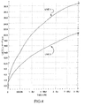
- Figure 4 represents a comparison between the rise time of the charge pump according to the present invention (represented by Line 1) and the rise time of the conventional pump (represented by Line 2). As shown in Figure 4, after the same amount of charging time, the output voltage of the charge pump according to the present invention is 33% greater than that of the conventional pump.
- Figure 5 represents a comparison of the charging characteristics of an eight stage charge pump according to the present invention (Line A) and the charging characteristics of a conventional pump also having eight stages (Line B) with both the conventional charge pump and the charge pump according to the present invention having the same last stage capacitor size.
- the output voltage generated by the charge pump according to the present invention (9.50) is 42% greater than that of the conventional pump (5.50) having the same number of stages.
- Figure 6 is a graph representing the rise time improvement of the charge pump according to the present invention over that of a conventional pump having the same area.
- a load capacitance, C L of 100 pF is coupled to the output of the circuit presented in Figure 2 and a load current, I load , of 20 ⁇ A is assumed.
- the conventional pump is represented as having 13 stages.
- the charge pump of the present invention is represented as having nine stages. The number of stages was determined by the inventors to have the fastest rise time for a given output voltage of 20V. Note, the curves presented in Figure 6 were generated by application of equations 3-10. As shown, the speed exhibited by the charge pump according to the present invention is much better than the speed of the conventional pump.
- Figure 6 also provides the means for determining the bootstrap coefficient, k, necessary to produce an optimized charge pump.
- the general rule is that the bootstrap coefficient, k, should be chosen according to the speed requirement.
- the speed requirement is about 1.5 ⁇ sec, a multiplication factor of 1.2 or greater is satisfactory. If the speed requirement is between 1.25 ⁇ sec and 1.5 ⁇ sec, a multiplication factor of 1.3 or greater is satisfactory. And for a speed requirement of about 1 ⁇ sec and less, a multiplication factor of 1.5 or greater is required.
- Figure 6 is also used to determine the overall area of the resulting charge pump.
- the steps used to determine the total area required for the charge pump are as follows:
- This procedure can be used to determine the total area for a charge pump having any number of stages and required rise times.
- the total area required for a charge pump having a rise time of about 2 ⁇ sec and delivering an output voltage of 20V is about 775 mil 2 .
- the conventional charge pump must be 2.3 times larger in size than the charge pump according to the present invention.
- the size of the capacitors for each stage of the charge pump can be determined.
- the steps used to determine the individual capacitor sizes is as follows:
Landscapes
- Engineering & Computer Science (AREA)
- Physics & Mathematics (AREA)
- General Physics & Mathematics (AREA)
- Microelectronics & Electronic Packaging (AREA)
- Nonlinear Science (AREA)
- Electromagnetism (AREA)
- Power Engineering (AREA)
- Radar, Positioning & Navigation (AREA)
- Automation & Control Theory (AREA)
- Dc-Dc Converters (AREA)
- Electromagnetic Pumps, Or The Like (AREA)
- Reciprocating Pumps (AREA)
- Catching Or Destruction (AREA)
Claims (8)
- Verfahren zum Bereitstellen einer Ladepumpenschaltung, mit folgenden Schritten:Bereitstellen einer Eingangseinrichtung (120) zum Empfangen eines Signals;Bereitstellen einer Ausgangseinrichtung zum Liefern eines modifizierten Signals; undBereitstellen mehrerer zwischen der Eingangs- und der Ausgangseinrichtung geschalteter Stufeneinrichtungen (150,122;152,124 ... 168, 138) zum Erzeugen des modifizierten Signals, wobei jede Stufeneinrichtung eine Kondensatoreinrichtung (122-138) aufweist, die derart ausgewählt ist, dass jede Stufeneinrichtung eine unterschiedliche Kapazität aufweist,wobei Cn die Kapazität der einen Kondensatoreinrichtung repräsentiert und Cn+1 die Kapazität der nächsten Kondensatoreinrichtung repräsentiert,
wobei die Kapazität Cn,Cn+1 sukzessiver von der Eingangseinrichtung zu der Ausgangseinrichtung verlaufender Stufeneinrichtungen auf einen Bootstrap-Koeffizienten k bezogen sind, der repräsentiert ist durch:
dadurch gekennzeichnet, dass
wobei m einen Multiplikationsfaktor repräsentiert und
ist und die Kapazität jeder jeweiligen Kondensatoreinrichtung anhand der Gesamtkapazität der Ladepumpe, einer Belastungskapazität der Ladepumpe und einer vorbestimmten Anstiegszeit ausgewählt ist. - Ladepumpenschaltung, die gemäß dem Verfahren nach Anspruch 1 bereitgestellt ist.
- Ladepumpenschaltung nach Anspruch 2, bei der die Ladepumpe eine Anzahl N von Stufeneinrichtungen aufweist, wobei N eine ganze Zahl größer als 2 ist.
- Ladepumpenschaltung nach Anspruch 3, bei der die Anzahl N von Stufeneinrichtungen gleich 9 ist.
- Ladepumpenschaltung nach einem der Ansprüche 2 bis 4, ferner mit einer zwischen jeder Stufeneinrichtung geschalteten Impedanzeinrichtung (121,123 ... 137).
- Ladepumpenschaltung nach Anspruch 5, bei der die Impedanzeinrichtung eine Diode aufweist.
- Ladepumpenschaltung nach Anspruch 5, bei der die Impedanzeinrichtung einen als Diode geschalteten MOS-Transistor aufweist.
- Ladepumpenschaltung nach einem der Ansprüche 2 bis 7, bei der k eine positive ganze Zahl größer als 0 ist.
Applications Claiming Priority (3)
| Application Number | Priority Date | Filing Date | Title |
|---|---|---|---|
| US08/672,095 US5818288A (en) | 1996-06-27 | 1996-06-27 | Charge pump circuit having non-uniform stage capacitance for providing increased rise time and reduced area |
| US672095 | 1996-06-27 | ||
| PCT/US1997/001332 WO1997050167A1 (en) | 1996-06-27 | 1997-01-28 | Charge pump circuit architecture |
Publications (2)
| Publication Number | Publication Date |
|---|---|
| EP0914707A1 EP0914707A1 (de) | 1999-05-12 |
| EP0914707B1 true EP0914707B1 (de) | 2006-05-31 |
Family
ID=24697129
Family Applications (1)
| Application Number | Title | Priority Date | Filing Date |
|---|---|---|---|
| EP97904030A Expired - Lifetime EP0914707B1 (de) | 1996-06-27 | 1997-01-28 | Schaltkreisarchitektur für ladungspumpen |
Country Status (5)
| Country | Link |
|---|---|
| US (2) | US5818288A (de) |
| EP (1) | EP0914707B1 (de) |
| DE (1) | DE69736001T2 (de) |
| TW (1) | TW339440B (de) |
| WO (1) | WO1997050167A1 (de) |
Families Citing this family (45)
| Publication number | Priority date | Publication date | Assignee | Title |
|---|---|---|---|---|
| US6373324B2 (en) | 1998-08-21 | 2002-04-16 | Intel Corporation | Voltage blocking method and apparatus for a charge pump with diode connected pull-up and pull-down on boot nodes |
| JP3477097B2 (ja) * | 1998-12-22 | 2003-12-10 | パイオニア株式会社 | 集積回路装置 |
| JP2000188374A (ja) * | 1998-12-22 | 2000-07-04 | Pioneer Electronic Corp | 昇圧電源回路及び半導体集積回路装置 |
| US6151229A (en) * | 1999-06-30 | 2000-11-21 | Intel Corporation | Charge pump with gated pumped output diode at intermediate stage |
| US6215702B1 (en) | 2000-02-16 | 2001-04-10 | Advanced Micro Devices, Inc. | Method of maintaining constant erasing speeds for non-volatile memory cells |
| DK200001482A (da) | 2000-10-05 | 2002-04-06 | Forskningsct Risoe | Elektrokemisk celle og fremgangsmåde til fremstilling af samme. |
| US6424570B1 (en) | 2001-06-26 | 2002-07-23 | Advanced Micro Devices, Inc. | Modulated charge pump with uses an analog to digital converter to compensate for supply voltage variations |
| US6535424B2 (en) | 2001-07-25 | 2003-03-18 | Advanced Micro Devices, Inc. | Voltage boost circuit using supply voltage detection to compensate for supply voltage variations in read mode voltage |
| US7023945B2 (en) * | 2002-06-17 | 2006-04-04 | Intel Corporation | Method and apparatus for jitter reduction in phase locked loops |
| US6798275B1 (en) | 2003-04-03 | 2004-09-28 | Advanced Micro Devices, Inc. | Fast, accurate and low power supply voltage booster using A/D converter |
| US7315438B2 (en) * | 2003-06-10 | 2008-01-01 | Seiko Epson Corporation | Technique to reduce ESD loading capacitance |
| US7023260B2 (en) * | 2003-06-30 | 2006-04-04 | Matrix Semiconductor, Inc. | Charge pump circuit incorporating corresponding parallel charge pump stages and method therefor |
| US7535281B2 (en) * | 2006-09-29 | 2009-05-19 | Micron Technology, Inc. | Reduced time constant charge pump and method for charging a capacitive load |
| US7477093B2 (en) * | 2006-12-31 | 2009-01-13 | Sandisk 3D Llc | Multiple polarity reversible charge pump circuit |
| US7495500B2 (en) * | 2006-12-31 | 2009-02-24 | Sandisk 3D Llc | Method for using a multiple polarity reversible charge pump circuit |
| US20090058507A1 (en) * | 2007-08-28 | 2009-03-05 | Prajit Nandi | Bottom Plate Regulated Charge Pump |
| US8044705B2 (en) | 2007-08-28 | 2011-10-25 | Sandisk Technologies Inc. | Bottom plate regulation of charge pumps |
| US7586362B2 (en) * | 2007-12-12 | 2009-09-08 | Sandisk Corporation | Low voltage charge pump with regulation |
| US7586363B2 (en) * | 2007-12-12 | 2009-09-08 | Sandisk Corporation | Diode connected regulation of charge pumps |
| US7969235B2 (en) | 2008-06-09 | 2011-06-28 | Sandisk Corporation | Self-adaptive multi-stage charge pump |
| US20090302930A1 (en) * | 2008-06-09 | 2009-12-10 | Feng Pan | Charge Pump with Vt Cancellation Through Parallel Structure |
| US8710907B2 (en) | 2008-06-24 | 2014-04-29 | Sandisk Technologies Inc. | Clock generator circuit for a charge pump |
| US7683700B2 (en) * | 2008-06-25 | 2010-03-23 | Sandisk Corporation | Techniques of ripple reduction for charge pumps |
| US7990741B2 (en) * | 2008-07-16 | 2011-08-02 | Aptina Imaging Corporation | Comparator controlled charge pump for negative voltage booster |
| US7795952B2 (en) * | 2008-12-17 | 2010-09-14 | Sandisk Corporation | Regulation of recovery rates in charge pumps |
| US7973592B2 (en) | 2009-07-21 | 2011-07-05 | Sandisk Corporation | Charge pump with current based regulation |
| US8339183B2 (en) | 2009-07-24 | 2012-12-25 | Sandisk Technologies Inc. | Charge pump with reduced energy consumption through charge sharing and clock boosting suitable for high voltage word line in flash memories |
| US8294509B2 (en) | 2010-12-20 | 2012-10-23 | Sandisk Technologies Inc. | Charge pump systems with reduction in inefficiencies due to charge sharing between capacitances |
| US8339185B2 (en) | 2010-12-20 | 2012-12-25 | Sandisk 3D Llc | Charge pump system that dynamically selects number of active stages |
| US8699247B2 (en) | 2011-09-09 | 2014-04-15 | Sandisk Technologies Inc. | Charge pump system dynamically reconfigurable for read and program |
| US8514628B2 (en) | 2011-09-22 | 2013-08-20 | Sandisk Technologies Inc. | Dynamic switching approach to reduce area and power consumption of high voltage charge pumps |
| US8400212B1 (en) | 2011-09-22 | 2013-03-19 | Sandisk Technologies Inc. | High voltage charge pump regulation system with fine step adjustment |
| US8710909B2 (en) | 2012-09-14 | 2014-04-29 | Sandisk Technologies Inc. | Circuits for prevention of reverse leakage in Vth-cancellation charge pumps |
| US8836412B2 (en) | 2013-02-11 | 2014-09-16 | Sandisk 3D Llc | Charge pump with a power-controlled clock buffer to reduce power consumption and output voltage ripple |
| US8981835B2 (en) | 2013-06-18 | 2015-03-17 | Sandisk Technologies Inc. | Efficient voltage doubler |
| US9024680B2 (en) | 2013-06-24 | 2015-05-05 | Sandisk Technologies Inc. | Efficiency for charge pumps with low supply voltages |
| US9077238B2 (en) | 2013-06-25 | 2015-07-07 | SanDisk Technologies, Inc. | Capacitive regulation of charge pumps without refresh operation interruption |
| US9007046B2 (en) | 2013-06-27 | 2015-04-14 | Sandisk Technologies Inc. | Efficient high voltage bias regulation circuit |
| US9083231B2 (en) | 2013-09-30 | 2015-07-14 | Sandisk Technologies Inc. | Amplitude modulation for pass gate to improve charge pump efficiency |
| US9154027B2 (en) | 2013-12-09 | 2015-10-06 | Sandisk Technologies Inc. | Dynamic load matching charge pump for reduced current consumption |
| US9491151B2 (en) * | 2015-01-07 | 2016-11-08 | Ememory Technology Inc. | Memory apparatus, charge pump circuit and voltage pumping method thereof |
| US9917507B2 (en) | 2015-05-28 | 2018-03-13 | Sandisk Technologies Llc | Dynamic clock period modulation scheme for variable charge pump load currents |
| US9647536B2 (en) | 2015-07-28 | 2017-05-09 | Sandisk Technologies Llc | High voltage generation using low voltage devices |
| US9520776B1 (en) | 2015-09-18 | 2016-12-13 | Sandisk Technologies Llc | Selective body bias for charge pump transfer switches |
| CN107453601B (zh) * | 2017-08-22 | 2023-09-19 | 合肥博雅半导体有限公司 | 电荷泵和存储器 |
Family Cites Families (8)
| Publication number | Priority date | Publication date | Assignee | Title |
|---|---|---|---|---|
| JPS5393350A (en) * | 1977-01-27 | 1978-08-16 | Canon Inc | Booster circuit |
| FR2437734A1 (fr) * | 1978-09-26 | 1980-04-25 | Thomson Csf | Amplificateur a capacites commutees, filtre a capacites commutees et filtre a transfert de charges comportant un tel amplificateur |
| US4554622A (en) * | 1983-09-22 | 1985-11-19 | Graco Inc | Compact voltage multiplier for spray guns |
| JPH03206457A (ja) * | 1989-10-18 | 1991-09-09 | Teijin Ltd | 消去可能な二層型有機光記録媒体 |
| JP3372556B2 (ja) * | 1991-07-23 | 2003-02-04 | 株式会社日立製作所 | 半導体集積回路 |
| US5301097A (en) * | 1992-06-10 | 1994-04-05 | Intel Corporation | Multi-staged charge-pump with staggered clock phases for providing high current capability |
| US5438504A (en) * | 1993-10-08 | 1995-08-01 | Sgs-Thomson Microelectronics, Inc. | Voltage multiplier circuits or the like |
| US5568035A (en) * | 1993-10-15 | 1996-10-22 | Sony/Tektronix Corporation | Variable-capacitance power supply apparatus |
-
1996
- 1996-06-27 US US08/672,095 patent/US5818288A/en not_active Expired - Lifetime
-
1997
- 1997-01-28 EP EP97904030A patent/EP0914707B1/de not_active Expired - Lifetime
- 1997-01-28 WO PCT/US1997/001332 patent/WO1997050167A1/en not_active Ceased
- 1997-01-28 DE DE69736001T patent/DE69736001T2/de not_active Expired - Lifetime
- 1997-02-05 TW TW086101408A patent/TW339440B/zh not_active IP Right Cessation
-
1998
- 1998-06-08 US US09/093,540 patent/US5973546A/en not_active Expired - Lifetime
Also Published As
| Publication number | Publication date |
|---|---|
| DE69736001D1 (de) | 2006-07-06 |
| WO1997050167A1 (en) | 1997-12-31 |
| TW339440B (en) | 1998-09-01 |
| US5973546A (en) | 1999-10-26 |
| US5818288A (en) | 1998-10-06 |
| DE69736001T2 (de) | 2007-01-11 |
| EP0914707A1 (de) | 1999-05-12 |
Similar Documents
| Publication | Publication Date | Title |
|---|---|---|
| EP0914707B1 (de) | Schaltkreisarchitektur für ladungspumpen | |
| Tanzawa et al. | A dynamic analysis of the Dickson charge pump circuit | |
| US6456152B1 (en) | Charge pump with improved reliability | |
| US5815446A (en) | Potential generation circuit | |
| US6747897B2 (en) | Semiconductor charge pump circuit and nonvolatile semiconductor memory device | |
| US6809573B2 (en) | Circuit for generating high voltage | |
| KR100230609B1 (ko) | 강유전성메모리디바이스감지증폭기용전치증폭기 | |
| US7071765B2 (en) | Boost clock generation circuit and semiconductor device | |
| US8120413B2 (en) | Charge pump circuit | |
| US6215329B1 (en) | Output stage for a memory device and for low voltage applications | |
| TW385540B (en) | Signal transmission method, signal transmission circuit, and semiconductor integrated circuit using the same | |
| KR100296861B1 (ko) | 전하 펌프 | |
| JPH01282796A (ja) | 不揮発性半導体記憶装置 | |
| EP0061271A1 (de) | Dynamische MOS-Speicheranordnung | |
| JP4730638B2 (ja) | 半導体装置 | |
| KR20030082239A (ko) | 저전압 승압 회로 | |
| JPH0923639A (ja) | 電圧変換装置 | |
| JPH0974738A (ja) | 半導体装置 | |
| JP2972723B2 (ja) | 半導体集積回路 | |
| JPH0284761A (ja) | 基準電圧発生回路 | |
| JPS6285669A (ja) | 昇圧回路 | |
| JPH08111092A (ja) | バッファ供給回路 | |
| JPH05234390A (ja) | 半導体集積回路装置 | |
| EP1159659A1 (de) | Vierphasenladungspumpe mit geringem spitzenstrom | |
| JPH023176A (ja) | 半導体メモリ回路 |
Legal Events
| Date | Code | Title | Description |
|---|---|---|---|
| PUAI | Public reference made under article 153(3) epc to a published international application that has entered the european phase |
Free format text: ORIGINAL CODE: 0009012 |
|
| 17P | Request for examination filed |
Effective date: 19990107 |
|
| AK | Designated contracting states |
Kind code of ref document: A1 Designated state(s): DE GB |
|
| 17Q | First examination report despatched |
Effective date: 20000810 |
|
| GRAP | Despatch of communication of intention to grant a patent |
Free format text: ORIGINAL CODE: EPIDOSNIGR1 |
|
| GRAS | Grant fee paid |
Free format text: ORIGINAL CODE: EPIDOSNIGR3 |
|
| GRAA | (expected) grant |
Free format text: ORIGINAL CODE: 0009210 |
|
| AK | Designated contracting states |
Kind code of ref document: B1 Designated state(s): DE GB |
|
| REG | Reference to a national code |
Ref country code: GB Ref legal event code: FG4D |
|
| REF | Corresponds to: |
Ref document number: 69736001 Country of ref document: DE Date of ref document: 20060706 Kind code of ref document: P |
|
| PLBE | No opposition filed within time limit |
Free format text: ORIGINAL CODE: 0009261 |
|
| STAA | Information on the status of an ep patent application or granted ep patent |
Free format text: STATUS: NO OPPOSITION FILED WITHIN TIME LIMIT |
|
| 26N | No opposition filed |
Effective date: 20070301 |
|
| PGFP | Annual fee paid to national office [announced via postgrant information from national office to epo] |
Ref country code: DE Payment date: 20160119 Year of fee payment: 20 |
|
| PGFP | Annual fee paid to national office [announced via postgrant information from national office to epo] |
Ref country code: GB Payment date: 20160127 Year of fee payment: 20 |
|
| REG | Reference to a national code |
Ref country code: DE Ref legal event code: R071 Ref document number: 69736001 Country of ref document: DE |
|
| REG | Reference to a national code |
Ref country code: GB Ref legal event code: PE20 Expiry date: 20170127 |
|
| PG25 | Lapsed in a contracting state [announced via postgrant information from national office to epo] |
Ref country code: GB Free format text: LAPSE BECAUSE OF EXPIRATION OF PROTECTION Effective date: 20170127 |