US7990741B2 - Comparator controlled charge pump for negative voltage booster - Google Patents
Comparator controlled charge pump for negative voltage booster Download PDFInfo
- Publication number
- US7990741B2 US7990741B2 US12/173,896 US17389608A US7990741B2 US 7990741 B2 US7990741 B2 US 7990741B2 US 17389608 A US17389608 A US 17389608A US 7990741 B2 US7990741 B2 US 7990741B2
- Authority
- US
- United States
- Prior art keywords
- voltage
- booster circuit
- terminal
- output
- charge pump
- Prior art date
- Legal status (The legal status is an assumption and is not a legal conclusion. Google has not performed a legal analysis and makes no representation as to the accuracy of the status listed.)
- Active, expires
Links
Images


Classifications
-
- H—ELECTRICITY
- H02—GENERATION; CONVERSION OR DISTRIBUTION OF ELECTRIC POWER
- H02M—APPARATUS FOR CONVERSION BETWEEN AC AND AC, BETWEEN AC AND DC, OR BETWEEN DC AND DC, AND FOR USE WITH MAINS OR SIMILAR POWER SUPPLY SYSTEMS; CONVERSION OF DC OR AC INPUT POWER INTO SURGE OUTPUT POWER; CONTROL OR REGULATION THEREOF
- H02M3/00—Conversion of dc power input into dc power output
- H02M3/02—Conversion of dc power input into dc power output without intermediate conversion into ac
- H02M3/04—Conversion of dc power input into dc power output without intermediate conversion into ac by static converters
- H02M3/06—Conversion of dc power input into dc power output without intermediate conversion into ac by static converters using resistors or capacitors, e.g. potential divider
- H02M3/07—Conversion of dc power input into dc power output without intermediate conversion into ac by static converters using resistors or capacitors, e.g. potential divider using capacitors charged and discharged alternately by semiconductor devices with control electrode, e.g. charge pumps
Definitions
- the present invention relates to the field of charge pumps and, more particularly, to methods and circuits for regulating charge pumps.
- charge pumps may be used for both of these purposes. Although a wide variety of charge pumps have been developed, many charge pumps use capacitors to obtain a boosted voltage or a voltage having a different polarity.
- a supply voltage is sampled on a first terminal of a capacitor (by charging the capacitor to the supply voltage) during a first phase of a cycle.
- one of the terminals is coupled to a load. If the first terminal of the capacitor is coupled to the load and the second terminal is held at ground, a boosted voltage may be generated. Because the capacitor was charged to the supply voltage during the first phase when the second terminal was connected to ground, the voltage on the first terminal is approximately twice the supply voltage during the second phase. If, during the second phase, the second terminal of the capacitor is coupled to the load and the first terminal is held at ground, a voltage with a reverse polarity may be generated.
- the voltage on the second terminal is approximately a negative supply voltage during the second phase.
- the charge pump repeatedly alternates between the first and second phases, each cycle generating an output voltage that is approximately twice the supply voltage V AA or of a reversed polarity.
- Charge pumps are presently used in a wide variety of applications. For example, charge pumps are typically used in memory devices to provide a negative substrate voltage or to provide a boosted voltage that may be applied to the gate of an NMOS transistor to allow the transistor to couple the supply voltage to an output node. Charge pumps are also used in CMOS imagers to generate voltages of different polarities and magnitudes during various operations carried out by the imagers. For example, charge pumps are commonly used to supply power having a polarity that is different from that of the supply voltage to the imaging array of CMOS imagers.
- the time required for a charge pump to output a target voltage is sometimes referred to as a time constant of the charge pump.
- the time constant of a charge pump driving a resistance load is very short as long as the current demands of the load do not exceed the current that may be supplied by the charge pump.
- the time constant, however, of a charge pump driving a capacitive load may be very long because the voltage applied to a load incrementally increases through a charge sharing process each cycle.
- the time constant of the charge pump may affect the magnitude of capacitance relative to the load capacitance, as well as the difference between the supply voltage and the load voltage to which the capacitive load has been charged.
- the charge pump thus, may be slow to reach the target voltage because the charge pump may not produce more charge than the combination of the pump capacitance, supply voltage and the load voltage.
- charge pumps typically do not compensate for charge lost when the charge pump is inactive.
- FIG. 1 is a schematic diagram of a charge pump according to one example of the invention.
- FIG. 2 is a schematic diagram of a charge pump according to another example of the invention including two voltage boosters arranged in counter-phase;
- FIG. 3 is a timing diagram of control signals and generated output voltage for the circuit shown in FIG. 1 ;
- FIG. 4 is a schematic diagram of a charge pump according to a further example of the invention.
- FIG. 5 is a timing diagram of generated output voltage and clock signals for the circuit shown in FIG. 4 ;
- FIG. 6 is a timing diagram of a voltage step signal generated by the charge pump shown in FIG. 4 when pumping charge from a load.
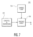
- FIG. 7 is a block diagram of a CMOS imager using one or more of the charge pumps shown in FIG. 1 , 2 or 4 or a charge pump according to another example of the invention.
- FIG. 1 illustrates a charge pump, designated generally as 100 , according one example of the invention.
- Charge pump 100 includes voltage booster circuit 102 , voltage regulator circuit 104 and clock generator 106 .
- Clock generator circuit 106 provides a set of nonoverlapping clock signals ( ⁇ 1 , ⁇ 2 ) to control voltage booster circuit 102 and voltage regulator circuit 104 .
- Clock signals ( ⁇ 1 , ⁇ 2 ) represent a first phase ( ⁇ 1 ) and second phase ( ⁇ 2 ) of a cycle.
- Voltage booster circuit 102 includes capacitance C p , two switches 110 , 112 that are closed during the first phase of each cycle and two switches 114 , 116 that are closed during the second phase of cycle. Voltage booster circuit 102 may be used to supply a negative voltage when powered by a positive supply voltage 118 of voltage V AA .
- a load L is connected to output node 126 of charge pump 100 . Switches 110 , 112 that are closed during the first phase of each cycle are open during the second phase, and switches 114 , 116 that are closed during the second phase are open during the first phase.
- the load L is assumed to be the array of a CMOS imager, which may be highly capacitance, with a capacitance of C L .
- Voltage booster circuit 102 is coupled to voltage regulator circuit 104 via node 128 and switch 114 . Voltage booster circuit 102 provides voltage V IN to voltage regulator circuit 104 via node 128 and receives regulator voltage V REG from voltage regulator circuit 104 via switch 114 .
- load L may not be entirely capacitive.
- load L may include both capacitor and diode components, where the diode may introduce some charge leakage.
- load L may correspond to transfer (TX) gates of active pixels (not shown) of a CMOS imager.
- voltage booster circuit 102 may be coupled to the TX gates via respective source diffusion regions of a number of driver transistors (not shown), for example, about 480-2500 driver transistors. Accordingly, there may be a significant load from respective forward-biased diffusion diodes of the corresponding pixels.
- the area of the diodes may be large enough to produce a detectable amount of charge leakage, even for driving voltages (i.e. V L ) for example, of about 250 mV below a threshold voltage of the diode.
- Voltage regulator circuit 104 includes supply voltage 120 of voltage V AA , capacitor C FB , switches 122 , 124 and differential amplifier 108 .
- Switch 122 is closed during the first phase of each cycle and switch 124 is closed during the second phase of each cycle.
- Switch 122 that is closed during first phase of each cycle is open during the second phase, and switch 124 that is closed during the second phase is open during the first phase.
- Switch 122 operates together with switch 110 , 112 and switch 124 operates in together with switches 114 , 116 .
- Capacitor C FB switches 122 , 124 and supply voltage 120 form level shift circuit 130 that receives voltage V IN from voltage booster circuit 102 generates level shifted voltage V SHIFT .
- Differential amplifier 108 receives a reference voltage V REF at the non-inverting input terminal and level shifted voltage V SHIFT at the inverting input terminal and produces regulation voltage V REG .
- Reference voltage V REF represents a target voltage corresponding to a desired negative pumping voltage. Accordingly, to reach an output level of ⁇ m volts (where m is an integer), reference voltage V REF can be set at (V AA ⁇ m).
- Capacitor C FB is a feedback capacitor which is used by differential amplifier 108 to detect load voltage V L . In general, capacitor C L is large, for example, 100 times larger, compared to capacitor C P .
- load L may include a diode component, which may introduce a charge leakage to load L. It may be appreciated that the charge leakage may increase exponentially with increasing voltage V L . Accordingly, a threshold voltage for the target voltage (and thus a suitable maxiumum reference voltage V REF ) may be determined such that charge pump 100 may compensate for the charge leakage. Charge pump 100 , thus, may produce a regulated load voltage V L that may substantially reduce noise due to charge leakage.
- supply voltage 122 is connected to an upper terminal of capacitor C P by switch 110 while switch 112 connects the lower terminal of capacitor C P to ground. Capacitor C P is therefore charged to ⁇ V AA during the first phase.
- supply voltage source 120 of voltage regulator circuit 104 is connected to one terminal of capacitor C FB , while switch 112 connects the other terminal of capacitor C FB to ground (i.e., such that V IN is at ground).
- differential amplifier 108 is disconnected from voltage booster circuit 102 and level shift circuit 102 , and capacitors C P and C FB are each charged to V AA .
- switch 114 is closed to connect the upper terminal of capacitor C P to receive regulation voltage V REG and the other switch 116 is closed to connect the other terminal of capacitor C P to load L.
- switch 124 is closed to connect one terminal of capacitor C FB to the inverting input terminal of differential amplifier 108 and the other terminal of C FB is connected to load L and thus to load voltage V L .
- a voltage difference of (V AA ⁇ V L ) is generated across level shift circuit 130 .
- differential amplifier 108 a feedback circuit is provided by differential amplifier 108 and capacitances C P , C FB . It may also be appreciated that voltage V SHIFT at the inverting input of differential amplifier 108 is at a voltage V AA higher than V L (i.e., it is level shifted). Differential amplifier 108 provides unity gain feedback from V REG to V L . Because of the feedback configuration, differential amplifier 108 adjusts V REG to compensate for any lost charge and to maintain output node 126 at a voltage of V REF ⁇ V AA .
- differential amplifier 108 In operation, when voltage regulator circuit 104 determines that load voltage V L is outside of a target voltage range, differential amplifier 108 slews to ground (for example, acting as a current sink), such that all charge across C P is pushed into load C L . Accordingly, both output node 126 and level shifted voltage V SHIFT are reduced by ⁇ (C P /C L ) ⁇ V AA . Thus, the entire supply voltage V AA range is used.
- differential amplifier 108 acting as a voltage buffer, generates regulation voltage V REG to provide sufficient charge into capacitor C P such that the inverting and non-inverting input terminals of differential amplifier 108 are maintained at a substantially same voltage.
- voltage regulator circuit 104 may 1) rapidly pump load L to within a target voltage range (where differential amplifer 108 acts as a current sink) and 2) apply differential amplifier 108 , acting as a voltage buffer, to reach the target voltage.
- a size of capacitor C P used in charge pump 100 , may be reduced. Because the size of capacitor C P may be reduced, a size of an output stage of differential amplifier 108 may also be reduced, thus generating a smaller output current. Accordingly, it may be appreciated that, even with the smaller output current differential amplifier 108 may still be capable of slewing from V AA to ground within a clock phase.
- voltage booster 102 may keep pumping within the full range (i.e., V AA ) until the load voltage V L is within the target voltage range. Because capacitor C P may be charged to supply voltage V AA , a size of capacitor C P may be reduced. Because the output voltage V IN of voltage booster circuit 102 is level shifted by a higher predetermined value (e.g., V AA ), voltage booster circuit 102 may be operated using a regulation voltage V REG , which generally produces for a larger voltage (compared to a target voltage) that may be used across capacitor C P . Because a larger voltage may be used in voltage booster circuit 102 , a capacitor size needed to reach a target voltage within the time constant may be reduced.
- the devices for implementing switches 110 , 112 , 114 , 116 , 122 , 124 are conventional as are circuitry for controlling them during the first and second phases of each cycle. Therefore, a more detailed explanation of these devices and control circuits have been omitted.
- FIG. 2 illustrates a charge pump, designated generally as 200 , according to another example of the invention.
- Charge pump 200 is the same as charge pump 100 ( FIG. 1 ) with an exception.
- charge pump 200 also includes a second voltage booster circuit 102 - 2 .
- Voltage booster circuits 102 - 1 , 102 - 2 are each connected to voltage regulator circuit 104 .
- Voltage booster circuit 102 - 2 includes switches 110 - 2 , 112 - 2 , 114 - 2 , 116 - 2 , capacitance C P and voltage source 118 - 2 .
- Switches 110 - 2 , 112 - 2 , 114 - 2 , 116 - 2 are operated out of phase with correspondingly numbered switches 110 - 1 , 112 - 1 , 114 - 1 , 116 - 1 .
- capacitor C P of voltage booster circuit 102 - 1 applies a voltage to load L during the second phase of each cycle and capacitor C P of voltage booster circuit 102 - 2 applies a voltage to load L during the first phase of each cycle.
- charge pumps 100 , 200 may include a gate (not shown) as part of clock generator 106 or separate from clock generator 106 .
- the gate may be used to inactivate voltage booster circuit 102 and/or voltage regulator circuit 104 at particular times. In this manner charge pump 100 , 200 ( FIGS. 1 and 2 ) may stop pumping, for example, during sampling of a pixel output of imager array to minimize the introduction of switch noise into sampled pixels.
- FIG. 3 a timing diagram of generated output voltage and control signals as a function of time are shown.
- FIG. 3 shows input clock signal 302 , pump clock signal 304 (i.e. ⁇ 1 , ⁇ 2 ), stop clock signal 306 , capacitive voltage signal 308 , load voltage signal 310 (i.e. V L ) and output voltage signal 312 .
- Input clock signal 302 is provided to clock generator 106 ( FIG. 1 ).
- Pump clock signal 304 is used to control charge pump 100 ( FIG. 1 ).
- Stop clock signal 306 is used to inactivate charge pump 100 ( FIG. 1 ), as described above.
- Capacitive voltage signal 308 represents a voltage capacitively coupled to load L that cycles during sampling.
- Load voltage signal 310 is the load voltage V L provided by charge pump 100 ( FIG. 1 ).
- Output voltage signal 312 represents a voltage of a single metal line across a CMOS imager array.
- load voltage signal 310 is pulled down rapidly after initialization.
- Load voltage signal 310 is shown to recover quickly after a hold period when a substantial amount of charge is pulled from the imager array. It may be seen that some of the coupling of the load to load voltage 310 during sampling (when stop clock signal 306 is asserted) may be accounted for by capacitive voltage signal 308 .
- capacitive voltage signal 308 When capacitive voltage signal 308 is pulled down, it also pulls down load voltage signal 310 , such that an amount of charge is leaked from output voltage signal 310 .
- load voltage signal 310 is initially less negative than prior to stop clock signal 306 being asserted.
- load voltage signal 310 is then reduced, thus, compensated by charge pump 100 ( FIG. 1 ). It may also be appreciated that charge lost to output voltage signal 312 , during the assertion of stop clock signal 306 , is also quickly compensated by charge pump 100 ( FIG. 1 ).
- FIG. 4 is a schematic diagram of a charge pump, designated generally as 400 , according to another example of the invention.
- Charge pump 400 includes voltage booster circuit 402 and regulator circuit 404 .
- Voltage booster circuit 402 supplies a negative voltage to output node 434 .
- Regulator circuit 404 generates a set of pump clock signals ( ⁇ 1 ′, ⁇ 2 ′) to control voltage booster circuit 402 .
- a capacitive load C L is connected to output node 434 of charge pump 400 and the voltage across capacitance load C L is designated as V L .
- pump clock signals ( ⁇ 1 ′, ⁇ 2 ′) are generated to activate and control operation of voltage booster circuit 402 when the load voltage V L at node 434 is less than a reference voltage V REF .
- load voltage V L is greater than or equal to reference voltage V REF
- pump clock signals ( ⁇ 1 ′, ⁇ 2 ′) are set to a low value (i.e. 0) and voltage booster circuit 402 is inactive.
- Pump clock signals ( ⁇ 1 ′, ⁇ 2 ′) represent a first phase ( ⁇ 1 ′) and second phase ( ⁇ 2 ′) of an active pump cycle.
- Voltage booster circuit 402 includes supply voltage 432 of voltage V AA , capacitor C P , two switches 424 , 426 that are closed during the first phase ( ⁇ 1 ′) of the pump cycle and two switches 428 , 430 that are closed during the second phase (® 2 ′) of the pump cycle. Switches 424 , 426 that are closed during the first phase of each cycle are open during the second phase. Switches 428 , 430 that are closed during the second phase are open during the first phase.
- Regulator circuit 404 includes voltage detector circuit 406 and clock generator circuit 408 .
- Voltage detector circuit 406 receives and samples load voltage V L from node 434 and provides a detected voltage V SENSE to clock generator circuit 408 .
- Clock generator circuit 408 generates a set of clock signals ( ⁇ 1 , ⁇ 2 ) to control voltage detector circuit 408 and the set of pump clock signals ( ⁇ 1 ′, ⁇ 2 ′) to control voltage booster circuit 402 .
- Clock signals ( ⁇ 1 , ⁇ 2 ) represent a first phase ( ⁇ 1 ) and second phase ( ⁇ 2 ) of a clock cycle. As described further below, clock signals ( ⁇ 1 , ⁇ 2 ) are generated each clock cycle.
- Voltage detector circuit 406 includes capacitor C s , first set of switches 416 , 418 and second set of switches 420 , 422 . Voltage detector circuit 406 receives and samples load voltage V L on capacitor C s according to the set of clock signals ( ⁇ 1 , ⁇ 2 ). Switches 416 , 418 that are closed during the first phase of each cycle are open during the second phase. Switches 420 , 422 that are closed during the second phase of each cycle are open during the first phase. During the second phase, capacitor C s samples load voltage V L when switches 420 , 422 are closed. During the first phase, switches 416 , 418 are closed and the detected voltage sampled by capacitor C s is inverted and provided to clock generator circuit 408 as detected voltage V SENSE .
- Clock generator circuit 408 includes comparator 410 , clock generator 412 and AND gates 414 - 1 , 414 - 2 .
- Comparator 410 compares detected voltage V SENSE with reference voltage V REF and generates a pump signal (pump). Comparator 410 generates a high pump signal (i.e., 1 ) when V SENSE is less than V REF . Comparator 410 generates a low pump signal (i.e., 0 ) when V SENSE is greater than or equal to V REF .
- Clock generator 412 generates the set of clock signals ⁇ 1 , ⁇ 2 which is provided to voltage detector circuit 406 , regardless of the state of the pump signal.
- Clock signals ⁇ 1 , ⁇ 2 are gated with the pump signal by AND 414 - 1 , 414 - 2 , respectively, to produce the set of pump clock signals ⁇ 1 ′, ⁇ 2 ′ used to control operation of voltage booster circuit 402 .
- Clock generator circuit 408 sets the set of pump clock signals ⁇ 1 ′, ⁇ 2 ′ to zero when the pump signal is low, thus causing pumping of voltage booster circuit 402 to cease.
- Reference voltage V REF represents a target voltage for the load voltage V L at output node 434 .
- V REF is a positive value of 400 mV, it is understood that any suitable reference voltage may be used, based on the load voltage.
- load L may also include a diode component that may generate a charge leakage. Accordingly, a suitable V REF may also be based on the charge leakage from the diode component.
- the set of clock signals ⁇ 1 , ⁇ 2 for clock generation circuit 406 continues for each cycle such that voltage detector circuit 406 continually detects load voltage V L .
- Voltage booster circuit 402 is activated when the pump signal is high.
- charge pump 400 may include first and second voltage booster circuits 402 (not shown), each connected to regulator circuit 404 .
- the first and second voltage booster circuits 402 are similar to each other except that they are operated out of phase. Accordingly, first and second voltage booster circuits 402 may apply a voltage to load L, as described above, during the first and second phases of each cycle, respectively.
- clock generator circuit 408 may be configured with a gate (not shown) to inactivate voltage booster circuit 402 at particular times. In this manner, charge pump 400 may stop pumping, for example, during sampling of a pixel output of imager array to minimize the introduction of switch noise into sampled pixels.
- FIG. 5 a timing diagram of a charge pump output voltage and clock sequences are shown for charge pump 400 .
- FIG. 5 shows input clock signal 502 , sense clock signal 504 (i.e., ⁇ 1 , ⁇ 2 ), pump clock signal 506 (i.e. ⁇ 1 ′, ⁇ 2 ), stop clock signal 508 , pump signal 510 , load voltage signal 512 (i.e. V L ) and output voltage signal 514 .
- Input clock signal 502 is provided to clock generator 412 ( FIG. 4 ).
- Sense clock signal 504 is used to control voltage detector circuit 406 ( FIG. 4 ).
- Pump clock signal 506 is used to control voltage booster circuit 402 ( FIG. 5 ).
- Stop clock signal 508 is used to inactivate charge pump 400 ( FIG. 4 ), as described above.
- Pump signal 510 is used in clock generator cirucit 408 ( FIG. 4 ) that is used to produce pump clock signal 506 .
- Load voltage signal 512 is the load voltage V L provided by charge pump 400 ( FIG. 4 ).
- Output voltage signal 514 represents a voltage of a single metal line across a CMOS imager array.
- voltage booster circuit 402 has a capacitance C P of 20 pF and a capacitive load C L of 5 nF. As shown in FIG. 5 , voltage booster circuit 402 is capable of pulling down capacitive load C L to ⁇ 0.5 V in less than 1.75 microseconds (load voltage signal 512 ). After load voltage signal 512 has reached the reference voltage, pump signal 510 is inactivated. When switching a load of 2 pF, voltage booster 402 ( FIG. 4 ) may compensate for lost charge within about 2 cycles. In contrast, conventional charge pumps typically have a start up time of about 30 microsecond with a 140 pF capacitor C P .
- load L may include a diode component that may contribute charge leakage.
- pump signal 510 may be activated at some interval to compensate for the charge leakage.
- FIG. 5 also illustrates that pump signal 510 may be triggered after release of stop clock signal 508 , in order to compensate for any charge leakage during inactivation of charge pump 400 ( FIG. 4 ).
- cycling of output voltage signal 514 may cause some charge leakage by the metal lines across the CMOS array. Accordingly, pump signal 510 is activated in order to compensate for the charge leakage during cycling of output voltage signal 514 .
- FIG. 6 a timing diagram illustrating a voltage step when pumping charge from a load is shown, for charge pump 400 ( FIG. 4 ).
- FIG. 6 shows input clock signal 602 , sense clock signal 604 (i.e., ⁇ 1 , ⁇ 2 ), pump clock signal 606 (i.e. ⁇ 1 ′, ⁇ 2 ′), stop clock signal 608 , pump signal 610 , load voltage signal 612 (i.e. V L ) and output voltage signal 614 .
- Signals 602 - 614 are similar to signals 502 - 514 , except that a different capacitive load is used.
- voltage booster 402 has a capacitance C P of 20 pF and a capacitive load C L of 4 nF.
- load voltage signal 612 slowly drifts upwards due to charge leakage (due to a diode component of load L) before it is pumped down (by activating pump signal 610 ) at about 3.08 microseconds.
- a small difference is illustrated between the transient responses (for example, between about 3.08 microseconds and about 3.1 microseconds) of load voltage signal 612 and output voltage signal 614 .
- the difference in the transient responses may be due to a resistance, capacitance (RC) delay between charge pump 400 ( FIG. 4 ) and output voltage 614 .
- the RC delay may reduce an amount of overshoot in output voltage 614 as compared with load voltage signal 612 .
- charge pumps 100 , 200 , 400 or a charge pump according to another example of the invention may be adapted to provide a positive rather than negative load voltage V L . Further, by adding additional switches and a capacitor, charge pumps 100 , 200 , 400 or a charge pump according to the other example of the invention may generate both positive and negative voltages.
- Charge pumps 100 , 200 , 400 or a charge pump according to some other example of the invention can be used in a wide variety of applications. They are particularly suitable for use in a CMOS imager because the imaging arrays of such devices are highly capacitive (as well as typically including a diode component that may generate a charge leakage).
- CMOS imager 700 shown in FIG. 7 include CMOS imaging array 706 that responds to a received image to generate corresponding signals.
- Array 706 is coupled to control and addressing circuit 702 , which interrogates imaging array 706 to output signal S i corresponding to the image received by imaging array 706 .
- CMOS imager 700 also includes charge pump 704 connected to imaging array 706 to supply imaging array 706 with a negative voltage.
- Charge pump 704 may be one of charge pumps 100 , 200 , 400 shown in respective FIG. 1 , 2 or 4 or a charge pump according to some other example of the invention.
Abstract
Description
Claims (15)
Priority Applications (1)
| Application Number | Priority Date | Filing Date | Title |
|---|---|---|---|
| US12/173,896 US7990741B2 (en) | 2008-07-16 | 2008-07-16 | Comparator controlled charge pump for negative voltage booster |
Applications Claiming Priority (1)
| Application Number | Priority Date | Filing Date | Title |
|---|---|---|---|
| US12/173,896 US7990741B2 (en) | 2008-07-16 | 2008-07-16 | Comparator controlled charge pump for negative voltage booster |
Publications (2)
| Publication Number | Publication Date |
|---|---|
| US20100013445A1 US20100013445A1 (en) | 2010-01-21 |
| US7990741B2 true US7990741B2 (en) | 2011-08-02 |
Family
ID=41529744
Family Applications (1)
| Application Number | Title | Priority Date | Filing Date |
|---|---|---|---|
| US12/173,896 Active 2029-10-15 US7990741B2 (en) | 2008-07-16 | 2008-07-16 | Comparator controlled charge pump for negative voltage booster |
Country Status (1)
| Country | Link |
|---|---|
| US (1) | US7990741B2 (en) |
Cited By (6)
| Publication number | Priority date | Publication date | Assignee | Title |
|---|---|---|---|---|
| US20120218032A1 (en) * | 2011-02-24 | 2012-08-30 | Rf Micro Devices, Inc. | High efficiency negative regulated charge-pump |
| US8547075B1 (en) * | 2011-06-08 | 2013-10-01 | Lattice Semiconductor Corporation | Voltage regulators with a shared capacitor |
| US20140306673A1 (en) * | 2013-04-11 | 2014-10-16 | Lion Semiconductor Inc. | Apparatus, systems, and methods for providing a hybrid power regulator |
| US9111601B2 (en) | 2012-06-08 | 2015-08-18 | Qualcomm Incorporated | Negative voltage generators |
| US10601311B2 (en) | 2018-02-13 | 2020-03-24 | Lion Semiconductor Inc. | Circuits and methods for hybrid 3:1 voltage regulators |
| US11043893B1 (en) | 2020-05-27 | 2021-06-22 | Nxp Usa, Inc. | Bias regulation system |
Families Citing this family (7)
| Publication number | Priority date | Publication date | Assignee | Title |
|---|---|---|---|---|
| US7948301B2 (en) * | 2009-08-28 | 2011-05-24 | Freescale Semiconductor, Inc. | Charge pump with charge feedback and method of operation |
| US8040700B2 (en) * | 2009-11-16 | 2011-10-18 | Freescale Semiconductor, Inc. | Charge pump for use with a synchronous load |
| US7965130B1 (en) | 2009-12-08 | 2011-06-21 | Freescale Semiconductor, Inc. | Low power charge pump and method of operation |
| CN104867465B (en) * | 2015-05-11 | 2017-08-25 | 深圳市华星光电技术有限公司 | Negative pressure signal generative circuit |
| US9564794B2 (en) * | 2013-12-04 | 2017-02-07 | Broadcom Corporation | System, apparatus, and method for a ping-pong charge pump |
| KR20210122932A (en) * | 2020-04-01 | 2021-10-13 | 삼성디스플레이 주식회사 | Power management circuit, method of generating a pixel power supplly voltage, and display device |
| US11489441B2 (en) * | 2020-06-02 | 2022-11-01 | Texas Instruments Incorporated | Reference voltage generation circuits and related methods |
Citations (15)
| Publication number | Priority date | Publication date | Assignee | Title |
|---|---|---|---|---|
| US5818288A (en) | 1996-06-27 | 1998-10-06 | Advanced Micro Devices, Inc. | Charge pump circuit having non-uniform stage capacitance for providing increased rise time and reduced area |
| US6018264A (en) | 1998-02-11 | 2000-01-25 | Lg Semicon Co., Ltd. | Pumping circuit with amplitude limited to prevent an over pumping for semiconductor device |
| US6320796B1 (en) | 2000-11-10 | 2001-11-20 | Marvell International, Ltd. | Variable slope charge pump control |
| US6359814B1 (en) | 2000-12-29 | 2002-03-19 | Intel Corporation | Negative output voltage charge pump and method therefor |
| US20020060917A1 (en) | 2000-11-17 | 2002-05-23 | Takashi Tanimoto | Voltage boost system |
| JP2004129377A (en) | 2002-10-02 | 2004-04-22 | Denso Corp | Charge pump boosting circuit |
| US6853567B2 (en) | 2002-11-28 | 2005-02-08 | Hynix Semiconductor Inc. | Pumping voltage generator |
| US20050030771A1 (en) | 2003-06-24 | 2005-02-10 | Stmicroelectronics S.R.L. | Low-consumption regulator for a charge pump voltage generator and related system and method |
| US6859091B1 (en) * | 2003-09-18 | 2005-02-22 | Maxim Integrated Products, Inc. | Continuous linear regulated zero dropout charge pump with high efficiency load predictive clocking scheme |
| US6903599B2 (en) | 2003-05-15 | 2005-06-07 | Amic Technology Corporation | Regulated charge pump |
| US20060279352A1 (en) | 2005-05-27 | 2006-12-14 | Tae-Whan Kim | Charge pump, DC-DC converter, and method thereof |
| US7276960B2 (en) | 2005-07-18 | 2007-10-02 | Dialog Semiconductor Gmbh | Voltage regulated charge pump with regulated charge current into the flying capacitor |
| US7279959B1 (en) | 2006-05-26 | 2007-10-09 | Freescale Semiconductor, Inc. | Charge pump system with reduced ripple and method therefor |
| US7310252B2 (en) | 2004-03-30 | 2007-12-18 | Micron Technology, Inc. | Closed-loop high voltage booster |
| US20080079479A1 (en) | 2006-09-29 | 2008-04-03 | Micron Technology, Inc. | Reduced time constant charge pump and method for charging a capacitive load |
-
2008
- 2008-07-16 US US12/173,896 patent/US7990741B2/en active Active
Patent Citations (15)
| Publication number | Priority date | Publication date | Assignee | Title |
|---|---|---|---|---|
| US5818288A (en) | 1996-06-27 | 1998-10-06 | Advanced Micro Devices, Inc. | Charge pump circuit having non-uniform stage capacitance for providing increased rise time and reduced area |
| US6018264A (en) | 1998-02-11 | 2000-01-25 | Lg Semicon Co., Ltd. | Pumping circuit with amplitude limited to prevent an over pumping for semiconductor device |
| US6320796B1 (en) | 2000-11-10 | 2001-11-20 | Marvell International, Ltd. | Variable slope charge pump control |
| US20020060917A1 (en) | 2000-11-17 | 2002-05-23 | Takashi Tanimoto | Voltage boost system |
| US6359814B1 (en) | 2000-12-29 | 2002-03-19 | Intel Corporation | Negative output voltage charge pump and method therefor |
| JP2004129377A (en) | 2002-10-02 | 2004-04-22 | Denso Corp | Charge pump boosting circuit |
| US6853567B2 (en) | 2002-11-28 | 2005-02-08 | Hynix Semiconductor Inc. | Pumping voltage generator |
| US6903599B2 (en) | 2003-05-15 | 2005-06-07 | Amic Technology Corporation | Regulated charge pump |
| US20050030771A1 (en) | 2003-06-24 | 2005-02-10 | Stmicroelectronics S.R.L. | Low-consumption regulator for a charge pump voltage generator and related system and method |
| US6859091B1 (en) * | 2003-09-18 | 2005-02-22 | Maxim Integrated Products, Inc. | Continuous linear regulated zero dropout charge pump with high efficiency load predictive clocking scheme |
| US7310252B2 (en) | 2004-03-30 | 2007-12-18 | Micron Technology, Inc. | Closed-loop high voltage booster |
| US20060279352A1 (en) | 2005-05-27 | 2006-12-14 | Tae-Whan Kim | Charge pump, DC-DC converter, and method thereof |
| US7276960B2 (en) | 2005-07-18 | 2007-10-02 | Dialog Semiconductor Gmbh | Voltage regulated charge pump with regulated charge current into the flying capacitor |
| US7279959B1 (en) | 2006-05-26 | 2007-10-09 | Freescale Semiconductor, Inc. | Charge pump system with reduced ripple and method therefor |
| US20080079479A1 (en) | 2006-09-29 | 2008-04-03 | Micron Technology, Inc. | Reduced time constant charge pump and method for charging a capacitive load |
Cited By (9)
| Publication number | Priority date | Publication date | Assignee | Title |
|---|---|---|---|---|
| US20120218032A1 (en) * | 2011-02-24 | 2012-08-30 | Rf Micro Devices, Inc. | High efficiency negative regulated charge-pump |
| US8461910B2 (en) * | 2011-02-24 | 2013-06-11 | Rf Micro Devices, Inc. | High efficiency negative regulated charge-pump |
| US8547075B1 (en) * | 2011-06-08 | 2013-10-01 | Lattice Semiconductor Corporation | Voltage regulators with a shared capacitor |
| US9111601B2 (en) | 2012-06-08 | 2015-08-18 | Qualcomm Incorporated | Negative voltage generators |
| US20140306673A1 (en) * | 2013-04-11 | 2014-10-16 | Lion Semiconductor Inc. | Apparatus, systems, and methods for providing a hybrid power regulator |
| US9143032B2 (en) * | 2013-04-11 | 2015-09-22 | Lion Semiconductor Inc. | Apparatus, systems, and methods for providing a hybrid power regulator |
| US10063139B2 (en) | 2013-04-11 | 2018-08-28 | Lion Semiconductor Inc. | Apparatus, systems, and methods for providing a hybrid voltage regulator |
| US10601311B2 (en) | 2018-02-13 | 2020-03-24 | Lion Semiconductor Inc. | Circuits and methods for hybrid 3:1 voltage regulators |
| US11043893B1 (en) | 2020-05-27 | 2021-06-22 | Nxp Usa, Inc. | Bias regulation system |
Also Published As
| Publication number | Publication date |
|---|---|
| US20100013445A1 (en) | 2010-01-21 |
Similar Documents
| Publication | Publication Date | Title |
|---|---|---|
| US7990741B2 (en) | Comparator controlled charge pump for negative voltage booster | |
| US6617832B1 (en) | Low ripple scalable DC-to-DC converter circuit | |
| US7541859B2 (en) | Charge pump circuit | |
| US7405549B2 (en) | Soft start circuit, power supply unit and electric equipment | |
| US20150015323A1 (en) | Charge pump circuit | |
| US20140268936A1 (en) | Ultra low-voltage circuit and method for nanopower boost regulator | |
| US8896367B1 (en) | Charge pump system | |
| US8963624B2 (en) | Boosting circuit | |
| US11632049B2 (en) | DC-DC converter and display device having the same | |
| WO2006085632A1 (en) | Power supply circuit and portable apparatus | |
| US11303257B2 (en) | Current sensor integrated circuit with common mode voltage rejection | |
| US20070063762A1 (en) | Semiconductor device with charge pump booster circuit | |
| US7724073B2 (en) | Charge pump circuit | |
| US7479811B2 (en) | Sample/hold circuit module | |
| CN109845081B (en) | Bootstrap circuit for DC/DC converter | |
| US10686377B1 (en) | Start-up method and apparatus for boost converters | |
| TWI684088B (en) | Voltage generator | |
| US7368978B2 (en) | Self regulating charge pump | |
| US9762225B2 (en) | Power supply apparatus and control method thereof | |
| JP2016059222A (en) | Integrated circuit device, display panel driver, display divice, and boosting method | |
| KR20160103298A (en) | Voltage generator and image sensing device with the same | |
| US10566898B1 (en) | Negative voltage circuit | |
| CN114070057A (en) | Voltage converter and method | |
| CN115437449A (en) | Clock booster circuit, on-chip high voltage generation circuit and electronic device | |
| US10044260B2 (en) | Charge pump circuit and voltage generating device including the same |
Legal Events
| Date | Code | Title | Description |
|---|---|---|---|
| AS | Assignment |
Owner name: MICRON TECHNOLOGY, INC.,IDAHO Free format text: ASSIGNMENT OF ASSIGNORS INTEREST;ASSIGNOR:MARTINUSSEN, TORE;REEL/FRAME:021264/0139 Effective date: 20080704 Owner name: MICRON TECHNOLOGY, INC., IDAHO Free format text: ASSIGNMENT OF ASSIGNORS INTEREST;ASSIGNOR:MARTINUSSEN, TORE;REEL/FRAME:021264/0139 Effective date: 20080704 |
|
| AS | Assignment |
Owner name: APTINA IMAGING CORPORATION,CAYMAN ISLANDS Free format text: ASSIGNMENT OF ASSIGNORS INTEREST;ASSIGNOR:MICRON TECHNOLOGY, INC.;REEL/FRAME:023159/0424 Effective date: 20081003 Owner name: APTINA IMAGING CORPORATION, CAYMAN ISLANDS Free format text: ASSIGNMENT OF ASSIGNORS INTEREST;ASSIGNOR:MICRON TECHNOLOGY, INC.;REEL/FRAME:023159/0424 Effective date: 20081003 |
|
| FEPP | Fee payment procedure |
Free format text: PAYOR NUMBER ASSIGNED (ORIGINAL EVENT CODE: ASPN); ENTITY STATUS OF PATENT OWNER: LARGE ENTITY |
|
| STCF | Information on status: patent grant |
Free format text: PATENTED CASE |
|
| FPAY | Fee payment |
Year of fee payment: 4 |
|
| MAFP | Maintenance fee payment |
Free format text: PAYMENT OF MAINTENANCE FEE, 8TH YEAR, LARGE ENTITY (ORIGINAL EVENT CODE: M1552); ENTITY STATUS OF PATENT OWNER: LARGE ENTITY Year of fee payment: 8 |
|
| MAFP | Maintenance fee payment |
Free format text: PAYMENT OF MAINTENANCE FEE, 12TH YEAR, LARGE ENTITY (ORIGINAL EVENT CODE: M1553); ENTITY STATUS OF PATENT OWNER: LARGE ENTITY Year of fee payment: 12 |