EP0909049A2 - Verfahren zur Regelung der Taktfrequenz eines drahtlosen Endgerätes - Google Patents
Verfahren zur Regelung der Taktfrequenz eines drahtlosen Endgerätes Download PDFInfo
- Publication number
- EP0909049A2 EP0909049A2 EP98250355A EP98250355A EP0909049A2 EP 0909049 A2 EP0909049 A2 EP 0909049A2 EP 98250355 A EP98250355 A EP 98250355A EP 98250355 A EP98250355 A EP 98250355A EP 0909049 A2 EP0909049 A2 EP 0909049A2
- Authority
- EP
- European Patent Office
- Prior art keywords
- receiving
- operation clock
- controlling
- inferential
- frequency
- Prior art date
- Legal status (The legal status is an assumption and is not a legal conclusion. Google has not performed a legal analysis and makes no representation as to the accuracy of the status listed.)
- Granted
Links
Images


Classifications
-
- H—ELECTRICITY
- H04—ELECTRIC COMMUNICATION TECHNIQUE
- H04B—TRANSMISSION
- H04B15/00—Suppression or limitation of noise or interference
- H04B15/02—Reducing interference from electric apparatus by means located at or near the interfering apparatus
- H04B15/04—Reducing interference from electric apparatus by means located at or near the interfering apparatus the interference being caused by substantially sinusoidal oscillations, e.g. in a receiver or in a tape-recorder
Definitions
- the present invention relates to a wireless communication terminal. More particularly, it relates to a digital wireless portable information terminal in accordance with a Time Division Multiplexing Access (TDMA) communication method.
- TDMA Time Division Multiplexing Access
- This type of digital wireless portable information terminal is constituted so as to include a wireless transmitting/receiving section and a data processing section processing data which this wireless transmitting/receiving section transmits and receives.
- Data processing is performed with a high speed clock (whose frequency is large) so that a CPU in the relevant data processing section operates at high speed.
- the objective of the present invention is to solve the problems of the prior art. Moreover, the objective is to provide a wireless communication terminal that can efficiently prevent noises vis-à-vis a wireless receiving section without employing a shield mechanism which requires space for packaging.
- the present invention which is a wireless communication terminal, is characterized in that it comprises a wireless transmitting/receiving section transmitting and receiving data, detecting means detecting the receiving electric field strength at the foregoing wireless transmitting/receiving section and operation clock control means controlling the frequency of an operation clock for processing data transmitted and received by the foregoing wireless transmitting/receiving section on the basis of a receiving electric field strength detected by the foregoing detecting means.
- the foregoing operation clock means is constituted so as to control the frequency of an operation clock to be come smaller as a receiving electric field strength becomes smaller.
- the wireless transmitting/receiving means has memory means memorizing the value of the receiving electric field strength.
- the operation clock control means is characterized in that it is constituted so as to control the frequency of an operation clock according to the receiving electric field strength memorized by this memory means.
- the wireless transmitting/receiving means performs transmitting/receiving processing in accordance with a Time Division Multiplexing Access (TDMA) communication method.
- the operation clock control means is characterized in, that it is constituted so as to control the frequency of an operation clock by its being synchronized with the timing of a time division receiving operation.
- the wireless transmitting/receiving means is constituted so as to generate an interrupt signal at a starting time of a receiving slot that is a timing of the time division receiving operation and an interrupt end signal at an ending time of said receiving slot.
- the operation clock control means is characterized in that it performs controlling the frequency of the foregoing operation clock according to the foregoing receiving electric field strength in response to the foregoing interrupt signal and ends off controlling the frequency of the foregoing operation clock in response to the foregoing interrupt end signal.
- the present invention will reduce noises generated from the data processing section and secure receiving performance without deteriorating processing performance of the data processing section so much by this means that the operation clock frequency of the CPU in the data processing section is constituted so as to be synchronized with a timing that a receiving slot of the wireless receiving section exists and be variably controlled according to a wireless receiving electric field strength.
- Fig. 1 is a block diagram of the embodiment of the present invention.
- reference numeral 1 is a wireless section which transmits and receives data in accordance with the Time Division Multiplexing Access (TDMA) commnunication method.
- Reference numeral 2 is a data processing section that processes data transmitted and received at the wireless section 1.
- TDMA Time Division Multiplexing Access
- the wireless section 1 has a wireless transmitting/receiving section 11, an interrupt signal generation section 12 for receiving a TCH (Transmission Channel) frame signal (a) sent from the wireless transmitting/receiving section 11 as an input and generating a receiving slot start interrupt signal (b) which is synchronized with a start timing of a receiving time slot and a receiving slot end interrupt signal (c) which is synchronized with an ending timing of the receiving time slot, and a receiving level inferential value memory section 13 for detecting and storing a receiving electric field strength at the wireless transmitting/receiving section 11.
- TCH Transmission Channel
- the data processing section 2 has a CPU 21 in which the operation clock frequency is variably controlled and data is processed with a controlled operation clock, its peripheral circuit 22, a display section of LCD 23 for performing various types of displays, a ROM 24 for read-only, a RAM 25 for freely read/write, and a data bus 26 for connecting respective these sections.
- the CPU 21 operates synchronizing with an operation clock which determines its operation speed.
- the frequency of this clock can be controlled according to a receiving level at the receiving level inferential value memory section 13.
- the timing of frequency control of the operation clock is controlled in response to a receiving slot start interrupt signal (b), and a clock frequency return is controlled in response to a receiving slot end interrupt signal (c).
- Fig. 2 is a timing chart showing the relationship between a TCH (Transmission Channel) frame signal (a) which is a standard interface signal utilized when performing data communication in accordance with the PDC (Personal Digital Cellular) method, a mobile unit receiving slot (receiving timing), a receiving slot start interrupt signal (b), and a receiving slot end interrupt signal (c).
- TCH Transmission Channel
- PDC Personal Digital Cellular
- a slot #0 is a receiving slot of a relevant terminal.
- a TCH frame (a) indicating a period of this slot #0 is active during the period and is led out from the wireless transmitting/receiving section 11 to the interrupt generation section 12.
- Both a start interrupt signal (b) which is synchronized with a starting timing of this TCH frame signal (a), and an end interrupt signal (c) which is synchronized with an end timing of the TCH frame signal (a) are generated from the interrupt generation section 12.
- the CPU 21 starts controlling an operation clock frequency in response to this start interrupt signal (b) and determines the clock frequency according to a receiving level inferential value stored at the receiving level inferential memory section 13.
- Fig. 3 is a graphical presentation showing the correlation between a receiving input level and a receiving level inferential value stored at the receiving level inferential value memory section 13 and also showing the cases indicated by three (3) stages in which respective receiving level inferential values are large, medium and small.
- the receiving level inferential value memory section 13 selects and memorizes a receiving level inferential value corresponding to a receiving electric field strength (a receiving input level) detected at the wireless transmitting/receiving section 11 according to the graphical presentation of the correlation shown in Fig. 3. According to Fig. 3, clock frequencies are variably controlled in compliance with receiving level inferential values of those three (3) stages.
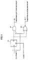
- Fig. 4 is a circuit diagram showing an example of the interrupt generation section 12.
- a TCH frame signal (a) is shown as data input supplied to a DFF (D-type Flip-Flop circuit) 121, and a clock signal is supplied to the DFF as a clock input.
- the reversed Q output of this DFF 122 is shown as an input supplied to an AND gate 122 and as an input supplied to an OR gate 123 respectively.
- a TCH frame signal (a) is supplied to the AND gate and to the OR gate respectively.
- a start interrupt signal (b) as an output outputted from the AND gate 122 and an end interrupt signal (c) as an output outputted from the OR gate 123 are led out respectively.
- Fig. 5A and Fig. 5B are flow charts showing processing operations of clock control of the CPU 21.
- Fig. 5A is a control flow chart in the case of receiving a receiving slot start interrupt signal, in which, responding to a start interrupt signal (Step 100), the CPU 21 reads out and determines a receiving level inferential value from the memory section 13 (Step 101). If the level is at the stage of "large” (Step 102), the clock frequency is not variably controlled (Step 103). Moreover, if the level is at the stage of "medium” (Step 104), the clock frequency is lowered to be 1/4 of the original frequency (Step 105). Furthermore, if the level is at the stage of "small” (Step 106), the clock frequency is lowered to be 1/16 of the original frequency (Step 107).
- Step 200 responding to a receiving slot end interrupt signal (c) (Step 200), the clock frequency is made to be returned to the original frequency (to the reference frequency before variable controlled) (Step 201).
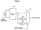
- Fig. 6 is a circuit block diagram for clock control, which includes a crystal oscillator 211 for oscillating a reference frequency signal, a PLL (Phase Locked Loop) circuit 212 for generating a clock phase-synchronized with an oscillation frequency of the crystal oscillator 211, dividers 213, 214 for making frequencies be 1/4 and 1/16 of the original frequencies by performing frequency division, and a selector 215 for selectively leading out one output out of an outputted from the PLL circuit 212 and frequency division outputs outputted from the dividers 213, 214.
- PLL Phase Locked Loop
- Clock frequency is freely controlled by the selector 215 selecting control according to a clock control signal on the basis of a receiving level inferential value read out from the receiving level inferential value memory section 13.
- the selector 215 selects an output outputted from the PLL circuit 212, selects an output outputted from the divider 213 if the receiving level inferential value is at the stage of "medium”, and selects an output outputted from the divider 214 if the receiving level inferential value is at the stage of "small".
- noise generation at the receiving section can be prevented by reducing the frequency of an operation clock of the CPU in the case where a receiving electric field is weak at a timing that a receiving slot exists, and in the other cases, an effect of noise reduction can be obtained by the clock frequent remaining to be at a high speed without sacrificing data processing speed.
Landscapes
- Engineering & Computer Science (AREA)
- Computer Networks & Wireless Communication (AREA)
- Signal Processing (AREA)
- Synchronisation In Digital Transmission Systems (AREA)
- Mobile Radio Communication Systems (AREA)
- Noise Elimination (AREA)
- Time-Division Multiplex Systems (AREA)
Applications Claiming Priority (3)
| Application Number | Priority Date | Filing Date | Title |
|---|---|---|---|
| JP274903/97 | 1997-10-08 | ||
| JP27490397 | 1997-10-08 | ||
| JP9274903A JPH11112442A (ja) | 1997-10-08 | 1997-10-08 | 無線通信端末 |
Publications (3)
| Publication Number | Publication Date |
|---|---|
| EP0909049A2 true EP0909049A2 (de) | 1999-04-14 |
| EP0909049A3 EP0909049A3 (de) | 2003-01-22 |
| EP0909049B1 EP0909049B1 (de) | 2010-03-10 |
Family
ID=17548143
Family Applications (1)
| Application Number | Title | Priority Date | Filing Date |
|---|---|---|---|
| EP98250355A Expired - Lifetime EP0909049B1 (de) | 1997-10-08 | 1998-10-07 | Verfahren zur Regelung der Taktfrequenz eines drahtlosen Endgerätes |
Country Status (4)
| Country | Link |
|---|---|
| US (1) | US6894982B1 (de) |
| EP (1) | EP0909049B1 (de) |
| JP (1) | JPH11112442A (de) |
| DE (1) | DE69841542D1 (de) |
Cited By (1)
| Publication number | Priority date | Publication date | Assignee | Title |
|---|---|---|---|---|
| US7093765B2 (en) * | 2000-02-04 | 2006-08-22 | Giesecke & Devrient Gmbh | Transponder, especially for a contactless chip card |
Families Citing this family (6)
| Publication number | Priority date | Publication date | Assignee | Title |
|---|---|---|---|---|
| US7920897B2 (en) * | 2002-03-14 | 2011-04-05 | Intel Corporation | Interference suppression in computer radio modems |
| JP2004193951A (ja) * | 2002-12-11 | 2004-07-08 | Nec Saitama Ltd | 携帯電話装置および携帯電話装置における受信感度劣化防止方法並びにプログラム |
| US7433393B2 (en) * | 2004-07-23 | 2008-10-07 | Nxp B.V. | Apparatus for controlling a digital signal processor for radio isolation and associated methods |
| US7895461B2 (en) | 2007-07-31 | 2011-02-22 | Hewlett-Packard Development Company, L.P. | Clock shifting and prioritization system and method |
| JP5644766B2 (ja) * | 2009-09-09 | 2014-12-24 | 日本電気株式会社 | 時分割通信装置およびその受信妨害防止方法 |
| US20120250745A1 (en) * | 2011-04-01 | 2012-10-04 | Novatel Wireless, Inc. | System and method for rf interference mitigation through memory clock frequency control |
Citations (1)
| Publication number | Priority date | Publication date | Assignee | Title |
|---|---|---|---|---|
| US5630224A (en) | 1994-12-29 | 1997-05-13 | Motorola, Inc. | Method and apparatus for avoiding desensitization of a radio frequency receiver |
Family Cites Families (11)
| Publication number | Priority date | Publication date | Assignee | Title |
|---|---|---|---|---|
| US4317181A (en) * | 1979-12-26 | 1982-02-23 | Texas Instruments Incorporated | Four mode microcomputer power save operation |
| US5222255A (en) * | 1991-08-05 | 1993-06-22 | Ford Motor Company | Intermodulation controller for radio receiver |
| DE69331165T2 (de) * | 1992-01-31 | 2002-05-16 | Canon K.K., Tokio/Tokyo | Tragbares elektronisches Gerät mit Funksendeempfänger und Rechnereinheit |
| JP3052576B2 (ja) * | 1992-06-09 | 2000-06-12 | 日本電気株式会社 | 表示付き無線選択呼出受信機 |
| WO1994006213A1 (en) * | 1992-09-02 | 1994-03-17 | Motorola, Inc. | Radio receiver |
| JPH06132837A (ja) * | 1992-10-20 | 1994-05-13 | Oki Electric Ind Co Ltd | 信号受信処理装置 |
| US5450086A (en) * | 1993-12-03 | 1995-09-12 | Texas Instruments Deutschland Gmbh | Self-tuning receiver/decoder for frequency shift keying RF data transmission |
| US5604745A (en) * | 1994-06-28 | 1997-02-18 | Nec Corporation | TDMA mobile telephone apparatus |
| JPH08166889A (ja) | 1994-12-13 | 1996-06-25 | Toshiba Corp | 情報処理装置及び情報処理方法 |
| US5848281A (en) * | 1996-07-23 | 1998-12-08 | Smalley; Kenneth George | Method and apparatus for powder management in a multifunction controller with an embedded microprocessor |
| JPH11205168A (ja) * | 1998-01-07 | 1999-07-30 | Nec Corp | 無線通信機能を有する情報処理装置及び動作クロック制御方法 |
-
1997
- 1997-10-08 JP JP9274903A patent/JPH11112442A/ja active Pending
-
1998
- 1998-10-06 US US09/167,267 patent/US6894982B1/en not_active Expired - Fee Related
- 1998-10-07 EP EP98250355A patent/EP0909049B1/de not_active Expired - Lifetime
- 1998-10-07 DE DE69841542T patent/DE69841542D1/de not_active Expired - Lifetime
Patent Citations (1)
| Publication number | Priority date | Publication date | Assignee | Title |
|---|---|---|---|---|
| US5630224A (en) | 1994-12-29 | 1997-05-13 | Motorola, Inc. | Method and apparatus for avoiding desensitization of a radio frequency receiver |
Cited By (1)
| Publication number | Priority date | Publication date | Assignee | Title |
|---|---|---|---|---|
| US7093765B2 (en) * | 2000-02-04 | 2006-08-22 | Giesecke & Devrient Gmbh | Transponder, especially for a contactless chip card |
Also Published As
| Publication number | Publication date |
|---|---|
| US6894982B1 (en) | 2005-05-17 |
| JPH11112442A (ja) | 1999-04-23 |
| DE69841542D1 (de) | 2010-04-22 |
| EP0909049A3 (de) | 2003-01-22 |
| EP0909049B1 (de) | 2010-03-10 |
Similar Documents
| Publication | Publication Date | Title |
|---|---|---|
| US6850754B2 (en) | Information processing apparatus and clock control method | |
| US6339422B1 (en) | Display control circuit and display control method | |
| US20090088194A1 (en) | Single Multi-Mode Clock Source for Wireless Devices | |
| EP0176818A2 (de) | Temperaturkompensierter Oszillator | |
| US6564040B1 (en) | Communication device and communication method | |
| US6894982B1 (en) | Wireless communication terminal and method of controlling operation clock for processing transmitting/receiving data in the same | |
| JP2002290340A (ja) | 情報処理装置、クロック制御方法 | |
| KR100309941B1 (ko) | 무선휴대단말기 | |
| US6072370A (en) | Clock extraction circuit | |
| JP4045842B2 (ja) | ドップラ偏移により生じたエラーを補正する方法及びその装置 | |
| CN119696614A (zh) | 天线状态控制方法、芯片、电子设备和可读存储介质 | |
| US7193621B2 (en) | Method for setting a pixel clock of a display driving circuit | |
| KR100547537B1 (ko) | 무선 통신기, 무선 전화기, 표시 동작 제어 방법, 및 컴퓨터 판독 가능한 프로그램이 기재된 기록 매체 | |
| JP4073431B2 (ja) | 地上子検出装置 | |
| JP2000112756A (ja) | Cpu動作制御装置および方法 | |
| CN106961275A (zh) | 一种实现电流控制的方法及装置 | |
| JP2017139656A (ja) | 無線通信端末 | |
| US20250125886A1 (en) | Oscillation frequency control method and system, and display device | |
| KR100206462B1 (ko) | 주파수도약방식의 통신시스템을 위한 위상동기루프 | |
| US6088776A (en) | Burst clock memory circuit | |
| JP3539443B2 (ja) | クロック発振回路を備えた受信機 | |
| JPH11168405A (ja) | 無線回路とそれを用いた移動無線機 | |
| JP2003347933A (ja) | クロック生成回路 | |
| KR100306764B1 (ko) | 디지털 비디오 카메라의 위상폐루프 클럭주파수자동조정방법 | |
| JPH06224792A (ja) | ラジオ受信機 |
Legal Events
| Date | Code | Title | Description |
|---|---|---|---|
| PUAI | Public reference made under article 153(3) epc to a published international application that has entered the european phase |
Free format text: ORIGINAL CODE: 0009012 |
|
| AK | Designated contracting states |
Kind code of ref document: A2 Designated state(s): AT BE CH CY DE DK ES FI FR GB GR IE IT LI LU MC NL PT SE |
|
| AX | Request for extension of the european patent |
Free format text: AL;LT;LV;MK;RO;SI |
|
| PUAL | Search report despatched |
Free format text: ORIGINAL CODE: 0009013 |
|
| AK | Designated contracting states |
Kind code of ref document: A3 Designated state(s): AT BE CH CY DE DK ES FI FR GB GR IE IT LI LU MC NL PT SE |
|
| AX | Request for extension of the european patent |
Free format text: AL;LT;LV;MK;RO;SI |
|
| 17P | Request for examination filed |
Effective date: 20030210 |
|
| AKX | Designation fees paid |
Designated state(s): DE GB SE |
|
| 17Q | First examination report despatched |
Effective date: 20071113 |
|
| GRAP | Despatch of communication of intention to grant a patent |
Free format text: ORIGINAL CODE: EPIDOSNIGR1 |
|
| GRAS | Grant fee paid |
Free format text: ORIGINAL CODE: EPIDOSNIGR3 |
|
| GRAA | (expected) grant |
Free format text: ORIGINAL CODE: 0009210 |
|
| AK | Designated contracting states |
Kind code of ref document: B1 Designated state(s): DE GB SE |
|
| REG | Reference to a national code |
Ref country code: GB Ref legal event code: FG4D |
|
| REF | Corresponds to: |
Ref document number: 69841542 Country of ref document: DE Date of ref document: 20100422 Kind code of ref document: P |
|
| REG | Reference to a national code |
Ref country code: SE Ref legal event code: TRGR |
|
| PLBE | No opposition filed within time limit |
Free format text: ORIGINAL CODE: 0009261 |
|
| STAA | Information on the status of an ep patent application or granted ep patent |
Free format text: STATUS: NO OPPOSITION FILED WITHIN TIME LIMIT |
|
| 26N | No opposition filed |
Effective date: 20101213 |
|
| PG25 | Lapsed in a contracting state [announced via postgrant information from national office to epo] |
Ref country code: SE Free format text: LAPSE BECAUSE OF NON-PAYMENT OF DUE FEES Effective date: 20101008 |
|
| PGFP | Annual fee paid to national office [announced via postgrant information from national office to epo] |
Ref country code: DE Payment date: 20121003 Year of fee payment: 15 |
|
| REG | Reference to a national code |
Ref country code: GB Ref legal event code: 732E Free format text: REGISTERED BETWEEN 20130110 AND 20130116 |
|
| PGFP | Annual fee paid to national office [announced via postgrant information from national office to epo] |
Ref country code: GB Payment date: 20121003 Year of fee payment: 15 |
|
| REG | Reference to a national code |
Ref country code: DE Ref legal event code: R082 Ref document number: 69841542 Country of ref document: DE Representative=s name: STORK BAMBERGER PATENTANWAELTE, DE Effective date: 20130912 Ref country code: DE Ref legal event code: R081 Ref document number: 69841542 Country of ref document: DE Owner name: WARREN & LEWIS INVESTMENT CORPORATION, FALLS C, US Free format text: FORMER OWNER: NEC CORP., TOKYO, JP Effective date: 20130912 Ref country code: DE Ref legal event code: R081 Ref document number: 69841542 Country of ref document: DE Owner name: WARREN & LEWIS INVESTMENT CORPORATION, US Free format text: FORMER OWNER: NEC CORP., TOKYO, JP Effective date: 20130912 |
|
| GBPC | Gb: european patent ceased through non-payment of renewal fee |
Effective date: 20131007 |
|
| REG | Reference to a national code |
Ref country code: DE Ref legal event code: R119 Ref document number: 69841542 Country of ref document: DE Effective date: 20140501 |
|
| PG25 | Lapsed in a contracting state [announced via postgrant information from national office to epo] |
Ref country code: GB Free format text: LAPSE BECAUSE OF NON-PAYMENT OF DUE FEES Effective date: 20131007 |
|
| PG25 | Lapsed in a contracting state [announced via postgrant information from national office to epo] |
Ref country code: DE Free format text: LAPSE BECAUSE OF NON-PAYMENT OF DUE FEES Effective date: 20140501 |