EP0903841B1 - Convertisseur alternatif/alternatif - Google Patents
Convertisseur alternatif/alternatif Download PDFInfo
- Publication number
- EP0903841B1 EP0903841B1 EP96916327A EP96916327A EP0903841B1 EP 0903841 B1 EP0903841 B1 EP 0903841B1 EP 96916327 A EP96916327 A EP 96916327A EP 96916327 A EP96916327 A EP 96916327A EP 0903841 B1 EP0903841 B1 EP 0903841B1
- Authority
- EP
- European Patent Office
- Prior art keywords
- switch
- output
- transformer
- converter
- switches
- Prior art date
- Legal status (The legal status is an assumption and is not a legal conclusion. Google has not performed a legal analysis and makes no representation as to the accuracy of the status listed.)
- Expired - Lifetime
Links
Images


Classifications
-
- H—ELECTRICITY
- H02—GENERATION; CONVERSION OR DISTRIBUTION OF ELECTRIC POWER
- H02M—APPARATUS FOR CONVERSION BETWEEN AC AND AC, BETWEEN AC AND DC, OR BETWEEN DC AND DC, AND FOR USE WITH MAINS OR SIMILAR POWER SUPPLY SYSTEMS; CONVERSION OF DC OR AC INPUT POWER INTO SURGE OUTPUT POWER; CONTROL OR REGULATION THEREOF
- H02M7/00—Conversion of ac power input into dc power output; Conversion of dc power input into ac power output
- H02M7/02—Conversion of ac power input into dc power output without possibility of reversal
- H02M7/04—Conversion of ac power input into dc power output without possibility of reversal by static converters
- H02M7/12—Conversion of ac power input into dc power output without possibility of reversal by static converters using discharge tubes with control electrode or semiconductor devices with control electrode
- H02M7/21—Conversion of ac power input into dc power output without possibility of reversal by static converters using discharge tubes with control electrode or semiconductor devices with control electrode using devices of a triode or transistor type requiring continuous application of a control signal
- H02M7/217—Conversion of ac power input into dc power output without possibility of reversal by static converters using discharge tubes with control electrode or semiconductor devices with control electrode using devices of a triode or transistor type requiring continuous application of a control signal using semiconductor devices only
- H02M7/2173—Conversion of ac power input into dc power output without possibility of reversal by static converters using discharge tubes with control electrode or semiconductor devices with control electrode using devices of a triode or transistor type requiring continuous application of a control signal using semiconductor devices only in a biphase or polyphase circuit arrangement
-
- H—ELECTRICITY
- H02—GENERATION; CONVERSION OR DISTRIBUTION OF ELECTRIC POWER
- H02M—APPARATUS FOR CONVERSION BETWEEN AC AND AC, BETWEEN AC AND DC, OR BETWEEN DC AND DC, AND FOR USE WITH MAINS OR SIMILAR POWER SUPPLY SYSTEMS; CONVERSION OF DC OR AC INPUT POWER INTO SURGE OUTPUT POWER; CONTROL OR REGULATION THEREOF
- H02M5/00—Conversion of ac power input into ac power output, e.g. for change of voltage, for change of frequency, for change of number of phases
- H02M5/02—Conversion of ac power input into ac power output, e.g. for change of voltage, for change of frequency, for change of number of phases without intermediate conversion into dc
- H02M5/04—Conversion of ac power input into ac power output, e.g. for change of voltage, for change of frequency, for change of number of phases without intermediate conversion into dc by static converters
- H02M5/22—Conversion of ac power input into ac power output, e.g. for change of voltage, for change of frequency, for change of number of phases without intermediate conversion into dc by static converters using discharge tubes with control electrode or semiconductor devices with control electrode
- H02M5/225—Conversion of ac power input into ac power output, e.g. for change of voltage, for change of frequency, for change of number of phases without intermediate conversion into dc by static converters using discharge tubes with control electrode or semiconductor devices with control electrode comprising two stages of AC-AC conversion, e.g. having a high frequency intermediate link
Definitions
- the present invention relates to an AC/AC converter having the function of converting voltage/current of electrical energy, that is widely used in various electronic devices, domestic appliances, personal power generators, various industrial installations, and power generators etc.
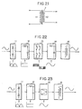
- a transformer such as that shown in Fig. 21, for example, is generally used as an AC transformer, which is a conventional AC/AC converter.
- this type of transformer has an output voltage regulated by a turns ratio of a primary winding to a secondary winding, which means that it is difficult to obtain an arbitrary voltage.
- the main materials for such a transformer are iron and copper, it becomes extremely heavy and large in size.
- reference numeral 11 is a rectifier
- reference numeral 12 is a smoothing circuit
- reference numeral 13 is an inverter
- reference numeral 14 is a high frequency filter
- reference numeral 15 is a step-up transformer.
- an AC input is rectified to DC by the rectifier 11
- ripple components are removed by the smoothing circuit 12
- output from the smoothing circuit 12 is subjected to high speed switching processing in the inverter 13 using well known PWM (pulse width modulation) control, turned back into low frequency AC by the high frequency filter 14, and converted as necessary to a desired voltage by the step-up transformer 15.
- PWM pulse width modulation
- an AC input is rectified by a rectifier 11
- an output of a smoothing circuit 12 is input to a power amplifier 16 and made into AC of a desired power, and converted to a desired voltage as required by the step-up transformer 15.
- Such AC control devices enable high speed control, for example, for an input fluctuation of ⁇ 20 % in a 100V AC input, an output of 100V ⁇ 0.1% is possible.
- step-up transformer 15 is a low frequency transformer, it becomes heavy and large in size, and there is a problem that it is difficult to reduce the size or weight of a device.
- U.S. Patent No. 3517300 discloses an AC/AC converter which is combined with a high frequency transformer by turning ON or OFF a semiconductor.
- the present invention improves these prior arts more practically by using connection shown for example in European Patent. No. 0618667 for bidirectional switches.
- the object of the present invention is to provide a high reliability AC/AC converter that is small in size and light in weight.
- each of the AC switches input AC is repeatedly conducted in alternately different directions in the primary winding of a transformer, at a frequency sufficiently higher than the frequency of the AC input. That is, the AC input is converted to high frequency. An arbitrary voltage dependent on the turns ratio of the transformer then appears at the secondary side of the transformer, still at the high frequency. Further, using the secondary side AC switches operating synchronously with the primary side AC switches, the conduction directions are made uniform again, close to the original waveform, to form a similar waveform. Since a high frequency is applied to the transformer in this way, it is possible to reduce the size of a transformer, and efficiency is also improved.
- the control means causes operation of the fifth AC switch and the sixth AC switch to be reversed when the AC input changes from a positive or negative half cycle to a negative or positive half cycle. In this way it is possible to simply change from an AC output to a DC output using the same structure.
- control means controls respective duty cycles (PWM) of the fifth AC switch and the sixth AC switch. In this way it is possible to simply obtain an arbitrary output voltage according to the duty cycle.
- PWM duty cycles
- the control means also controls respective pulse phases (PPM) of the fifth AC switch and the sixth AC switch. In this way, it is possible to easily obtain an arbitrary voltage according to the pulse phase.
- PPM pulse phases
- control means controls the duty cycle of one set of either the first AC switch and the second AC switch, or the third AC switch and the fourth AC switch.
- the output from the two ends of the secondary winding of the transformer is subjected to full wave rectification and used as one output end, while the center point of the secondary winding is used as the other output end.
- the fifth AC switch and the sixth AC switch are not required, so the circuit structure can be simplified and cost can also be reduced.
- the control means also controls respective duty cycles (PWM) for the fifth AC switch and the sixth AC switch in the above described circuit structure.
- PWM duty cycles
- the control means carries out pulse phase control (PPM), which is effectively the same as duty cycle control, continually varying the phase of a control signal for the fifth AC switch and the sixth AC switch from 0° to 90° with respect to the phase of a control signal for the first to fourth AC switches.
- PPM pulse phase control
- duty cycle control is carried out equivalent to continuously varying the phase of the control signal for the fifth AC switch and the sixth AC switch from 90° to 180° with respect to the phase of the control signal for the first to fourth AC switches.
- the position of the AC output is reversed, in the case of DC output the polarity of the DC output is inverted and it is thus possible to obtain an arbitrary voltage in response to duty cycle.
- one output terminal is connected to the full wave rectified output of the two terminals of the secondary winding of the transformer and another output terminal is connected to a center point of the secondary winding.
- the output of the above disclosed AC/AC converter and AC input can be combined to provide composite outputs.
- two voltages are combined and it is possible to obtain an arbitrary voltage from (input voltage + AC/AC converter output voltage) to (input voltage - AC/AC converter output voltage).
- Fig. 1A is a circuit diagram of an AC/AC converter of the first embodiment of the present invention.
- AC is an input AC supply
- reference numeral 1 is an input filter
- reference numeral 2 is an output filter
- reference numeral 3 is control means
- reference numeral S1 is a first AC switch
- S2 is a second AC switch
- S3 is a third AC switch
- S4 is a fourth AC switch
- S5 is a fifth AC switch
- S6 is a sixth AC switch
- S0 is an output switch taken as switch means.
- One end 4 and another end 5 of the input terminals are respectively connected to one end of an inductor L1 and one end of a capacitor C1, or one end of an inductor L1' and the other end of the capacitor C1, being input terminals of an the input filter 1, and also connected to control means 3 for operating a timing detector and the first to sixth AC switches S I - S6.
- the other end of the inductor L1 at one output of the input filter 1 is connected to one end of capacitor C2, and one end of the first AC switch S1 and the fourth AC switch S4, while the other end of the inductor L1' at the other end of the input filter 1 is connected to one end of the capacitor C3 and one end of the second AC switch S2 and the third AC switch S3.
- the other ends of the capacitor C2 and the capacitor C3 are connected to each other, as well as to contact a of a switch S0.
- the other end of the fourth AC switch S4 and the other end of the third AC switch S3 are connected together and also connected to one end of the primary winding n1 of the transformer T1, while the other end of the first AC switch S1 and the second AC switch S2 are connected together and also connected to contact b of the switch S0.
- a common terminal of the switch S0 is connected to the other end of the primary winding n1 of the transformer T1.
- the output switch S0 is connected to the side of the contact b.
- control terminals A - F of each of the AC switches S1 - S6 are respectively connected to control outputs A - F handled by control means 3.
- One end of the secondary winding n2 of the transformer T1 is connected to one end of the fifth AC switch S5, while the other end of the secondary winding n2 is connected to one end of the sixth AC switch S6.
- the other ends of the fifth AC switch S5 and the sixth AC switch S6 are respectively connected together and also connected to one end of an inductor L2 at one end of the output filter 2, while the center point of the secondary winding of the transformer T1 is connected to the other end of a capacitor C4 at the other end of the output filter 2 and also connected to another output terminal 7 through another output of the output filter 2.
- the other end of the inductor L2 of the output filter 2 is connected to one end of the capacitor C4, and also to output terminal 6 through one output of the output filter 2.
- each of the AC switches S1- S6 is shown in Fig. 2.
- Q1 and Q2 are semiconductor elements
- D1 and D2 are diodes.
- n channel MOSFETs are used in the semiconductor elements, which means that source electrodes of one polarity, being one of the terminals to be controlled of the semiconductor elements, are connected together, and alternating current AC is applied between the drains, being terminals to be controlled of another polarity.
- the diodes D1 and D2 are connected across the terminals to be controlled (D, S) of the n channel MOSFETs in the semiconductor elements Q1 and Q2, in the reverse direction to the conducting direction (which is drain to source).
- the cathodes of the diodes are respectively connected to the drain side of each FET, and the anodes are respectively connected to the source sides.
- the gates which are control terminals of the semiconductor elements Q1 and Q2
- the diodes D1 are not essential, and it is possible to obtain the same effects using the characteristics of semiconductor elements Q1 and Q2 depending on voltage resistance, current capacity, etc.
- Positive phase drive pulses for the AC switches S1, S3 and S5, and negative phase drive pulses for the AC switches S2, S4 and S6 are respectively supplied from the control means 3. If alternating current is input to the input terminals 4 and 5 of the AC/AC converter, an alternating voltage is respectively applied to one end of the AC switches S1 and S3, and one end of the AC switches S2 and S4, through the input filter 1. Each of the AC switches S1 - S4 is repeatedly switched between S1 and S3 being ON while S2 and S4 are OFF, and vice versa, as described above.
- AC current alternately flows via two paths having different directions for the transformer T, namely either path (1) AC switch S1 to transformer T to AC switch S3, or path (2) AC switch S4 to transformer T to AC switch S2.
- a half cycle of a commercial cycle is converted to high frequency bipolar. Namely, conversion is made to high frequency power that has been envelope modulated with the commercial cycle.
- An AC input that has been converted to high frequency in this way is applied to the primary winding n1 of the transformer T, and transferred to the secondary winding n2.
- the secondary winding n2 of the transformer T has its two ends respectively connected to the fifth AC switch S5 and the sixth AC switch S6, and the other ends of these two AC switches S5 and S6 are connected together and input to the output filter 2 as one output. Also, the center point of the secondary winding n2 of the transformer T is input to the output filter 2 as another output.
- AC switch S5 operates in synchronism with AC switches S1 and S3
- AC switch S6 operates in synchronism with AC switches S2 and S4. That is, they operate so that electric current always flows in only one direction in an AC half cycle.
- an AC input waveform that has been converted to high frequency by AC switches S1 and S3, or AC switches S2 and S4, is made into a waveform that approximates to or resembles the input AC voltage, by inverting the waveform in one direction and reconstituting it. That voltage is set to an arbitrary voltage according to the turns ratio of the transformer T, and high frequency components are removed by the output filter 2, and it is possible to obtain a desired voltage current waveform output that follows an input waveform from the output terminals 6 and 7.
- N1 - N4 are waveforms at nodes N1 - N4 in Fig. 1A.
- Fig. 3A shows control signals supplied from output terminals A - F of the AC/AC converter control means 3 to control terminals A - F corresponding to each of the AC switches S1 to S6, and in order to achieve the specific operation in this example, positive pulses applied to terminals A, C and E, and negative pulses applied to terminals B, D and F are respectively pulse waveforms having a duty cycle of approximately 50%.
- Fig. 3B shows a structural example of control means 3 for generating these type of control signals
- CLK is a clock signal generator
- FF is a flip-flop
- D is a D-type flip flop
- INV1 - INV3 are inverters
- PC1 - PC6 are photo couplers.
- a clock signal generated by the clock signal generator CLK is made into pulses of respective positive and negative phase by the flip-flop FF, and supplied to the photo couplers PC1, PC3 and PC5, or photo couplers PC2, PC4 and PC6.
- the clock signal from the clock signal generator CLK is supplied to the D-type flip flop, delayed by one pulse and drives each of the photo couplers as an inverted clock signal through the inverter INV3 together with the flip-flop signals.
- This is one example of such a circuit structure, but as long as the AC switches S1 - S6 are controlled at the above described timing, it is also possible to be constituted, for example, by an IC for PWM control, or a CPU and peripheral devices and a control program, etc.
- the operation will be described for the case when the output switch S0 is connected to the side of contact a.
- the contact a of the output switch S0 is connected between the capacitors C2 and the capacitor C3 connected in series. If these two capacitors C2 and C3 have the same capacitance, a potential at the connection point a of the output switch S0 becomes half the input voltage. Accordingly, when the output switch S0 is connected to the side of contact a, the virtual input becomes half, and the output voltage also becomes half. In this case, the AC switches S1 and S2 are not used. Therefore, in the case where voltage division is carried out using only the capacitors C2 and C3, these AC switches S1 and S2 can be omitted.
- Fig. 4 is a drawing showing waveforms at each section of a second embodiment of the present invention.
- the main circuit structure is the same as the circuit of Fig 1, and so description thereof will be omitted.
- waveforms at each of nodes N1 and N2 are the same as in the first embodiment, and the difference is that with respect to the waveform at nodes N3 and N4, the second half cycle of the AC waveform (II) is inverted to give direct current (pulsating current).
- Fig. 5A is a drawing showing output waveform timing of control signals of the control means carrying out the above described operation, and node N4.
- the operation of the fifth AC switch S5 and the sixth AC switch S6 in reversed by a discrimination signal HCS for discriminating the first half cycle (I) and the second half cycle (II) of the input signal.
- HCS discrimination signal
- Fig. 5B is a drawing showing a structural example of the control means 3 for supplying the above described control signals.
- the first half cycle and the second half cycle of the input signal are detected by a detector Det to output the discrimination signal HCS.
- Signals INV1 or INV2, which are positive logic or negative logic output signals from the flip flop FF, are selected by NOR gates 1 - 4 or NOR gates 5 - 8 using this discrimination signal HCS, to drive photo coupler PC5 or photo coupler PC6.
- the switch SW is a switch for selecting whether this type of DC output operation is carried out or the AC output operation of the first embodiment is carried out, and at the time of AC output is always at a high level, the discrimination signal HCS is not input to the NOR gate 4 and the NOR gate 8 to give normal operation.
- the rest of the structure is the same as that of the circuit in Fig. 3B, so the same structural elements have the same reference numerals attached, and description thereof is omitted.
- Fig. 6 is a drawing showing waveforms at each part in the third embodiment of the present invention.
- the main circuit structure is the same as the circuit of Fig. 1A and description thereof is omitted.
- waveforms at each of node N1 and node N2 are the same as in the first embodiment, but with respect to the waveform at node N3, the pulse width of each of the high frequency components when the AC waveform is restored is reduced and there is a period where current does not flow between each pulse, which means that the output waveform at node N4 is a lower (reduced) waveform than the input voltage (current) corresponding to the time that current does not flow in node N3. That is, duty cycle control of the AC switches S5 and S6 is carried out.
- Fig. 7A is a drawing showing the relationship between the control signals of the control means 3 for carrying out the above operation and the waveform of node N3.
- the waveform shown by a dotted line overlapping the waveform of node N3 is the output waveform of node N4.
- there is phase shift between the control signals of AC switches S1 and S3, and the control signal of AC switch S5, or between the control signals of AC switches S2 and S4 and the control signal of AC switch S6, and the period for which AC switch S5 and AC switch S6 are ON is reduced. Namely, for AC switches S1 and S3, or AC switches S2 and S4, the control signal of AC switch S5 or AC switch S6 is delayed by a fixed time, and the ON period is reduced.
- a pulse waveform appears at node N3 only in a period when AC switches S1 and S3 and AC switch S5 are active together, or when AC switches S2 and S4 and AC switch S6 are active together (in the drawing, portions of the control signals S5 and S6 shown with diagonal lines).
- the drive pulses of the AC switches S5 and S6 are delayed by 60° , the output becomes 2/3, while if the drive pulses are delayed by 180. the output becomes zero.
- Fig. 7B is a drawing showing a structural example of the control means 3 for supplying the above described control signals.
- Delay circuits DL1 and DL2 are respectively provided at the outputs of the NOR gates 1 and 5 of the circuit in Fig. 5B, but the remainder of the structure is the same as the circuit of Fig. 5, so description thereof will be omitted.
- This example has a structure with delay circuits DL1 and DL2 provided in the circuit of Fig. 5, but any structure is sufficient as long as the duty cycle of the control signals of AC switches S5 and S6 is controlled, and accordingly it is also possible to use a commercial PWM control IC etc.
- the AC switches S5 and S6 have been duty cycle controlled, but it is also possible, for example, to duty cycle control (PWM control) AC switches S1 and S3 and AC switches S2 and S4 in either direction, or in both directions, and the same effects can also be obtained in this case.
- PWM control duty cycle control
- Fig. 8 is a drawing showing waveforms at each section of a fourth embodiment of the present invention.
- the main circuit structure of the fourth embodiment is the same as the circuit of Fig. 1, and description thereof will be omitted.
- waveforms at each of the points N1 and N2 are the same as those in Fig 6, but with respect to the waveform at node N3, when the AC waveform is reconstituted the pulse amplitude of high frequency components has double peaks (positive side and negative side).
- the waveform at node N4 that has passed through the output filter 2 becomes a signal waveform having balanced pulse amplitude appearing at the positive and negative sides at node N3, namely a voltage value of a difference between positive and negative.
- phase control signals for the AC switches S5 and S6 with respect to the phase of control signals of the AC switches S1 - S4 (by delay or advance), the operation of the AC switches S1 and S3, and the operation of the AC switches S2 and S4 are changed while the AC switches S5 and S6 are ON, and an output voltage appears on the positive side and the negative side.
- PPM pulse phase modulation
- a pulse voltage appearing at node N3 will have equal amplitude in positive and negative directions, and equal pulse width and the average value is zero.
- Fig. 9A is a drawing showing the relationship between control signals of the control means 3 for carrying out the above described operation and the waveform at node N3.
- the waveform shown by a dotted line overlapping the waveform at node N3 is the output waveform at node N4.
- a waveform is shown for the case where the phase of control signals of the AC switches S5 and S6 has been delayed by 45° with respect to the control signals of AC switches S1 - S4.
- the AC switch S5 is ON there is a switch from AC switches S1 and S3 to AC switches S2 and S4, and at node N3 part of a pulse waveform appears from the positive side to the negative side.
- the waveform of Fig. 9A has a positive side pulse waveform narrower than the negative side and a waveform at node N4 that has passed through the output filter 2 has its phase inverted if it is an alternating waveform, or its polarity reversed if it is a direct current. That is, when the phase of control signals of the AC switches S5 and S6 is caused to vary continuously from 0° - 180° , it is possible to obtain an output that is continuous from a maximum positive phase value, through zero (90° ) to a maximum negative phase value. Also, in the case of direct current output, it is possible to continuously vary from a maximum positive DC voltage, through a zero voltage to a maximum negative DC voltage.
- Fig. 9B is a drawing showing a structural example of a control means 3 for supplying the above described control signals, and has cathode sides of the photo coupler PC5 and the photo coupler PC6 connected to ground through a resistor R.
- outputs from the photo coupler PC5 and the photo coupler PC6 can be changed in phase only without being affected by outputs from the D-type flip-flop D, and without changing the ON/OFF periods (waveform) using the detectors D11 and D12.
- the rest of the structure is the same as that in the circuit of Fig. 5B, and description thereof will be omitted.
- Fig. 10 shows a fifth embodiment of the present invention, in which the circuit of Fig. 1 is modified such that one end 4 of an input is connected to the other end (7), thereby constituting a circuit for extracting an output from a terminal 8 connected to one end 6 of the output and a terminal 9 connected to another end 5 of the input.
- the following voltage operation becomes possible.
- the phase of the control signals of the AC switches S5 and S6 from 0° - 360° in the case of PWM control or from 0° - 180° in the case of PPM control, an AC voltage appearing between the terminals 6 and 7 is varied from a maximum positive phase value through zero to a maximum negative phase value.
- V V1 ⁇ V1
- An integration regulator has the same function, but according to the present invention the capacitance and size can be made exceptionally small, and phase variation from input to output does not occur, making the device of the present invention excellent.
- Fig. 11 is a circuit diagram of a sixth embodiment of the present invention, and has diodes D51 and D52 acting as a full wave rectifying circuit replacing the AC switches S5 and S6 of the circuit in Fig. 1A.
- This is a device for DC only.
- diodes D53 and D54 are provided, inversely connected in series across another end of the inductor L2 of the output filter 2 and another of the output terminals 7, a series circuit comprising an inductor L3 and a capacitor C5 is connected across a center point of the two diodes D53 and D54 and another end of the inductor L2, and output ripple is reduced.
- the voltage rectification in this case can be duty cycle control of the control signals of the AC switches S1 and S3, and the AC switches S2 and S4.
- Fig. 12 - Fig. 15 showing a test circuit and measurement results of the test circuit for an AC/AC converter of the present invention.
- waveforms at each of the nodes N11 - N14 when the switching frequency is approximately 20 kHz are shown in Fig. 13A, Fig. 13B and Fig. 13C.
- the lower part of Fig. 13A is a waveform at node N11 while the upper half is a waveform at node N12 after being switched by AC switches S3 and AC switch S4.
- the lower part of Fig. 13B is the waveform at node N13, and although it is not clear from the drawing it actually includes high frequency components.
- FIG. 13B is a waveform at node N14, and high frequency components have been removed by the inductor L2 and the capacitor C4.
- the upper part of Fig. 13C is a waveform at node N12 with the frequency range expanded, for showing the situation when being modulated at high frequency.
- the lower part of Fig. 13C is the waveform at node N13 for showing the situation where the waveform of the upper part of Fig. 13C is modulated on the same polarity side (positive side) by the AC switches S5 and S6.
- Fig. 15A shows the waveforms at node N21 and node N22, with the waveform of node N22 being voltage divided by the capacitors C2 and C3 to become 1/2 of the waveform at node N21.
- the upper part and the lower part of Fig. 15B respectively show waveforms at nodes N23 and N24, and it will be understood that an input AC waveform is switched at high frequency to the positive side or the negative side by operation of the corresponding AC switch S4 or S3.
- FIG. 15C shows waveforms at nodes N25 and N26 of the primary winding or secondary winding of the transformer 1, and shows high frequency conversion by the AC switches S3 and S4 to give upper and lower waveforms.
- Fig. 15D shows an enlarged frequency range of a voltage waveform that has been modulated at high frequency (20 kHz) by the AC switches S3 and S4.
- Fig. 15E shows waveform of node N27 which is the waveform of node N26 after it has been rectified.
- Fig. 15F shows the voltage between the source and drain of MOSFETs which are semiconductor elements of the AC switches S3 and S4.
- Fig. 16A is a waveform diagram of waveforms measured at each section when PPM control has been carried out by the control means shown in Fig. 9B and the circuit of Fig. 1.
- a is a drawing of the input waveform at node N2 when the frequency range is enlarged
- b is a control signal for AC switch S5
- c is a control signal for AC switch S6
- d is a control signal for AC switches S1 - S4.
- the control signal for AC switch S5 (inverted AC switch S6) and the control signal for AC switches S1 - S4 have substantially the same phase, which means that the output voltage waveform becomes an AC waveform having maximum voltage in the positive phase, as shown in Fig. 16B.
- Fig. 17A is a waveform diagram of waveforms measured at each section when PPM control has been carried out by the control means shown in Fig. 9B and the circuit of Fig. 1.
- the reference numerals are the same as in Fig. 16A and description is omitted.
- the control signal for AC switch S5 inverted control signal for AC switch S6 is delayed by approximately 45° with respect to the control signal for the AC switches S1 - S4.
- the output voltage waveform becomes an AC voltage waveform with a level of 50% compared to the maximum voltage in the positive phase, as shown in Fig. 17B.
- Fig. 18A is a waveform diagram of waveforms measured at each section when PPM control has been carried out by the control means shown in Fig. 9B and the circuit of Fig. 1.
- the reference numerals are the same as in Fig. 16A and description is omitted.
- the control signal for AC switch S5 inverted AC switch S6
- the output voltage waveform becomes substantially zero, as shown in Fig. 18B.
- the waveform that appears longitudinally symmetrical in Fig. 18B is a noise component, and the average voltage is substantially zero volts.
- Fig. 19A is a waveform diagram of waveforms measured at each section when PPM control has been carried out by the control means shown in Fig. 9B and the circuit of Fig. 1.
- the reference numerals are the same as in Fig. 16A and description is omitted.
- the control signal for AC switch S5 inverted AC switch S6
- the output voltage waveform becomes an AC voltage waveform with a level of 50% compared to the maximum voltage in the negative phase, as shown in Fig. 19B.
- Fig. 20A is a waveform diagram of waveforms measured at each section when PPM control has been carried out by the control means shown in Fig. 9B and the circuit of Fig. 1.
- the reference numerals are the same as in Fig. 16A and description is omitted.
- the control signal for AC switch S6 inverted AC switch S5
- the control signal for AC switch S6 is substantially synchronous with the control signals for the AC switches S1 - S4. That is, it becomes phase inverted compared to the case of Fig. 16A.
- the output voltage waveform becomes an AC waveform having maximum voltage in the negative phase, as shown in Fig. 20B.
- an input AC supply is converted to high frequency by AC switches using semiconductor elements, and following that is rectified back to a waveform approximating to or resembling the input waveform, which means that:
Landscapes
- Engineering & Computer Science (AREA)
- Power Engineering (AREA)
- Ac-Ac Conversion (AREA)
- Inverter Devices (AREA)
Claims (8)
- Un convertisseur alternatif/alternatif ayant : connecté en série, un premier commutateur alternatif (S1) et un deuxième commutateur alternatif (S2) puis, connecté en série, un quatrième commutateur alternatif (S4) et un troisième commutateur alternatif (S3), respectivement reliés en parallèle à une borne (4) puis à une autre borne (5) d'une entrée alternative ; une borne d'une bobine primaire (n1) d'un transformateur (T) reliée entre lesdits premier commutateur alternatif (S1) et deuxième commutateur alternatif (S2), une autre borne de la bobine primaire (n1) dudit transformateur (T) étant reliée entre lesdits quatrième commutateur alternatif (S4) et troisième commutateur alternatif (S3) ; une borne d'une bobine secondaire (n2) dudit transformateur (T) étant relié à une borne d'un cinquième commutateur alternatif (S5), une autre borne de la bobine secondaire (n2) dudit transformateur (T) étant reliée à une borne d'un sixième commutateur alternatif (S6), les autres bornes des cinquièmes et sixièmes commutateurs alternatifs (S5, S6) étant respectivement reliées selon une sortie (6), avec une borne centrale de la bobine secondaire (n2) dudit transformateur (T) formant l'autre sortie (7) ; et fourni avec un dispositif de régulation (3) pour réaliser un fonctionnement alterné desdits premier commutateur alternatif (S1), troisième commutateur alternatif (S3) et cinquième commutateur alternatif (S5), ou desdits deuxième commutateur alternatif (S2), quatrième commutateur alternatif (S4) et sixième commutateur alternatif (S6), à une fréquence supérieure à celle d'une forme d'onde d'entrée ; caractérisée en ce qu'il comporte en outre deux condensateurs (C2, C3) reliés en série à une borne (4) et à une autre borne (5) de ladite entrée alternative, à une position plus proche de la borne d'entrée que de chaque commutateur alternatif de la face primaire du transformateur (T), et un dispositif de commutation (S0) pour basculer la connexion de ladite borne de la bobine primaire (n1 ) du transformateur (T) vers, soit la borne entre les deux condensateurs (C2, C3), soit la borne entre le premier commutateur alternatif (S1) ou le deuxième commutateur alternatif (S2).
- Le convertisseur alternatif/alternatif tel que décrit en revendication 1, dans lequel le dispositif de régulation (3) provoque l'inversion du fonctionnement du cinquième commutateur alternatif (S5) et du sixième commutateur alternatif (S6) lorsque l'entrée alternative passe d'un demi-cycle positif ou négatif à un demi-cycle négatif ou positif.
- Le convertisseur alternatif/alternatif tel que décrit en revendication 1, dans lequel le dispositif de régulation (3) commande les cycles d'utilisation (MLI - Modulation de Largeur d'impulsion) respectifs du cinquième commutateur alternatif (S5) et du sixième commutateur alternatif (S6).
- Le convertisseur alternatif/alternatif tel que décrit en revendication 1, dans lequel le dispositif de régulation (3) commande des phases d'impulsion (MIP - Modulation d'impulsion en Phase) respectives du cinquième commutateur alternatif (S5) et du sixième commutateur alternatif (S6).
- Le convertisseur alternatif/alternatif tel que décrit en revendication 1, dans lequel le dispositif de régulation (3) commande le cycle d'utilisation d'un ensemble, soit du premier commutateur alternatif (S1) et du deuxième commutateur alternatif (S2), soit du troisième commutateur alternatif (S3) et du quatrième commutateur alternatif (S4).
- Le convertisseur alternatif/alternatif tel que décrit en revendication 1, dans lequel la sortie des deux bornes de la bobine secondaire (n2) du transformateur (T) est soumise à un redressement pleine onde et est utilisé comme borne de sortie, tandis qu'une borne centrale de la bobine secondaire (n2) du transformateur (T) est utilisée comme autre borne de sortie.
- Un convertisseur alternatif/alternatif comportant une tension de sortie (V = V0 +/- V1) étant la somme de la sortie (+/-V1) et de la tension d'entrée alternative (V0) du convertisseur alternatif/alternatif tel que décrit dans la revendication 1.
- Un convertisseur alternatif/alternatif comportant une pluralité de convertisseurs alternatif/alternatif tel que décrit dans la revendication 1, et appliqué à un circuit triphasé.
Applications Claiming Priority (3)
| Application Number | Priority Date | Filing Date | Title |
|---|---|---|---|
| CN96180321A CN1074603C (zh) | 1996-06-06 | 1996-06-06 | Ac-ac/dc转换器 |
| CA002255918A CA2255918A1 (fr) | 1996-06-06 | 1996-06-06 | Convertisseur alternatif/alternatif |
| PCT/JP1996/001538 WO1997047070A1 (fr) | 1996-06-06 | 1996-06-06 | Convertisseur alternatif/alternatif |
Publications (3)
| Publication Number | Publication Date |
|---|---|
| EP0903841A1 EP0903841A1 (fr) | 1999-03-24 |
| EP0903841A4 EP0903841A4 (fr) | 1999-09-29 |
| EP0903841B1 true EP0903841B1 (fr) | 2004-08-11 |
Family
ID=27170885
Family Applications (1)
| Application Number | Title | Priority Date | Filing Date |
|---|---|---|---|
| EP96916327A Expired - Lifetime EP0903841B1 (fr) | 1996-06-06 | 1996-06-06 | Convertisseur alternatif/alternatif |
Country Status (6)
| Country | Link |
|---|---|
| US (1) | US6067243A (fr) |
| EP (1) | EP0903841B1 (fr) |
| CN (1) | CN1074603C (fr) |
| AU (1) | AU5034798A (fr) |
| CA (1) | CA2255918A1 (fr) |
| WO (1) | WO1997047070A1 (fr) |
Families Citing this family (42)
| Publication number | Priority date | Publication date | Assignee | Title |
|---|---|---|---|---|
| US6354516B1 (en) | 1999-11-02 | 2002-03-12 | Aradigm Corporation | Pore structures for reduced pressure aerosolization |
| JP3805927B2 (ja) * | 1999-06-10 | 2006-08-09 | 株式会社アイ・ヒッツ研究所 | 交流電圧調整器 |
| US6344985B1 (en) | 2000-12-05 | 2002-02-05 | Heart Transverter S.A. | Multiple port bi-directional power converter |
| DE10162214B4 (de) * | 2000-12-19 | 2014-02-13 | Denso Corporation | Kraftfahrzeug-Motor-/Generatorgerät mit Synchronmaschine |
| ES2183712B1 (es) * | 2001-05-11 | 2003-10-16 | Domenech Manuel Gonzalez | Dispositivo electronico para la reduccion del peso propio de los transformadores de potencia. |
| US6690588B2 (en) | 2002-01-31 | 2004-02-10 | The Boeing Company | Direct conversion programmable power source controller: three-phase input with programmable single-phase output |
| US6621721B2 (en) * | 2002-01-31 | 2003-09-16 | The Boeing Company | Direct conversion programmable power source controller: three-phase input with programmable single-phase output |
| JP3825020B2 (ja) * | 2002-08-01 | 2006-09-20 | 株式会社アイ・ヒッツ研究所 | 分散給電システム |
| US20040141275A1 (en) * | 2002-08-29 | 2004-07-22 | International Rectifier, Inc. | Active EMI filter for power switching circuit output |
| US7002818B2 (en) * | 2003-12-19 | 2006-02-21 | Silent Power, Inc. | Power converter with improved output switching timing |
| US7663898B2 (en) * | 2004-06-07 | 2010-02-16 | Ixys Corporation | Switching power supply with direct conversion off AC power source |
| US7327587B2 (en) * | 2004-09-30 | 2008-02-05 | General Electric Company | System and method for power conversion |
| JP4662993B2 (ja) * | 2004-11-10 | 2011-03-30 | モストヴォイ、アレキサンダー | 電圧信号の変換調整方法及び装置 |
| US7339809B2 (en) | 2004-11-30 | 2008-03-04 | The Boeing Company | Systems and methods for electrical power regulation and distribution in aircraft |
| JP4811720B2 (ja) * | 2006-03-29 | 2011-11-09 | 大平電子株式会社 | 電子トランス |
| US7808219B2 (en) * | 2007-11-26 | 2010-10-05 | Honeywell International Inc. | Method and apparatus of capacitor divider based offline AC-DC converter |
| CN101494388B (zh) * | 2008-01-24 | 2011-07-13 | 飞瑞股份有限公司 | 多电源输入变换器装置及不断电电源供应系统 |
| CN101499724B (zh) * | 2008-01-31 | 2011-06-29 | 光宝科技股份有限公司 | 应用于谐振型直流/直流变换器的控制器 |
| US20090225569A1 (en) * | 2008-02-13 | 2009-09-10 | Todd Andrew Begalke | Multilevel power conversion |
| US7888819B2 (en) * | 2008-04-23 | 2011-02-15 | Phoenixtec Power Co., Ltd. | Multi-input power converter and uninterruptible power supply having the same |
| DE102008058867B3 (de) | 2008-11-26 | 2010-07-08 | Tyco Electronics Amp Gmbh | Steckverbinder |
| US9946230B2 (en) * | 2010-05-28 | 2018-04-17 | Ronen Apelker | Automated load control system and method |
| US9774198B2 (en) * | 2010-11-08 | 2017-09-26 | Brandon Culver | Wind and solar powered heat trace with homeostatic control |
| US8335096B2 (en) | 2010-11-12 | 2012-12-18 | Don Roy Sauer | Rectifier less bidirectional AC to DC converter |
| US8861238B2 (en) * | 2011-08-25 | 2014-10-14 | North Carolina State University | Isolated soft-switch single-stage AC-DC converter |
| CN102332834A (zh) * | 2011-09-27 | 2012-01-25 | 电子科技大学 | 高效率低谐波ac/dc转换器 |
| CN102393776B (zh) * | 2011-09-30 | 2013-06-19 | 电子科技大学 | 串联式交流稳压器 |
| KR101333409B1 (ko) * | 2012-03-12 | 2013-11-28 | 명지대학교 산학협력단 | 양방향 고주파 공진기 및 이를 이용한 양방향 변압기 |
| CN103166476A (zh) * | 2012-12-26 | 2013-06-19 | 黄冠雄 | 一种交流电数控调压控流传输系统 |
| JP2014128176A (ja) * | 2012-12-27 | 2014-07-07 | Sumitomo Electric Ind Ltd | Ac/ac変換装置 |
| US20140211529A1 (en) * | 2013-01-28 | 2014-07-31 | General Electric Company | Methods and systems for operating a bi-directional micro inverter |
| US9338015B2 (en) * | 2013-03-06 | 2016-05-10 | National Chung-Shan Institute Of Science And Technology | Real time power monitor and management system |
| US9490720B1 (en) * | 2013-03-13 | 2016-11-08 | Google Inc. | Power conversion with solid-state transformer |
| US9722503B2 (en) * | 2013-03-28 | 2017-08-01 | Teco-Westinghouse Motor Company | Modular configurable multi-megawatt power amplifier |
| JP2015065771A (ja) * | 2013-09-25 | 2015-04-09 | 東芝ライテック株式会社 | インダクタ素子、スイッチング電源装置および照明装置 |
| US10050548B2 (en) * | 2014-09-29 | 2018-08-14 | The Boeing Company | No-break power transfer |
| DE102014222843A1 (de) | 2014-11-10 | 2016-05-12 | Robert Bosch Gmbh | Spannungsversorgungsschaltung für elektronische Geräte |
| CN104410278B (zh) * | 2014-12-26 | 2017-02-22 | 阳光电源股份有限公司 | 一种dcdc变换器 |
| MD1058Z (ro) * | 2016-02-16 | 2017-04-30 | Институт Энергетики Академии Наук Молдовы | Convertor bidirecţional de tensiune de curent alternativ în tensiune de curent alternativ |
| US20170264141A1 (en) * | 2016-03-09 | 2017-09-14 | Qualcomm Incorporated | Method and apparatus for adapting wireless power transfer between wireless power protocols |
| CN106877728B (zh) * | 2017-03-20 | 2021-11-12 | 苏州奥曦特电子科技有限公司 | 双向电源变换器 |
| CN110336471A (zh) * | 2019-08-22 | 2019-10-15 | 河北为信电子科技股份有限公司 | 工业用盐湖提锂电源系统 |
Family Cites Families (8)
| Publication number | Priority date | Publication date | Assignee | Title |
|---|---|---|---|---|
| US3564390A (en) * | 1968-04-16 | 1971-02-16 | Gen Electric | Power converter circuit operating as an electric potential transformer |
| US3517300A (en) * | 1968-04-16 | 1970-06-23 | Gen Electric | Power converter circuits having a high frequency link |
| JPH0315913A (ja) * | 1989-06-14 | 1991-01-24 | Stanley Electric Co Ltd | 交流電力変換方式 |
| US5255174A (en) * | 1991-10-18 | 1993-10-19 | Allied-Signal Inc. | Regulated bi-directional DC-to-DC voltage converter which maintains a continuous input current during step-up conversion |
| JPH05122935A (ja) * | 1991-10-25 | 1993-05-18 | Oki Electric Ind Co Ltd | 電源回路 |
| DE4310723A1 (de) * | 1993-04-01 | 1994-10-06 | Abb Patent Gmbh | Verfahren zur Steuerung des Wechselstroms in einem Lastkreis und Vorrichtung zur Durchführung des Verfahrens |
| JPH07255172A (ja) * | 1994-03-14 | 1995-10-03 | Soken Denki Kk | 変圧装置 |
| US5570279A (en) * | 1994-09-21 | 1996-10-29 | The Research And Development Institute, Inc. At Montana State University | PWM converters for three phase AC power control and AC to DC conversion |
-
1996
- 1996-06-06 US US09/194,916 patent/US6067243A/en not_active Expired - Fee Related
- 1996-06-06 CN CN96180321A patent/CN1074603C/zh not_active Expired - Fee Related
- 1996-06-06 CA CA002255918A patent/CA2255918A1/fr not_active Abandoned
- 1996-06-06 WO PCT/JP1996/001538 patent/WO1997047070A1/fr active IP Right Grant
- 1996-06-06 EP EP96916327A patent/EP0903841B1/fr not_active Expired - Lifetime
- 1996-06-06 AU AU50347/98A patent/AU5034798A/en not_active Abandoned
Also Published As
| Publication number | Publication date |
|---|---|
| EP0903841A1 (fr) | 1999-03-24 |
| WO1997047070A1 (fr) | 1997-12-11 |
| AU5034798A (en) | 1998-01-05 |
| US6067243A (en) | 2000-05-23 |
| EP0903841A4 (fr) | 1999-09-29 |
| CN1222266A (zh) | 1999-07-07 |
| CA2255918A1 (fr) | 1997-12-11 |
| CN1074603C (zh) | 2001-11-07 |
Similar Documents
| Publication | Publication Date | Title |
|---|---|---|
| EP0903841B1 (fr) | Convertisseur alternatif/alternatif | |
| US20070086224A1 (en) | Multiphase DC to DC converter | |
| US4706178A (en) | Power conversion system | |
| JP3185846B2 (ja) | 電力変換装置 | |
| JPH08228484A (ja) | 位相制御smrコンバータ | |
| JP2003102175A (ja) | 低リプルdc−dcコンバータ装置 | |
| US6005779A (en) | Rectification and inversion circuits | |
| Carpita et al. | Medium frequency transformer for traction applications making use of multilevel converter: small scale prototype test results | |
| JP2638433B2 (ja) | 圧電トランスコンバータ | |
| JPH06165486A (ja) | Dc−dcコンバータ | |
| JP3640260B2 (ja) | Ac/acコンバータ | |
| JP3216736B2 (ja) | コンバータ回路 | |
| JPH10155273A (ja) | スイッチングモード整流回路 | |
| KR100440345B1 (ko) | 3상 교류를 직류로 전환시키는 컨버터 | |
| US20230081157A1 (en) | Multi-Active Bridge (MAB) Converter and Control Method Thereof and Power Conversion Device | |
| KR20010096579A (ko) | 절연형 펄스폭 변조 전력 증폭기 | |
| SU997208A1 (ru) | Преобразователь посто нного напр жени в переменное синусоидальное напр жение | |
| JPH11112301A (ja) | 電源回路 | |
| SU1179499A1 (ru) | Однофазный реверсивный преобразователь с искусственной коммутацией | |
| JP3225271B2 (ja) | 電子交流降圧回路 | |
| SU1042144A1 (ru) | Преобразователь переменного напр жени в посто нное | |
| JPH05161359A (ja) | Ac/dc変換装置 | |
| JP2002078334A (ja) | 汎用切換え電力変換器 | |
| JPH0662581A (ja) | スイッチング電源回路 | |
| RU2043695C1 (ru) | Импульсный источник вторичного электропитания |
Legal Events
| Date | Code | Title | Description |
|---|---|---|---|
| PUAI | Public reference made under article 153(3) epc to a published international application that has entered the european phase |
Free format text: ORIGINAL CODE: 0009012 |
|
| 17P | Request for examination filed |
Effective date: 19981110 |
|
| AK | Designated contracting states |
Kind code of ref document: A1 Designated state(s): AT BE CH DE DK ES FI FR GB GR IE IT LI LU MC NL PT SE |
|
| A4 | Supplementary search report drawn up and despatched |
Effective date: 19990818 |
|
| AK | Designated contracting states |
Kind code of ref document: A4 Designated state(s): AT BE CH DE DK ES FI FR GB GR IE IT LI LU MC NL PT SE |
|
| RIC1 | Information provided on ipc code assigned before grant |
Free format text: 6H 02M 5/293 A, 6H 02M 5/22 B |
|
| 17Q | First examination report despatched |
Effective date: 20030310 |
|
| GRAP | Despatch of communication of intention to grant a patent |
Free format text: ORIGINAL CODE: EPIDOSNIGR1 |
|
| GRAA | (expected) grant |
Free format text: ORIGINAL CODE: 0009210 |
|
| GRAS | Grant fee paid |
Free format text: ORIGINAL CODE: EPIDOSNIGR3 |
|
| AK | Designated contracting states |
Kind code of ref document: B1 Designated state(s): AT BE CH DE DK ES FI FR GB GR IE IT LI LU MC NL PT SE |
|
| PG25 | Lapsed in a contracting state [announced via postgrant information from national office to epo] |
Ref country code: LI Free format text: LAPSE BECAUSE OF FAILURE TO SUBMIT A TRANSLATION OF THE DESCRIPTION OR TO PAY THE FEE WITHIN THE PRESCRIBED TIME-LIMIT Effective date: 20040811 Ref country code: IT Free format text: LAPSE BECAUSE OF FAILURE TO SUBMIT A TRANSLATION OF THE DESCRIPTION OR TO PAY THE FEE WITHIN THE PRESCRIBED TIME-LIMIT;WARNING: LAPSES OF ITALIAN PATENTS WITH EFFECTIVE DATE BEFORE 2007 MAY HAVE OCCURRED AT ANY TIME BEFORE 2007. THE CORRECT EFFECTIVE DATE MAY BE DIFFERENT FROM THE ONE RECORDED. Effective date: 20040811 Ref country code: FI Free format text: LAPSE BECAUSE OF FAILURE TO SUBMIT A TRANSLATION OF THE DESCRIPTION OR TO PAY THE FEE WITHIN THE PRESCRIBED TIME-LIMIT Effective date: 20040811 Ref country code: CH Free format text: LAPSE BECAUSE OF FAILURE TO SUBMIT A TRANSLATION OF THE DESCRIPTION OR TO PAY THE FEE WITHIN THE PRESCRIBED TIME-LIMIT Effective date: 20040811 Ref country code: BE Free format text: LAPSE BECAUSE OF FAILURE TO SUBMIT A TRANSLATION OF THE DESCRIPTION OR TO PAY THE FEE WITHIN THE PRESCRIBED TIME-LIMIT Effective date: 20040811 Ref country code: AT Free format text: LAPSE BECAUSE OF FAILURE TO SUBMIT A TRANSLATION OF THE DESCRIPTION OR TO PAY THE FEE WITHIN THE PRESCRIBED TIME-LIMIT Effective date: 20040811 |
|
| REG | Reference to a national code |
Ref country code: GB Ref legal event code: FG4D |
|
| REG | Reference to a national code |
Ref country code: CH Ref legal event code: EP |
|
| REG | Reference to a national code |
Ref country code: IE Ref legal event code: FG4D |
|
| REF | Corresponds to: |
Ref document number: 69633141 Country of ref document: DE Date of ref document: 20040916 Kind code of ref document: P |
|
| PG25 | Lapsed in a contracting state [announced via postgrant information from national office to epo] |
Ref country code: SE Free format text: LAPSE BECAUSE OF FAILURE TO SUBMIT A TRANSLATION OF THE DESCRIPTION OR TO PAY THE FEE WITHIN THE PRESCRIBED TIME-LIMIT Effective date: 20041111 Ref country code: GR Free format text: LAPSE BECAUSE OF FAILURE TO SUBMIT A TRANSLATION OF THE DESCRIPTION OR TO PAY THE FEE WITHIN THE PRESCRIBED TIME-LIMIT Effective date: 20041111 Ref country code: DK Free format text: LAPSE BECAUSE OF FAILURE TO SUBMIT A TRANSLATION OF THE DESCRIPTION OR TO PAY THE FEE WITHIN THE PRESCRIBED TIME-LIMIT Effective date: 20041111 |
|
| PG25 | Lapsed in a contracting state [announced via postgrant information from national office to epo] |
Ref country code: ES Free format text: LAPSE BECAUSE OF FAILURE TO SUBMIT A TRANSLATION OF THE DESCRIPTION OR TO PAY THE FEE WITHIN THE PRESCRIBED TIME-LIMIT Effective date: 20041122 |
|
| REG | Reference to a national code |
Ref country code: CH Ref legal event code: PL |
|
| ET | Fr: translation filed | ||
| PG25 | Lapsed in a contracting state [announced via postgrant information from national office to epo] |
Ref country code: LU Free format text: LAPSE BECAUSE OF NON-PAYMENT OF DUE FEES Effective date: 20050606 Ref country code: IE Free format text: LAPSE BECAUSE OF NON-PAYMENT OF DUE FEES Effective date: 20050606 |
|
| PLBE | No opposition filed within time limit |
Free format text: ORIGINAL CODE: 0009261 |
|
| STAA | Information on the status of an ep patent application or granted ep patent |
Free format text: STATUS: NO OPPOSITION FILED WITHIN TIME LIMIT |
|
| PG25 | Lapsed in a contracting state [announced via postgrant information from national office to epo] |
Ref country code: MC Free format text: LAPSE BECAUSE OF NON-PAYMENT OF DUE FEES Effective date: 20050630 |
|
| 26N | No opposition filed |
Effective date: 20050512 |
|
| REG | Reference to a national code |
Ref country code: IE Ref legal event code: MM4A |
|
| PG25 | Lapsed in a contracting state [announced via postgrant information from national office to epo] |
Ref country code: PT Free format text: LAPSE BECAUSE OF NON-PAYMENT OF DUE FEES Effective date: 20050111 |
|
| PGFP | Annual fee paid to national office [announced via postgrant information from national office to epo] |
Ref country code: NL Payment date: 20080610 Year of fee payment: 13 Ref country code: DE Payment date: 20080628 Year of fee payment: 13 |
|
| PGFP | Annual fee paid to national office [announced via postgrant information from national office to epo] |
Ref country code: FR Payment date: 20080529 Year of fee payment: 13 |
|
| PGFP | Annual fee paid to national office [announced via postgrant information from national office to epo] |
Ref country code: GB Payment date: 20080618 Year of fee payment: 13 |
|
| GBPC | Gb: european patent ceased through non-payment of renewal fee |
Effective date: 20090606 |
|
| NLV4 | Nl: lapsed or anulled due to non-payment of the annual fee |
Effective date: 20100101 |
|
| REG | Reference to a national code |
Ref country code: FR Ref legal event code: ST Effective date: 20100226 |
|
| PG25 | Lapsed in a contracting state [announced via postgrant information from national office to epo] |
Ref country code: FR Free format text: LAPSE BECAUSE OF NON-PAYMENT OF DUE FEES Effective date: 20090630 |
|
| PG25 | Lapsed in a contracting state [announced via postgrant information from national office to epo] |
Ref country code: GB Free format text: LAPSE BECAUSE OF NON-PAYMENT OF DUE FEES Effective date: 20090606 |
|
| PG25 | Lapsed in a contracting state [announced via postgrant information from national office to epo] |
Ref country code: DE Free format text: LAPSE BECAUSE OF NON-PAYMENT OF DUE FEES Effective date: 20100101 |
|
| PG25 | Lapsed in a contracting state [announced via postgrant information from national office to epo] |
Ref country code: NL Free format text: LAPSE BECAUSE OF NON-PAYMENT OF DUE FEES Effective date: 20100101 |