US8861238B2 - Isolated soft-switch single-stage AC-DC converter - Google Patents
Isolated soft-switch single-stage AC-DC converter Download PDFInfo
- Publication number
- US8861238B2 US8861238B2 US13/595,883 US201213595883A US8861238B2 US 8861238 B2 US8861238 B2 US 8861238B2 US 201213595883 A US201213595883 A US 201213595883A US 8861238 B2 US8861238 B2 US 8861238B2
- Authority
- US
- United States
- Prior art keywords
- switch
- directional
- transformer
- terminal
- inductor
- Prior art date
- Legal status (The legal status is an assumption and is not a legal conclusion. Google has not performed a legal analysis and makes no representation as to the accuracy of the status listed.)
- Active
Links
Images


Classifications
-
- H—ELECTRICITY
- H02—GENERATION; CONVERSION OR DISTRIBUTION OF ELECTRIC POWER
- H02M—APPARATUS FOR CONVERSION BETWEEN AC AND AC, BETWEEN AC AND DC, OR BETWEEN DC AND DC, AND FOR USE WITH MAINS OR SIMILAR POWER SUPPLY SYSTEMS; CONVERSION OF DC OR AC INPUT POWER INTO SURGE OUTPUT POWER; CONTROL OR REGULATION THEREOF
- H02M7/00—Conversion of ac power input into dc power output; Conversion of dc power input into ac power output
- H02M7/02—Conversion of ac power input into dc power output without possibility of reversal
- H02M7/04—Conversion of ac power input into dc power output without possibility of reversal by static converters
- H02M7/12—Conversion of ac power input into dc power output without possibility of reversal by static converters using discharge tubes with control electrode or semiconductor devices with control electrode
- H02M7/21—Conversion of ac power input into dc power output without possibility of reversal by static converters using discharge tubes with control electrode or semiconductor devices with control electrode using devices of a triode or transistor type requiring continuous application of a control signal
- H02M7/217—Conversion of ac power input into dc power output without possibility of reversal by static converters using discharge tubes with control electrode or semiconductor devices with control electrode using devices of a triode or transistor type requiring continuous application of a control signal using semiconductor devices only
Definitions
- the present disclosure is directed towards an isolated soft-switching single-stage alternating current-to-direct current (AC-DC) converter, and more particularly towards an AC-DC converter having an isolated transformer having reduced volume and weight and improved efficiency when compared with a conventional Pulse-Width-Modulation (PWM) converter.
- AC-DC alternating current-to-direct current
- PWM Pulse-Width-Modulation
- AC-DC converters are useful backup battery storage for residential, commercial, and industrial uses; however, conventional AC-DC converters are bulky, expensive, and inefficient. A need therefore exists for an improved AC-DC converter that addresses these issues.
- an alternating current-to-direct current (AC-DC) converter may include a transformer having a primary side and a secondary side.
- a first bi-directional switch and a first inductor may be connected in series between a positive terminal of an AC source and a first terminal of the primary side of the transformer.
- a second bi-directional switch and a second inductor may be connected between the positive terminal of the AC source and a second terminal of the primary side of the transformer and connected in parallel with the first bi-directional switch.
- the first bi-directional switch and the second bi-directional switch are insulated-gate bipolar transistor (IGBT) switches.
- IGBT insulated-gate bipolar transistor
- the first bi-directional switch and the second bi-directional switch are metal-oxide semiconductor field-effect transistors (MOSFETS).
- MOSFETS metal-oxide semiconductor field-effect transistors
- the first bi-directional switch and the second bi-directional switch are silicon-controlled rectifier switches (SCR).
- the transformer is a high frequency transformer.
- the transformer primary winding may include one of a center-tapped winding or two separate windings.
- the converter includes a third bi-directional switch connected in series with the first bi-directional switch and the first inductor.
- the converter includes a fourth bi-directional switch connected in series with the second bi-directional switch and the second inductor.
- the converter further includes a first switch connected between a first terminal of the secondary side of the transformer and a DC source, and a second switch connected between the DC source and a second terminal of the secondary side of the transformer.
- the current flowing therethrough increases from zero, and when the first and second two bi-directional switches of the primary side turn off, the current has been decreased to zero.
- a method of transmission in a bi-directional AC-DC converter having a bi-directional power stage that processes energy from an AC utility power grid to a passive DC load is provided.
- the power stage includes a first bi-directional switch and a second bi-directional switch on a primary side of a transformer.
- the method includes controlling at least one of the first bi-directional switch and the second bi-directional switch when the current on the primary side is about zero.
- the power stage further includes a third bi-directional switch connected in series with the first bi-directional switch and a first inductor and a fourth bi-directional switch connected in series with the second bi-directional switch and a second inductor.
- the secondary side of the transformer includes a first switch connected between a first terminal of the secondary side of the transformer and a DC source, and a second switch connected between the DC source and a second terminal of the secondary side of the transformer.
- a bi-directional alternating current-to-direct current (AC-DC) converter includes a bi-directional power stage that processes energy from an AC utility power grid to a passive DC load.
- the power stage includes an input filter inductor and at least two bi-directional switches on a primary side of a transformer.
- the power stage includes at least two bi-directional switches on a secondary side of the transformer.
- each of the at least two bi-directional switches are at least one of an insulated-gate bipolar transistor (IGBT), MOSFET, and SCR.
- each of the at least two bi-directional switches comprise at least one of a metal-oxide-semiconductor field-effect transistor (MOSFET), IGBT, and SCR.
- MOSFET metal-oxide-semiconductor field-effect transistor
- the current flowing therethrough increases from zero, and when the at least two bi-directional switches of the primary side turn off, the current has been decreased to zero.
- a bi-directional alternating current-to-direct current (AC-DC) converter may include a bi-directional power stage that processes energy from an AC utility power grid to a passive DC load.
- the power stage may be connected to the grid through an additional LC filter.
- the power stage may include an input filter inductor and at least two bi-directional switches on a primary side of a transformer.
- each of the at least two bi-directional switches which may be four-quadrant switches, include at least one insulated-gate bipolar transistor (IGBT).
- each of the at least two bi-directional switches includes at least one metal-oxide-semiconductor field-effect transistor (MOSFET).
- the input filter inductor is configured to utilize transformer leakage.
- current is regulated on the primary side and voltage is regulated on the secondary side.
- the at least two bi-directional switches of the primary side turn on, the current flowing therethrough increases from zero, and when the at least two bi-directional switches of the primary side turn off, the current has been decreased to zero.
- the passive DC load includes a battery for powering an electric vehicle.
- the AC-DC converter may be installed within the electric vehicle.
- a method of transmission in a bi-directional AC-DC converter is provided.
- the converter is of the type having a bi-directional power stage that processes energy from an AC utility power grid to a passive DC load.
- the power stage includes an input filter inductor and at least two bi-directional switches on a primary side of a transformer.
- the method includes the step of controlling at least one of the at least two bi-directional switches on a primary side of a transformer when the current on the primary side is about zero.
- an alternating current-to-direct current (AC-DC) converter includes a transformer having a primary side and a secondary side, a first bi-directional switch and a first inductor connected in series between a positive terminal of an AC source and a first terminal of the primary side of the transformer, a second bi-directional switch and a second inductor connected between the positive terminal of the AC source and a second terminal of the primary side of the transformer and connected in parallel with the first bi-directional switch, a third bi-directional switch and a third inductor connected in series between the first bi-directional switch and the first terminal, and a fourth bi-directional switch and a fourth inductor connected in series between the second bi-directional switch and the second terminal.
- AC-DC alternating current-to-direct current
- an AC-DC converter includes a transformer having a primary side and a secondary side, a first bi-directional switch and a first inductor connected in series between a positive terminal of an AC source and a first terminal of the primary side of the transformer, and a second bi-directional switch and a second inductor connected between the positive terminal of the AC source and a second terminal of the primary side of the transformer and connected in parallel with the first bi-directional switch.
- an alternating current-to-direct current (AC-DC) converter includes a transformer having a primary side and a secondary side, a first bi-directional switch connected in series between a positive terminal of an AC source and a first terminal of the primary side of the transformer, a second bi-directional switch connected between the positive terminal of the AC source and a second terminal of the primary side of the transformer and connected in parallel with the first bi-directional switch, a third bi-directional switch connected in parallel with the first bi-directional switch and the first terminal, and a fourth bi-directional switch connected in parallel with the second bi-directional switch and the second terminal.
- a first inductor is connected in series between the first and third bi-directional switch and the first terminal of the transformer.
- FIG. 1 illustrates a transformer isolated AC-DC converter according to one or more embodiments disclosed herein;
- FIG. 2 illustrates a transformer isolated AC-DC converter employing an IGBT switch according to one or more embodiments disclosed herein;
- FIG. 3 is a chart illustrating the waveform characteristics of the AC-DC converter according to one or more embodiments illustrated in FIG. 2 ;
- FIG. 4 illustrates current movement at a first time in the AC-DC converter according to one or more embodiments illustrated in FIG. 2 ;
- FIG. 5 illustrates current movement at a second time in the AC-DC converter according to one or more embodiments illustrated in FIG. 2 ;
- FIG. 6 illustrates current movement at a third time in the AC-DC converter according to one or more embodiments illustrated in FIG. 2 ;
- FIG. 7 illustrates current movement at a fourth time in the AC-DC converter according to one or more embodiments illustrated in FIG. 2 ;
- FIG. 8 illustrates current movement at a fifth time in the AC-DC converter according to one or more embodiments illustrated in FIG. 2 ;
- FIG. 9 illustrates current movement at a sixth time in the AC-DC converter according to one or more embodiments illustrated in FIG. 2 ;
- FIG. 10 illustrates the rectifier mode voltage waveform, high-frequency current waveform and its waveform for the switching-cycle average value, and the filtered low-frequency current waveform of the AC source U ac if a passive LC filter is connected between the AC source and the AC input terminal of the AC-DC converter according to one or more embodiments disclosed herein;
- FIG. 11 is a chart illustrating the magnetizing current Im and the battery pack current Idc waveforms
- FIG. 12 illustrates the inverter mode voltage waveform, high-frequency current waveform and its waveform for the switching-cycle average value, and the filtered low-frequency current waveform of the AC source U ac if a passive LC filter is connected between the AC source and the AC input terminal of the AC-DC converter according to one or more embodiments disclosed herein;
- FIG. 13 illustrates one or more embodiments of a transformer isolated AC-DC converter according to one or more embodiments disclosed herein;
- FIG. 14 illustrates one or more embodiments of a transformer isolated AC-DC converter according to one or more embodiments disclosed herein;
- FIG. 15 is a chart illustrating the waveform characteristics of the AC-DC converter according to one or more embodiments illustrated in FIG. 14 ;
- FIG. 16 illustrates current movement at a first time in the AC-DC converter according to one or more embodiments of the illustrated circuit
- FIG. 17 illustrates current movement at a second time in the AC-DC converter according to one or more embodiments illustrated in FIG. 16 ;
- FIG. 18 illustrates current movement at a third time in the AC-DC converter according to one or more embodiments illustrated in FIG. 16 ;
- FIG. 19 illustrates current movement at a fourth time in the AC-DC converter according to one or more embodiments illustrated in FIG. 16 ;
- FIG. 20 is a chart illustrating the waveform characteristics of the AC-DC converter according to one or more embodiments illustrated in FIG. 16 .
- one or more embodiments for a transformer-isolated soft-switching single-stage alternating current-to-direct current (AC-DC) converter may include an input stage, a high frequency transformer, and an output stage.
- the input stage may be built from one or more topological structures disclosed herein.
- a first series branch includes one or more of a power semiconductor switch, an inductor, and a capacitor.
- a second series resonant branch includes one or more semiconductor switches and one or more inductors.
- the one or more inductors in the second series resonant branch may utilize the high frequency transformer leakage inductance and be integrated into the transformer.
- Conventional transformer isolated AC-DC converters generally include two power stages: a front hard-switched PWM AC-DC rectifier and a soft-switched DC-DC converter with transformer.
- This two-stage design increases the volume weight and cost of the converter because the circuit includes more semiconductor power devices, an intermediate DC-link capacitor bank with large capacitance, and a large heat sink due to more thermal loss at hard switching conditions.
- the converter power efficiency is also low as a result of hard switching and two power stages.
- switches in conventional PWM rectifier encounter high voltage stress and extremely high dv/dt. This significantly limits the power conversion efficiency and power density of the converter and generates severe EMI issues as well.
- the input of the topologies may be bridgeless and as few as two switches may be used to interface AC input.
- the one or more converters include a direct AC-DC power conversion stage.
- the power semiconductor devices are switched at soft switching conditions in full load range and the switching loss are minimized, which improves the converter efficiency.
- It also contains a high frequency transformer which can provide both galvanic isolation and high voltage gain. Inefficiencies such as high dv/dt, di/dt, and electromagnetic noises in conventional PWM converter arc addressed by the resonance nature of the inverted converter.
- the high frequency transformer can be removed for the applications where galvanic isolate or high voltage gain is not required.
- FIG. 1 A circuit diagram for an AC-DC converter according to one or more embodiments is illustrated in FIG. 1 .
- the AC-DC converter may include a first switch 11 (Q 1 ) and an inductor 14 (L 1 ) in series connection therewith between an AC source 14 (Uac) and a transformer 20 (T 1 ).
- a second switch 12 (Q 2 ) and a second inductor 16 (L 2 ) may be provided in parallel connection with the first switch 11 (Q 1 ).
- Each of switch 11 (Q 1 ), switch 12 (Q 2 ), switch 52 (Qr 1 ), switch 54 (Qr 2 ), switch 56 (Qr 3 ), and switch 60 (Qr 4 ) may be bi-directional switches.
- IGBTs may be used for switch 11 (Q 1 ) and switch 12 (Q 2 ) as is further illustrated in FIG. 2 .
- the one or more converters may be worked in a discontinuous current mode (DCM). According, the one or more converters are configured such that when the switches of the primary side turn on, the current increases from zero, and when the switches turn off, the current has been decreased to zero. The switching may be very soft, meaning it occurs at low voltages and currents.
- the converter 100 includes a transformer 102 (T 1 ) having a primary side 104 and a secondary side 106 .
- the transformer primary winding may be one of a center-tapped winding or two separate windings.
- the transformer 102 (T 1 ) may be a high frequency transformer.
- a first bi-directional switch 110 (Q 11 ) and a first inductor 112 (L 1 ) are connected in series between a positive terminal 116 of an AC source 114 (Uac) and a first terminal 120 of the primary side of the transformer 104 (T 1 ).
- the AC source 114 (Uac) may be a residential or commercial wall outlet, such as, for example, a 110 volt or 200 volt wall outlet.
- a second bi-directional switch 122 (Q 21 ) and a second inductor 124 (L 2 ) may be connected between the positive terminal 116 of the AC source 114 (Uac) and a second terminal 126 of the primary side 104 of the transformer 102 (T 1 ) and connected in parallel with the first bi-directional switch 110 .
- Each of the switches 110 (Q 11 ) and 122 (Q 21 ) may be any appropriately configured switch, including, an insulated-gate bipolar transistor (IGBT), which in one or more embodiments may be metal-oxide-semiconductor field-effect transistor (MOSFETS).
- IGBT insulated-gate bipolar transistor
- MOSFETS metal-oxide-semiconductor field-effect transistor
- a third bi-directional switch 130 (Q 12 ) may be provided in series with first bi-directional switch 110 (Q 11 ) and be positioned between switch 110 (Q 11 ) and the first inductor 112 (L 1 ).
- a fourth bi-directional switch 132 (Q 22 ) may be provided in series with second bi-directional switch 122 (Q 21 ) and be positioned between switch 122 (Q 21 ) and the second inductor 124 (L 2 ).
- Each of the switches 130 (Q 12 ) and 132 (Q 22 ) may be any appropriately configured switch, including, an insulated-gate bipolar transistor (IGBT), which in one or more embodiments may be metal-oxide-semiconductor field-effect transistor (MOSFETS).
- IGBT insulated-gate bipolar transistor
- MOSFETS metal-oxide-semiconductor field-effect transistor
- Each of the first inductor 112 (L 1 ) and the second inductor 124 (L 2 ) may be provided to utilize transformer leak
- the AC-DC converter 100 may include a first switch 152 (Qr 1 ), a second switch 154 (Qr 2 ), a third switch 156 (Qr 3 ) in parallel with the first switch 152 (Qr 1 ), and a fourth switch 160 (Qr 4 ).
- Each of switches 152 , 154 , 156 , and 160 may be a metal-oxide-semiconductor field-effect transistor (MOSFET).
- a DC source 150 (Udc) may be provided about which current Idc flows from the transformer 102 (T 1 ).
- the secondary side of the transformer 102 may include a first switch 152 (Qr 1 ) connected between a first terminal of the secondary side of the transformer 102 (T 1 ) and a DC source 150 (Udc).
- a second switch 154 (Qr 2 ) may be provided between the DC source 150 (Udc) and a second terminal of the secondary side of the transformer 102 (T 1 ).
- a third switch 156 (Qr 3 ) may be provide in parallel with the first switch 152 (Qr 1 ).
- a fourth switch 160 (Qr 4 ) may be provided in parallel with the second switch 154 (Qr 2 )
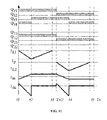
- the main waveform of rectifier mode is in the stable state as shown in the waveform diagram of FIG. 3 , where IL 1 and IL 2 are the current of first inductor 112 (L 1 ) and second inductor 124 (L 2 ), respectively, Im is the magnetizing current, and Idc is the secondary side current.
- the switch frequency is much higher than the frequency of Uac, so at any switching cycle, Uac may be considered as a constant voltage source.
- An analysis by timing stages is illustrated in the waveform diagram of FIG. 3 .
- Timing and operation of the one or more circuit diagrams disclosed in FIG. 2 is illustrated in FIGS. 4 through 9 in which each successive figure represents a successive time period and the bolded portion of the circuit indicates current flow.
- the second switch 154 (Qr 2 ) is kept turned off, and the third bi-directional switch 130 (Q 12 ), the first switch 152 (Qr 1 ), and the third switch 156 (Qr 3 ) turns on.
- the current in the first inductor 112 (L 1 ) increases from zero.
- the third bi-directional switch 130 (Q 12 ) turns on in zero current state (ZCS) and first switch 152 (Qr 1 ) turns on in zero voltage state (ZVS).
- the waveform diagram of FIG. 3 illustrates respective current flows at time 1 (t 1 ).
- the third switch 156 (Qr 3 ) turns off, and the fourth switch 160 (Qr 4 ) turns on.
- the current from the third switch 156 (Qr 3 ) changes to the inner diode of the fourth switch 160 (Qr 4 ).
- the fourth switch 160 (Qr 4 ) turns on with ZVS.
- the waveform diagram of FIG. 3 illustrates respective current flows at time 2 (t 2 ).
- the current in the primary side decreases to zero, so the third bi-directional switch 130 (Q 12 ) turns off in ZCS.
- the Udc provides the magnetizing current, so DC current (Idc) is negative.
- the waveform diagram of FIG. 3 illustrates respective current flows at time 3 (t 3 ).
- the fourth bi-directional switch 132 (Q 22 ) turns on instead of the third bi-directional switch 130 (Q 12 ).
- This stage is similar to the stage illustrated in FIG. 4 .
- the waveform diagram of FIG. 3 illustrates respective current flows at time Ts/2 (Ts/2).
- the fourth bi-directional switch 132 (Q 22 ) turns on instead of the third bi-directional switch 130 (Q 12 ).
- the second switch 154 (Qr 2 ) and the fourth switch 160 (Qr 4 ) are conducting current instead of the first switch 152 (Qr 1 ) and third switch 156 (Qr 3 ).
- the second switch 154 (Qr 2 ) is turned on with ZVS.
- the converter 10 may also be operated in a rectifier mode.
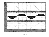
- FIG. 10 illustrates the rectifier mode voltage waveform, high-frequency current waveform and its waveform for the switching-cycle average value, and the filtered low-frequency current waveform of the AC source Uac if a passive LC filter is connected between the AC source and the AC input terminal of the AC-DC converter.
- the filtered low-frequency AC source current may be a sinusoidal waveform or a sinusoidal waveform with minor high-order harmonics.
- the main waveform of inverter mode is in the stable state as shown in FIG. 11 , where IL 1 and IL 2 are the current of first inductor 112 (L 1 ) and second inductor 124 (L 2 ), respectively, Im is the magnetizing current, and Idc is the secondary side current.
- the switch frequency is much higher than the frequency of Uac, so at any switching cycle Uac may be considered as a constant voltage source. From t 1 to t 2 , first switch 152 (Qr 1 ), fourth switch 160 (Qr 4 ), and first bi-directional switch 110 (Q 11 ) are turned on.
- the battery pack voltage is reflected to the primary side of the transformer 102 (T 1 ) as Ut 1 , which is larger than Uac.
- Ut 1 the current in first inductor 112 (L 1 ) starts to increase but the direction of the current is reversed compared to that in rectifier mode.
- the battery pack voltage is reflected to the primary side of the transformer as Ut 2 , which is larger than Uac.
- Ut 2 the current in the second inductor 124 (L 2 ) starts to increase but the direction of the current is reversed compared to that in rectifier mode.
- the fourth switch 160 Qr 4
- Ut 2 0 and the current in the second inductor 124 (L 2 ) starts to decrease and reach zero at t 5 .
- the corresponding magnetizing current (Im) and the battery pack current (Idc) waveforms are also shown in FIG. 11 .
- the zero voltage switching (ZVS) of the first switch 152 (Qr 1 ) and second switch 154 (Qr 2 ) is obtained by the magnetizing current at the instant of being switched on.
- the primary side switch 130 (Q 12 ) and second bi-directional switch 122 (Q 21 ) are turned off with zero current switching (ZCS).
- FIG. 12 illustrates the inverter mode voltage waveform, high-frequency current waveform and its waveform for the switching-cycle average value, and the filtered low-frequency current waveform of the AC source Uac if a passive LC filter is connected between the AC source and the AC input terminal of the AC-DC converter.
- the filtered low-frequency AC source current a sinusoidal waveform or a sinusoidal waveform with minor high-order harmonics.
- FIG. 13 illustrates one or more circuit diagrams disclosed herein for use as one or more AC-DC converters, generally designated 210 .
- the one or more circuits may include switches 212 (S 1 ), 214 (S 2 ), 216 (S 4 ), and 220 (S 5 ) on the primary side of the transformer 202 (T 1 ).
- Each of the switches 212 (S 1 ), 214 (S 2 ), 216 (S 4 ), and 220 (S 5 ) may be an IGBT, MOSFET, or a silicone controlled rectifier (SCR) switch.
- a first inductor 222 (L 1 ) and a second inductor 224 (L 2 ) may be provided.
- Inductor 222 (L 1 ) may be in series with switch 212 (S 1 ) and 214 (S 2 ). Inductor 224 (L 2 ) may be in series with switch 216 (S 4 ) and 220 (S 5 ).
- An LC filter may be provided between the AC source 236 (Uac) and the first switch 212 (S 1 ) that includes a capacitor 232 (Cin) and inductor 234 (Lin).
- Inductor 226 (C 1 ) and inductor 230 (C 2 ) may also be provided on the primary side.
- the primary side transformer windings 240 (T 1 ) and 242 (T 2 ) may be separated about transformer 202 (T 1 ) and connected in parallel as illustrated.
- a capacitor 250 (Co) On the secondary side is included a capacitor 250 (Co), a switch 252 (S 7 ), a switch 254 (S 8 ), a switch 256 (S 9 ), a switch 260 (S 10 ), and transformer winding 262 (T 3 ).
- a capacitor 250 (Co) On the secondary side is included a capacitor 250 (Co), a switch 252 (S 7 ), a switch 254 (S 8 ), a switch 256 (S 9 ), a switch 260 (S 10 ), and transformer winding 262 (T 3 ).
- the gate signals of corresponding switches (S 1 and S 4 , or S 2 and S 5 ) in the two basic structures are shifted 180 degrees in order to synthesize the high frequency AC current and voltage can pass through the transformer and prevent transformer core saturation.
- the first switch (S 1 or S 4 ) conducts in the first half cycle and a half-cycle series resonance is performed. At the end of the resonance, the energy is transferred from AC input to the resonant capacitor and the input switch is turned off with zero current which eliminates the switch turn-off loss. Then the second switch (S 2 or S 5 ) conducts in the second half cycle. With the coordination of semiconductor switches in the output stage, the other half-cycle series resonance is performed, which transfer the energy stored in the resonant capacitor to the DC output. At the end of the resonance, the second switch is turned off with zero current. Similar resonance operation occurs in the inverter mode, however, the second switch conducts firstly and the first switch conducts in the second half cycle in inverter mode operation. Zero current switching is obtained for the switches as well which eliminates turn-off loss.
- two basic structures are paralleled in the AC side and connected to two identical primary windings of the high frequency transformer in the other side.
- the gate signals of corresponding switches in the two basic structures arc shifted 180 degrees in order to synthesize the high frequency AC current and voltage which can pass through the transformer 202 (T 1 ) and prevent transformer core saturation.
- the output stage typically consists of a full bridge with the secondary side winding of high frequency transformer 202 (T 1 ) as the input.
- the phase-shift modulation is applied to the output full bridge such that the initial capacitor voltage of resonant capacitor can be controlled and so is the magnitude of the power flow.
- the invented converter may be relatively compact.
- the energy transfer process is based on resonance such that the semiconductor power devices switch at soft conditions in full load range thus increasing the power conversion efficiency of the converter.
- dv/dt and di/dt in the circuit is significantly reduced and EMI issues are mitigated.
- the one or more converters can also be used in three-phase applications with one converter for each phase.
- the switches paralleled with a capacitor are removed and the power is controlled by modulation of secondary full bridge which makes the operation of AC-DC converter simpler.
- the input stage can be built from some basic topological structures.
- one power semiconductor switch, one inductor and one capacitor build the first series resonant branch.
- the other power semiconductor switch and the other inductor build the second series resonant branch together with the same capacitor in the first series resonant branch.
- the inductor in the second series resonant branch can utilize the high frequency transformer leakage inductance and be integrated into the transformer.
- a third power semiconductor switch may be put in parallel with the resonant capacitor.
- the input stage can be built from various topological structures.
- one power semiconductor switch, one inductor and one capacitor build the first series resonant branch.
- the other power semiconductor switch and the other inductor build the second series resonant branch together with the same capacitor in the first series resonant branch.
- the inductor in the second series resonant branch can utilize the high frequency transformer leakage inductance and be integrated into the transformer.
- the turn-on and turn-off instant of the third power semiconductor switch is controlled such that the initial capacitor voltage of resonant capacitor can be controlled and so is the magnitude of the power flow.
- FIG. 14 illustrates one or more circuit diagrams disclosed herein for use as one or more AC-DC converters where the circuit is generally designated 310 .
- the one or more circuits 310 may include switches 312 (Q 1 ), 314 (Q 2 ), 316 (Q 3 ), and 320 (Q 4 ) on the primary side of the transformer 302 (T 1 ).
- Each of the switches may be an IBGT, MOSFET, or an SCR switch.
- a first inductor 322 (L 1 ) may be provided and may be in series with each of the switches.
- a primary side transformer winding 326 is provided, along with an AC source 324 (Uac).
- bi-directional switch 352 Qr 1
- bi-directional switch 354 Qr 2
- bi-directional switch 356 Qr 3
- bi-directional switch 360 Qr 4
- a DC source may be provided 350 (Udc), along with transformer winding 362 .
- the one or more circuits 410 may include switches 412 (Q 11 ), 413 (Q 12 ), 414 (Q 21 ), 415 (Q 22 ), 416 (Q 31 ), 417 (Q 32 ), 420 (Q 41 ), and 421 (Q 42 ) on the primary side of the transformer 402 (T 1 ).
- Each of the switches may be an IBGT, MOSFET, or an SCR switch.
- a first inductor 422 (L 1 ) may be provided and may be in series with each of the switches.
- a primary side transformer winding 426 is provided, along with an AC source 424 (Uac).
- bi-directional switch 452 Qr 1
- bi-directional switch 454 Qr 2
- bi-directional switch 456 Qr 3
- bi-directional switch 460 Qr 4
- a current source may be provided 450 (U 0 ), along with transformer winding 462 .
- FIGS. 16 through 19 Timing and operation of the one or more circuit diagrams disclosed in FIG. 16 in rectifier mode is illustrated in FIGS. 16 through 19 in which each successive figure represents a successive time period and the bolded portion of the circuit indicates current flow.
- input voltage is applied to the inductor 422 (L 1 ).
- the secondary side of the transformer 402 (T 1 ) is short-circuited.
- the current increases from zero, and switch 412 (Q 11 ) and switch 420 (Q 41 ) ZCS turn on.
- switch 456 (Qr 3 ) turns off, and this may be a hard switch.
- Switch 460 (Qr 4 ) is turned on with ZVS. The input voltage and output voltage are applied to inductor 422 (L 1 ) together. The current decreases to zero. The magnetizing current increases.
- the current It 1 is zero and the magnetizing current is provided by Uo and passes through first switch 452 (Qr 1 ) and switch 460 (Qr 4 ).
- switch 412 (Q 11 ), switch 420 (Q 41 ), and switch 452 (Qr 1 ) are turned off.
- switch 415 (Q 22 ), switch 417 (Q 32 ), and switch 454 (Qr 2 ) are turned on.
- switch 454 (Qr 2 ) ZVS turns on.
- Switch 415 (Q 22 ) and switch 417 (Q 32 ) turn on with ZCS.
- FIG. 20 Timing and operation of the one or more circuit diagrams disclosed in FIG. 16 in inverter mode is illustrated in FIG. 20 .
- the one or more transformer isolated soft switched single-stage AC-DC converters disclosed herein are more compact than conventional AC-DC-DC converters with a PWM rectifier stage and isolation transformer because there is no DC-link capacitor bank, a fewer number of semiconductor switches, and smaller heat sinks.
- the semiconductor power devices are switched at soft conditions in the full load range which greatly reduces the switching loss and improves the converter efficiency compared to conventional hard-switched PWM rectifier. Due to the resonance operation of the circuit, di/dt and AC point of connection, dv/dt are significantly reduced as well as electromagnetic interference (EMI). Higher switching frequency can be selected due to the soft switching and then a smaller input filter can be used. The input current harmonic may be very low ( ⁇ 2%).
- the galvanic isolation and high voltage gain can be obtained by the integrated high frequency transformer in the converter.
- the one or more converters disclosed herein have many commercial applications. For example, the one or more converters can be used in most of the applications where the conventional PWM AC-DC converters arc used. Additionally, the one or more converters may be advantageous in applications which require galvanic isolation or high voltage gain.
- One typical application may be the PHEV (plug-in hybrid electric vehicle) or EV (electric vehicle) onboard battery pack charger. The charger is mounted on the vehicle and high power density is required.
- the one or more converters disclosed herein utilize a high frequency transformer that provides more safe galvanic isolation between the grid and vehicle and may accommodate any voltage difference between the pack terminal voltage and grid voltage.
- the low power loss associated with the one or more embodiments disclosed herein provide for efficient energy transfer for both charging and discharging vehicle-to-grid (V2G) mode of the battery.
- V2G vehicle-to-grid
- the one or more converters disclosed herein may be appropriately configured for use as one or more solid state transformers.
- the efficiency of the one or more solid state transformers will be increased compared to the traditional topology used for solid state transformer applications and may be close to the very high efficient line frequency transformer. Additionally, the volume and weight of the transformer will be much lower since it operates at high frequency. In addition the high dv/dt and di/dt issues which are typically severe in high voltage and high frequency converters will be greatly mitigated.
- higher voltage rating devices or series connection of devices may be employed for the semiconductor power switches. This disadvantage can be solved by back-to-back connection of two IGCTs or MOSFETs and package them together in mass production.
- there are multiple approaches to control the power or input current include the turn-off instant of switches, phase-shift modulation of a secondary full bridge, and switching frequency. Additionally, power can be transferred to the secondary side during the extremely low input voltage period of an AC cycle.
- the first switch conducts in the first half cycle and a half-cycle series resonance is performed. At the end of the resonance, the energy is transferred from AC input to the resonant capacitor and the input switch is turned off with zero current which eliminates the switch turn-off loss. Then the second switch of the basic structure conducts in the second half cycle. With the coordination of semiconductor switches in the output stage, the other half-cycle series resonance is performed, which transfer the energy stored in the resonant capacitor to the DC output. At the end of the resonance, the second switch is turned off with zero current. Similar resonance operation may occur in the inverter mode, however, the second switch conducts firstly and the first switch conducts in the second half cycle in inverter mode operation. Zero current switching is obtained for the two switches as well which eliminates turn-off loss.
- the phase-shift modulation is applied to the output full bridge such that the initial capacitor voltage of resonant capacitor can be controlled and so is the magnitude of the power flow.
- the switching frequency is adjusted such that the frequency of transfer energy from input to output or from output to input is controlled as is the magnitude of the power flow.
- bidirectional four-quadrant semiconductor power switches can be replaced by voltage bi-directional two-quadrant semiconductor power switches for uni-directional power conversion applications.
- both input and output are DC and the invented converter can be used as DC-DC converter.
- both input and output are AC and the invented converter can be used as AC-AC converter.
- the input of three AC-DC converters are connected to three-phase AC input and the output are parallel connected and it can be used as three-phase AC-DC converter.
Landscapes
- Engineering & Computer Science (AREA)
- Power Engineering (AREA)
- Dc-Dc Converters (AREA)
Abstract
Description
Claims (18)
Priority Applications (1)
| Application Number | Priority Date | Filing Date | Title |
|---|---|---|---|
| US13/595,883 US8861238B2 (en) | 2011-08-25 | 2012-08-27 | Isolated soft-switch single-stage AC-DC converter |
Applications Claiming Priority (2)
| Application Number | Priority Date | Filing Date | Title |
|---|---|---|---|
| US201161527411P | 2011-08-25 | 2011-08-25 | |
| US13/595,883 US8861238B2 (en) | 2011-08-25 | 2012-08-27 | Isolated soft-switch single-stage AC-DC converter |
Publications (2)
| Publication Number | Publication Date |
|---|---|
| US20130051102A1 US20130051102A1 (en) | 2013-02-28 |
| US8861238B2 true US8861238B2 (en) | 2014-10-14 |
Family
ID=47743537
Family Applications (1)
| Application Number | Title | Priority Date | Filing Date |
|---|---|---|---|
| US13/595,883 Active US8861238B2 (en) | 2011-08-25 | 2012-08-27 | Isolated soft-switch single-stage AC-DC converter |
Country Status (1)
| Country | Link |
|---|---|
| US (1) | US8861238B2 (en) |
Cited By (12)
| Publication number | Priority date | Publication date | Assignee | Title |
|---|---|---|---|---|
| US20140112043A1 (en) * | 2011-07-04 | 2014-04-24 | Panasonic Corporation | Switching power supply apparatus |
| US20150263605A1 (en) * | 2014-03-14 | 2015-09-17 | Delta-Q Technologies Corp. | Hybrid resonant bridgeless ac-dc power factor correction converter |
| US20150295442A1 (en) * | 2014-04-11 | 2015-10-15 | Primus Power Corporation | Series-connected storage interface converter |
| USD815592S1 (en) | 2016-05-18 | 2018-04-17 | Delta-Q Technologies Corp. | Battery charger |
| USD828294S1 (en) | 2015-06-12 | 2018-09-11 | Delta-Q Technologies Corp. | Battery charger |
| USD829649S1 (en) | 2015-08-11 | 2018-10-02 | Delta-Q Technologies Corp. | Battery charger |
| USD854497S1 (en) | 2016-12-05 | 2019-07-23 | Delta-Q Technologies Corp. | Battery charger |
| US10720787B2 (en) | 2017-07-26 | 2020-07-21 | Delta-Q Technologies Corp. | Combined charger and power converter |
| US10879813B2 (en) | 2018-09-21 | 2020-12-29 | Delta-Q Technologies Corp. | Bridgeless single-stage AC/DC converter |
| USD1004541S1 (en) | 2020-05-05 | 2023-11-14 | Delta-Q Technologies Corp. | Battery charger |
| USD1022880S1 (en) | 2021-11-29 | 2024-04-16 | Delta-Q Technologies Corp. | Battery charger |
| WO2024192511A1 (en) * | 2023-03-17 | 2024-09-26 | The Governors of the University of Alberta | Beat frequency modulated single-stage soft-switched microinverter |
Families Citing this family (33)
| Publication number | Priority date | Publication date | Assignee | Title |
|---|---|---|---|---|
| JP5768886B2 (en) * | 2011-08-04 | 2015-08-26 | 株式会社村田製作所 | Switching power supply |
| TWM438653U (en) * | 2012-05-24 | 2012-10-01 | Shi Jie Magnetic Energy Co Ltd | Single phase reactance power saving device |
| CN102832826B (en) * | 2012-08-24 | 2016-01-27 | 台达电子工业股份有限公司 | For the control circuit of power inverter, transformation system and control method thereof |
| NL2011825C2 (en) * | 2013-11-21 | 2015-05-26 | Univ Eindhoven Tech | Single-stage isolated bi-directional ac/dc converter. |
| US9871450B2 (en) * | 2016-04-25 | 2018-01-16 | Vanner, Inc. | Isolated step-up converter |
| US11201548B2 (en) * | 2016-12-15 | 2021-12-14 | Foundation For Research And Business, Seoul National University Of Science And Technology | Single-stage interleaved soft switching converter |
| FR3061818B1 (en) * | 2017-01-10 | 2019-05-31 | Commissariat A L'energie Atomique Et Aux Energies Alternatives | AC-DC POWER CONVERTER |
| US10193462B1 (en) * | 2017-10-11 | 2019-01-29 | Infineon Technologies Ag | Power converter using bi-directional active rectifying bridge |
| US10819336B2 (en) | 2017-12-28 | 2020-10-27 | Intelesol, Llc | Electronic switch and dimmer |
| JP7089377B2 (en) * | 2018-03-02 | 2022-06-22 | 株式会社豊田中央研究所 | Power converter |
| US11671029B2 (en) | 2018-07-07 | 2023-06-06 | Intelesol, Llc | AC to DC converters |
| US11581725B2 (en) | 2018-07-07 | 2023-02-14 | Intelesol, Llc | Solid-state power interrupters |
| US11056981B2 (en) | 2018-07-07 | 2021-07-06 | Intelesol, Llc | Method and apparatus for signal extraction with sample and hold and release |
| US11334388B2 (en) | 2018-09-27 | 2022-05-17 | Amber Solutions, Inc. | Infrastructure support to enhance resource-constrained device capabilities |
| US11205011B2 (en) | 2018-09-27 | 2021-12-21 | Amber Solutions, Inc. | Privacy and the management of permissions |
| US11349296B2 (en) | 2018-10-01 | 2022-05-31 | Intelesol, Llc | Solid-state circuit interrupters |
| US10985548B2 (en) | 2018-10-01 | 2021-04-20 | Intelesol, Llc | Circuit interrupter with optical connection |
| US10483862B1 (en) | 2018-10-25 | 2019-11-19 | Vanner, Inc. | Bi-directional isolated DC-DC converter for the electrification of transportation |
| DE112018004240T5 (en) * | 2018-12-17 | 2021-04-08 | Fuji Electric Co., Ltd. | DC-DC CONVERTER |
| EP3900487A4 (en) | 2018-12-17 | 2022-09-21 | Intelesol, LLC | Ac-driven light-emitting diode systems |
| US11373831B2 (en) | 2019-05-18 | 2022-06-28 | Amber Solutions, Inc. | Intelligent circuit breakers |
| US11152918B1 (en) * | 2019-10-16 | 2021-10-19 | National Technology & Engineering Solutions Of Sandia, Llc | Low modulation index 3-phase solid state transformer |
| CN111064369A (en) * | 2019-12-20 | 2020-04-24 | 矽力杰半导体技术(杭州)有限公司 | Switching power supply circuit |
| JP7554272B2 (en) | 2020-01-21 | 2024-09-19 | アンバー セミコンダクター,インク. | Intelligent Circuit Breaker |
| CN113942403B (en) * | 2020-06-30 | 2023-08-08 | 比亚迪股份有限公司 | Electric vehicle, charge-discharge device, and control method therefor |
| KR102387123B1 (en) * | 2020-07-21 | 2022-04-15 | 한국항공우주연구원 | Ac-dc converter circuit system, and operating method of ac-dc converter circuit system |
| EP4107849A4 (en) * | 2020-08-05 | 2023-11-08 | Amber Semiconductor, Inc. | Two-wire electronic switch and dimmer |
| EP4197086A4 (en) | 2020-08-11 | 2024-09-04 | Amber Semiconductor Inc | Intelligent energy source monitoring and selection control system |
| CN112448388B (en) * | 2020-11-04 | 2022-02-22 | 南方电网科学研究院有限责任公司 | Control method of power conversion and supply system based on parallel connection of intelligent soft switch and interconnection switch |
| DE102021103205A1 (en) | 2021-02-11 | 2022-08-11 | Bayerische Motoren Werke Aktiengesellschaft | Supplying electrical energy from an AC voltage network to a DC voltage network |
| US11239846B1 (en) * | 2021-06-01 | 2022-02-01 | SambaNova Systems, Inc. | Variable-length clock stretcher with correction for glitches due to phase detector offset |
| US12113525B2 (en) | 2021-09-30 | 2024-10-08 | Amber Semiconductor, Inc. | Intelligent electrical switches |
| CN116937941B (en) * | 2023-07-27 | 2024-03-26 | 深圳市英可瑞数字能源技术有限公司 | Three-phase single-stage isolated AC/DC converter and control method thereof |
Citations (12)
| Publication number | Priority date | Publication date | Assignee | Title |
|---|---|---|---|---|
| US5705923A (en) * | 1992-03-13 | 1998-01-06 | Bha Group, Inc. | Variable inductance current limiting reactor control system for electrostatic precipitator |
| US6067243A (en) * | 1996-06-06 | 2000-05-23 | I-Hits Laboratory Corporation | AC-AC/DC converter |
| US6118673A (en) * | 1998-06-01 | 2000-09-12 | Virginia Power Technologies, Inc. | Single-stage AC/DC converters with saturable conductor PFC |
| US6366474B1 (en) * | 2000-09-29 | 2002-04-02 | Jeff Gucyski | Switching power supplies incorporating power factor correction and/or switching at resonant transition |
| US6606257B2 (en) * | 2001-11-05 | 2003-08-12 | Koninklijke Philips Electronics N.V. | Independent regulation of multiple outputs in a soft-switching multiple-output flyback converter |
| US6784644B2 (en) * | 2001-02-22 | 2004-08-31 | Virginia Tech Intellectual Properties, Inc. | Multiphase clamp coupled-buck converter and magnetic integration |
| US7164589B1 (en) * | 2005-07-11 | 2007-01-16 | International Rectifier Corporation | Bridgeless bi-directional forward type converter |
| US20080130339A1 (en) * | 2006-11-30 | 2008-06-05 | Dell Products L.P. | Apparatus and Methods for Power Conversion |
| US20090040800A1 (en) * | 2007-08-10 | 2009-02-12 | Maximiliano Sonnaillon | Three phase rectifier and rectification method |
| US20110031927A1 (en) * | 2009-08-05 | 2011-02-10 | Gm Global Technology Operations, Inc. | Charging system with galvanic isolation and multiple operating modes |
| US20110115285A1 (en) * | 2009-11-19 | 2011-05-19 | Gm Global Technology Operations, Inc. | Systems and methods for commutating inductor current using a matrix converter |
| US20110149610A1 (en) * | 2009-12-21 | 2011-06-23 | Intersil Americas Inc. | Bidirectional signal conversion |
-
2012
- 2012-08-27 US US13/595,883 patent/US8861238B2/en active Active
Patent Citations (12)
| Publication number | Priority date | Publication date | Assignee | Title |
|---|---|---|---|---|
| US5705923A (en) * | 1992-03-13 | 1998-01-06 | Bha Group, Inc. | Variable inductance current limiting reactor control system for electrostatic precipitator |
| US6067243A (en) * | 1996-06-06 | 2000-05-23 | I-Hits Laboratory Corporation | AC-AC/DC converter |
| US6118673A (en) * | 1998-06-01 | 2000-09-12 | Virginia Power Technologies, Inc. | Single-stage AC/DC converters with saturable conductor PFC |
| US6366474B1 (en) * | 2000-09-29 | 2002-04-02 | Jeff Gucyski | Switching power supplies incorporating power factor correction and/or switching at resonant transition |
| US6784644B2 (en) * | 2001-02-22 | 2004-08-31 | Virginia Tech Intellectual Properties, Inc. | Multiphase clamp coupled-buck converter and magnetic integration |
| US6606257B2 (en) * | 2001-11-05 | 2003-08-12 | Koninklijke Philips Electronics N.V. | Independent regulation of multiple outputs in a soft-switching multiple-output flyback converter |
| US7164589B1 (en) * | 2005-07-11 | 2007-01-16 | International Rectifier Corporation | Bridgeless bi-directional forward type converter |
| US20080130339A1 (en) * | 2006-11-30 | 2008-06-05 | Dell Products L.P. | Apparatus and Methods for Power Conversion |
| US20090040800A1 (en) * | 2007-08-10 | 2009-02-12 | Maximiliano Sonnaillon | Three phase rectifier and rectification method |
| US20110031927A1 (en) * | 2009-08-05 | 2011-02-10 | Gm Global Technology Operations, Inc. | Charging system with galvanic isolation and multiple operating modes |
| US20110115285A1 (en) * | 2009-11-19 | 2011-05-19 | Gm Global Technology Operations, Inc. | Systems and methods for commutating inductor current using a matrix converter |
| US20110149610A1 (en) * | 2009-12-21 | 2011-06-23 | Intersil Americas Inc. | Bidirectional signal conversion |
Non-Patent Citations (4)
| Title |
|---|
| Conference Paper from Nov. 15, 2010 conference held at the FREEDM Systems Center, NCSU, Transformer-Isolated Soft-switched Single-stage AC-DC Converter. |
| Du, Yu et al., High-frequency High-efficiency DC-DC Converter for Distributed Energy Storage Modularization, IEEE, IECON 2010 36th Annual Conference, Nov. 7-10, 2010, p. 1832-1837 and the Second FREEDM Systems annual conference, May 18-20, 2010. |
| Falcones S., Mao X., Ayyanar R.; Topology Comparison for Solid State Transformer Implementation; Jul. 2010; IEEE, pp. 1-8. |
| Related U.S. Appl. No. 13/600,280, filed Aug. 31, 2012; not yet public. |
Cited By (17)
| Publication number | Priority date | Publication date | Assignee | Title |
|---|---|---|---|---|
| US9318971B2 (en) * | 2011-07-04 | 2016-04-19 | Panasonic Intellectual Property Management Co., Ltd. | Switching power supply apparatus |
| US20140112043A1 (en) * | 2011-07-04 | 2014-04-24 | Panasonic Corporation | Switching power supply apparatus |
| US20150263605A1 (en) * | 2014-03-14 | 2015-09-17 | Delta-Q Technologies Corp. | Hybrid resonant bridgeless ac-dc power factor correction converter |
| US9490694B2 (en) * | 2014-03-14 | 2016-11-08 | Delta-Q Technologies Corp. | Hybrid resonant bridgeless AC-DC power factor correction converter |
| US20150295442A1 (en) * | 2014-04-11 | 2015-10-15 | Primus Power Corporation | Series-connected storage interface converter |
| US9577454B2 (en) * | 2014-04-11 | 2017-02-21 | Primus Power Corporation | Series connected storage interface converter |
| USD828294S1 (en) | 2015-06-12 | 2018-09-11 | Delta-Q Technologies Corp. | Battery charger |
| USD829649S1 (en) | 2015-08-11 | 2018-10-02 | Delta-Q Technologies Corp. | Battery charger |
| USD815592S1 (en) | 2016-05-18 | 2018-04-17 | Delta-Q Technologies Corp. | Battery charger |
| USD853956S1 (en) | 2016-05-18 | 2019-07-16 | Delta-Q Technologies Corp. | Battery charger |
| USD854497S1 (en) | 2016-12-05 | 2019-07-23 | Delta-Q Technologies Corp. | Battery charger |
| USD884612S1 (en) | 2016-12-05 | 2020-05-19 | Delta-Q Technologies Corp. | Battery charger |
| US10720787B2 (en) | 2017-07-26 | 2020-07-21 | Delta-Q Technologies Corp. | Combined charger and power converter |
| US10879813B2 (en) | 2018-09-21 | 2020-12-29 | Delta-Q Technologies Corp. | Bridgeless single-stage AC/DC converter |
| USD1004541S1 (en) | 2020-05-05 | 2023-11-14 | Delta-Q Technologies Corp. | Battery charger |
| USD1022880S1 (en) | 2021-11-29 | 2024-04-16 | Delta-Q Technologies Corp. | Battery charger |
| WO2024192511A1 (en) * | 2023-03-17 | 2024-09-26 | The Governors of the University of Alberta | Beat frequency modulated single-stage soft-switched microinverter |
Also Published As
| Publication number | Publication date |
|---|---|
| US20130051102A1 (en) | 2013-02-28 |
Similar Documents
| Publication | Publication Date | Title |
|---|---|---|
| US8861238B2 (en) | Isolated soft-switch single-stage AC-DC converter | |
| Zinchenko et al. | High-efficiency single-stage on-board charger for electrical vehicles | |
| US11962235B2 (en) | Modular multi-level DC/DC converter with current-shaping | |
| CN104300771B (en) | Universal power converter | |
| Shang et al. | Design and analysis of a high-voltage-gain step-up resonant DC–DC converter for transportation applications | |
| CN112970182A (en) | AC-DC three-level conversion system with high-frequency intermediate AC and two independent outputs | |
| Mozaffari et al. | A highly reliable and efficient class of single-stage high-frequency AC-link converters | |
| Lee et al. | A single-phase battery charger design for LEV based on DC-SRC with resonant valley-fill circuit | |
| Ramakrishnan et al. | Power topology considerations for electric vehicle charging stations | |
| Nasr et al. | SiC based on-board EV power-hub with high-efficiency DC transfer mode through AC port for vehicle-to-vehicle charging | |
| Abbasi et al. | An interleaved bridgeless single-stage AC/DC converter with stacked switches configurations and soft-switching operation for high-voltage EV battery systems | |
| Xu et al. | Soft-switching current-source rectifier based onboard charging system for electric vehicles | |
| Aarninkhof et al. | A Reconfigurable Two-Stage 11 kW DC–DC Resonant Converter for EV Charging With a 150–1000 V Output Voltage Range | |
| Mishima et al. | A Single-Stage High-Frequency-Link Modular Three-Phase $ LLC $ AC–DC Converter | |
| Tian et al. | Widen the zero-voltage-switching range and secure grid power quality for an ev charger using variable-switching-frequency single-dual-phase-shift control | |
| Asa et al. | A novel ac to ac wireless power transfer system for EV charging applications | |
| Patel et al. | A Soft-Switched Single-Stage Single-Phase PFC Converter for Bidirectional Plug-In EV Charger | |
| Sabi et al. | Design and implementation of a bipolar-unipolar switched boundary current mode (BCM) control GaN-based single-phase inverter | |
| WO2024187553A1 (en) | Single-stage three-port magnetic integrated topology, and vehicle-mounted charger and control method therefor | |
| TWI794329B (en) | Dc-to-ac power converter and isolated dc-to-dc converter suitable to be used in the dc-to-ac power converter | |
| Bolte et al. | Bidirectional resonant converter with integrated magnetics for on-board chargers | |
| Pan et al. | Electrolytic capacitorless current-fed single-phase pulsating DC link inverter | |
| Stanojević et al. | Comparison of 2-stage isolated converters for fast EV charger, using partial power | |
| Patel et al. | An Accurate Loss Model of Single-Stage Single-Phase Isolated PFC Converter for Bidirectional Plug-in EV Charger | |
| US20230322105A1 (en) | Charging device and method for operating the charging device |
Legal Events
| Date | Code | Title | Description |
|---|---|---|---|
| AS | Assignment |
Owner name: NORTH CAROLINA STATE UNIVERSITY, NORTH CAROLINA Free format text: ASSIGNMENT OF ASSIGNORS INTEREST;ASSIGNORS:HUANG, QIN;DU, YU;YAO, WENXI;REEL/FRAME:028890/0883 Effective date: 20120822 |
|
| STCF | Information on status: patent grant |
Free format text: PATENTED CASE |
|
| CC | Certificate of correction | ||
| AS | Assignment |
Owner name: NATIONAL SCIENCE FOUNDATION, VIRGINIA Free format text: CONFIRMATORY LICENSE;ASSIGNOR:NORTH CAROLINA STATE UNIVERSITY, RALEIGH;REEL/FRAME:044255/0476 Effective date: 20171012 |
|
| MAFP | Maintenance fee payment |
Free format text: PAYMENT OF MAINTENANCE FEE, 4TH YR, SMALL ENTITY (ORIGINAL EVENT CODE: M2551) Year of fee payment: 4 |
|
| MAFP | Maintenance fee payment |
Free format text: PAYMENT OF MAINTENANCE FEE, 8TH YR, SMALL ENTITY (ORIGINAL EVENT CODE: M2552); ENTITY STATUS OF PATENT OWNER: SMALL ENTITY Year of fee payment: 8 |
|
| AS | Assignment |
Owner name: PNC BANK, NATIONAL ASSOCIATION, PENNSYLVANIA Free format text: SECURITY INTEREST;ASSIGNORS:ERMCO COMPONENTS, INC.;GRIDBRIDGE, INC.;JEFFERSON ELECTRIC LLC;REEL/FRAME:062105/0942 Effective date: 20221215 |