EP0903792A2 - Procédé pour la réalisation d'une pluralité de corps semi-conducteurs - Google Patents
Procédé pour la réalisation d'une pluralité de corps semi-conducteurs Download PDFInfo
- Publication number
- EP0903792A2 EP0903792A2 EP98117796A EP98117796A EP0903792A2 EP 0903792 A2 EP0903792 A2 EP 0903792A2 EP 98117796 A EP98117796 A EP 98117796A EP 98117796 A EP98117796 A EP 98117796A EP 0903792 A2 EP0903792 A2 EP 0903792A2
- Authority
- EP
- European Patent Office
- Prior art keywords
- semiconductor
- windows
- wafer
- structures
- chips
- Prior art date
- Legal status (The legal status is an assumption and is not a legal conclusion. Google has not performed a legal analysis and makes no representation as to the accuracy of the status listed.)
- Granted
Links
- 239000004065 semiconductor Substances 0.000 title claims abstract description 98
- 238000004519 manufacturing process Methods 0.000 title claims description 19
- 238000000034 method Methods 0.000 claims description 60
- 239000000758 substrate Substances 0.000 claims description 53
- 229910052782 aluminium Inorganic materials 0.000 claims description 28
- 229910052738 indium Inorganic materials 0.000 claims description 27
- 239000000463 material Substances 0.000 claims description 20
- 238000005530 etching Methods 0.000 claims description 16
- 229910004298 SiO 2 Inorganic materials 0.000 claims description 5
- 238000001312 dry etching Methods 0.000 claims description 5
- 229910052594 sapphire Inorganic materials 0.000 claims description 5
- 239000010980 sapphire Substances 0.000 claims description 5
- 238000003631 wet chemical etching Methods 0.000 claims description 5
- 229910001218 Gallium arsenide Inorganic materials 0.000 claims description 2
- 238000000151 deposition Methods 0.000 abstract description 8
- 230000000873 masking effect Effects 0.000 abstract 1
- 235000012431 wafers Nutrition 0.000 description 38
- 238000001465 metallisation Methods 0.000 description 11
- 238000000407 epitaxy Methods 0.000 description 10
- 239000013078 crystal Substances 0.000 description 8
- 230000008021 deposition Effects 0.000 description 7
- 238000003486 chemical etching Methods 0.000 description 5
- 230000007547 defect Effects 0.000 description 5
- 238000005516 engineering process Methods 0.000 description 5
- 239000000126 substance Substances 0.000 description 4
- 150000001875 compounds Chemical class 0.000 description 2
- 229910052733 gallium Inorganic materials 0.000 description 2
- 230000002045 lasting effect Effects 0.000 description 2
- 229920002120 photoresistant polymer Polymers 0.000 description 2
- 238000000927 vapour-phase epitaxy Methods 0.000 description 2
- 238000001039 wet etching Methods 0.000 description 2
- 229910002704 AlGaN Inorganic materials 0.000 description 1
- 208000031872 Body Remains Diseases 0.000 description 1
- 241000951490 Hylocharis chrysura Species 0.000 description 1
- 239000003795 chemical substances by application Substances 0.000 description 1
- 238000005253 cladding Methods 0.000 description 1
- 238000011161 development Methods 0.000 description 1
- 230000018109 developmental process Effects 0.000 description 1
- 238000004020 luminiscence type Methods 0.000 description 1
- 239000002184 metal Substances 0.000 description 1
- 229910052751 metal Inorganic materials 0.000 description 1
- 239000000203 mixture Substances 0.000 description 1
- 150000004767 nitrides Chemical class 0.000 description 1
- 125000002524 organometallic group Chemical group 0.000 description 1
- 238000001259 photo etching Methods 0.000 description 1
Images


Classifications
-
- H—ELECTRICITY
- H01—ELECTRIC ELEMENTS
- H01S—DEVICES USING THE PROCESS OF LIGHT AMPLIFICATION BY STIMULATED EMISSION OF RADIATION [LASER] TO AMPLIFY OR GENERATE LIGHT; DEVICES USING STIMULATED EMISSION OF ELECTROMAGNETIC RADIATION IN WAVE RANGES OTHER THAN OPTICAL
- H01S5/00—Semiconductor lasers
- H01S5/02—Structural details or components not essential to laser action
- H01S5/0201—Separation of the wafer into individual elements, e.g. by dicing, cleaving, etching or directly during growth
-
- H—ELECTRICITY
- H10—SEMICONDUCTOR DEVICES; ELECTRIC SOLID-STATE DEVICES NOT OTHERWISE PROVIDED FOR
- H10H—INORGANIC LIGHT-EMITTING SEMICONDUCTOR DEVICES HAVING POTENTIAL BARRIERS
- H10H20/00—Individual inorganic light-emitting semiconductor devices having potential barriers, e.g. light-emitting diodes [LED]
- H10H20/01—Manufacture or treatment
- H10H20/011—Manufacture or treatment of bodies, e.g. forming semiconductor layers
- H10H20/013—Manufacture or treatment of bodies, e.g. forming semiconductor layers having light-emitting regions comprising only Group III-V materials
- H10H20/0133—Manufacture or treatment of bodies, e.g. forming semiconductor layers having light-emitting regions comprising only Group III-V materials with a substrate not being Group III-V materials
- H10H20/01335—Manufacture or treatment of bodies, e.g. forming semiconductor layers having light-emitting regions comprising only Group III-V materials with a substrate not being Group III-V materials the light-emitting regions comprising nitride materials
-
- H—ELECTRICITY
- H10—SEMICONDUCTOR DEVICES; ELECTRIC SOLID-STATE DEVICES NOT OTHERWISE PROVIDED FOR
- H10H—INORGANIC LIGHT-EMITTING SEMICONDUCTOR DEVICES HAVING POTENTIAL BARRIERS
- H10H20/00—Individual inorganic light-emitting semiconductor devices having potential barriers, e.g. light-emitting diodes [LED]
- H10H20/01—Manufacture or treatment
- H10H20/011—Manufacture or treatment of bodies, e.g. forming semiconductor layers
- H10H20/013—Manufacture or treatment of bodies, e.g. forming semiconductor layers having light-emitting regions comprising only Group III-V materials
- H10H20/0137—Manufacture or treatment of bodies, e.g. forming semiconductor layers having light-emitting regions comprising only Group III-V materials the light-emitting regions comprising nitride materials
Definitions
- the invention relates to a method for manufacturing a plurality of semiconductor bodies, in particular of radiation-emitting semiconductor bodies, according to the Preamble of claim 1.
- Luminescent diode chips are, for example, on a Semiconductor substrate wafer an electroluminescent Semiconductor layer sequence grew epitaxially. This so-called epi-wafer is subsequently after it with the required contact metallizations for electrical Contacting of the luminescence diode chips is provided, cut into luminescent diode chips by sawing. Similar Methods are used with transistor, IC chips, etc.
- EP 0 599 224 A1 describes a method in which a plurality of In x Ga 1-x N layers are epitaxially deposited on a substrate. This plurality of In x Ga 1-x N layers form a light-emitting diode (LED) layer sequence which extends over the entire wafer. After the deposition of the LED layer sequence, its structuring by means of etching and the application of a plurality of contact metallizations, the wafer is separated into a plurality of individual light-emitting diode chips by severing the wafer between the contact metallizations, for example by means of saws.
- LED light-emitting diode
- Ga (In, Al) N light-emitting diode structures When Ga (In, Al) N light-emitting diode structures are deposited, there is the particular problem of widely differing lattice constants of the nitrides to the corresponding substrates, regardless of the substrate material. A further difficulty is the very different thermal expansion coefficients of the available substrate materials (e.g. sapphire or SiC) and the system Ga (In, Al) N. The different thermal expansions caused by this cause that when the wafer is cooled from the Growth temperature to room temperature in the wafer thermally induced stresses occur. This leads to defects in the semiconductor structures, primarily Cracks ", holes etc., which have a lasting effect on the component properties such as ESD stability, service life etc. Under Ga (In, Al) N, Ga 1-xy In x Al y N with 0 ⁇ x ⁇ 1, 0 ⁇ y ⁇ 1 and x + y ⁇ 1 to understand.
- Ga (In, Al) N light emitting diode structures Another problem with Ga (In, Al) N light emitting diode structures occurs, is that this material system is chemically very stable. This property throws great Problems with component structuring. Structuring of the Ga (In, Al) N layer sequences on the wafer are only by means of technically complex methods such as Dry etching or UV-assisted wet chemical Etching process, possible.
- sapphire and GaN can be used because of their sawed hardness only with great technical effort become.
- the Laser mirror for example, the laser diode structures having epi semiconductor wafer according to the cleaved crystallographic directions of the substrate.
- the object of the present invention is a Procedure of the type mentioned to indicate that it allows, even when using mechanical and chemically very stable semiconductor materials and / or of Substrate and epitaxial layer materials with strong different lattice constants in a simple way a plurality of semiconductor bodies with precisely defined Side faces and / or reduced crystal disturbances to manufacture.
- the first step is preferably to Applied a highly etchable mask layer, the substrate wafer subsequently, for example, using a photo technology
- a plurality of mask openings (windows) is provided in which the main surface of the substrate wafer is exposed.
- the semiconductor layer sequence of Light emitting diode structures or semiconductor laser structures in the windows on the main surface of the substrate wafer deposited.
- the windows define the lateral Shape of the semiconductor layer sequence.
- a dielectric layer made of SiO 2 or Si x N 1-x is advantageously used as the mask layer and the windows are produced, for example, by means of an isotropic wet chemical etching process (e.g. using a conventional window etching solution) or by means of a dry chemical etching process, which is preferably selective with respect to the substrate material .
- the method is particularly preferred for semiconductor bodies used in which the substrate made of SiC, sapphire or GaN exists and in which the semiconductor layer sequence at least a semiconductor layer made of the Ga (In, Al) N material system having.
- semiconductor laser structures or semiconductor laser structures for example edge-emitting laser diodes and VCSEL (Vertical Cavity Surface Emitting Laser) diodes
- GaN-based III-V compound semiconductors such as Ga 1-xy In x Al y N with 0 ⁇ x ⁇ 1, 0 ⁇ y ⁇ 1 and x + y ⁇ 1, because the problems mentioned at the outset are particularly important here.
- the laser mirrors are used in the invention Process by two exactly plane-parallel to each other opposite side faces of the mask openings Are defined.
- edge emitting Semiconductor laser chips are preferably the mask layer removed again, preferably by selective etching (selective to the semiconductor layer sequence).
- LED chips can also be used when manufacturing LED chips be advantageous in that before the wafer is separated Light emitting diode chips between the light emitting diode structures located mask layer is removed so that individual, separate LED structures on the substrate stay behind. Then only the Substrate wafer and possibly a contact metallization on it Cut through the back between the light emitting diode structures become.
- This optional removal of the mask layer after the Deposition of light emitting diode structures takes place, for example by means of a wet chemical etching process in which the Light emitting diode structures not at all or only in a very large number to a small extent.
- One advantage of the method is that the Shape and dimension of the later LED chips or Semiconductor laser chips before the epitaxy of Semiconductor layer sequence of these chips are defined whereby several compared to the known methods Process steps can be saved.
- this method advantageously enables the deposition of highly strained structures in the predefined windows.
- the deposited crystal has here the possibility of moving in three spatial directions expand and thus the potential tension energy in the Reduce volume without forming appropriate dislocations to have to.
- the mask layer and the deposition conditions can be chosen such that an epitaxial, d. H. single-crystal deposition of Ga (In, Al) N material not happened.
- This process is applicable to both sapphire and SiC, Si, GaAs, GaN, AlN etc. as growth substrate material. Many difficulties in breaking or etching disks made by planar epitaxy, in particular of Ga (in, Al) N epitaxial wafers for production of light emitting diodes or semiconductor laser chipskind occur, are avoided with this procedure.
- a buffer layer e.g. B. consisting of Ga (In, Al) N, grew up.
- a major advantage of the method according to the invention the production of edge-emitting semiconductor laser chips is that the definition of the laser mirror already before the epitaxial deposition of the semiconductor layer sequence takes place.
- the mask layer preferably has at least a thickness that corresponds to the light-guiding region of the provided laser semiconductor body corresponds and vertically in the area of light generation in the intended laser semiconductor body is located.
- the substrate material is in the resulting etching window exposed to subsequent epitaxy as Serves substrate surface.
- the easily etchable layer is through Etch with suitable chemicals, wet or dry chemical away.
- suitable chemicals wet or dry chemical away.
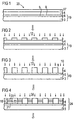
- an electrically conductive semiconductor layer 6 (for example a buffer layer) is applied to a main surface 5 of a growth substrate wafer 3 preferably made of SiC, for example by means of MOVPE (metal organic vapor phase epitaxy).
- B. consists of GaN and / or AlGaN.
- a mask layer 4, for example consisting of SiO 2 or Si x N 1-x is subsequently applied to this substrate wafer 19 consisting of the growth substrate 3 and the semiconductor layer 6, on which in turn a photoresist layer 17 is deposited.
- the wafer 20 produced in this way is shown schematically in FIG. 1.
- the photoresist layer 17 becomes the mask layer 4, for example in a manner known per se by means of a isotropic wet chemical (e.g. photo-etching solution) or by means of a dry chemical etching process 12 ( Figure 2), the is preferably selective for the material of the semiconductor layer 6, with a plurality of mask openings 10 (windows) provided such that in the mask openings 10 from the Growth substrate 3 facing away from the main surface 9 of the Semiconductor layer 6 is exposed ( Figure 3).
- a isotropic wet chemical e.g. photo-etching solution
- a dry chemical etching process 12 Figure 2
- a Ga (In, Al) N semiconductor layer sequence 18 (FIG. 4), consisting of a plurality of, is applied, for example, by means of organometallic vapor phase epitaxy (MOVPE) 13 (FIG. 3) onto the main surface 9 of the semiconductor layer 6 exposed in the windows 10 Ga (In, Al) N layers selectively epitaxially deposited.
- MOVPE organometallic vapor phase epitaxy
- semiconductor material of the light-emitting diode structure is deposited epitaxially, ie monocrystalline, only on the main surface 9 of the semiconductor layer 6 and not on the mask layer 4. Only a polycrystalline growth takes place on the mask layer 4, if at all.
- the Ga (In, Al) N semiconductor layer sequence 18 has, for example, a light-emitting active layer 23 arranged between an n-doped 21 and a p-doped Ga y Al 1-y N (0 ⁇ y ⁇ 1) cladding layer 22 consists of n-doped In x Ga 1-x N (0 ⁇ x ⁇ 1).
- compositions, layer thicknesses, doping etc. of the individual layers of Ga (In, Al) N semiconductor layer sequences 18 for light-emitting diode chips 100 are known in semiconductor technology and are therefore not explained in more detail here. The same applies to the etching processes for the isotropic and anisotropic etching of Sio 2 and Si x N 1-x .
- the one facing away from the light emitting diode structures 2 Side of the substrate wafer 3 before or after processing the Light-emitting diode structures 2 with a rear-side contact metallization layer 16 provided.
- the mask layer 4 Semiconductor layer 6 applied to the growth substrate 3 become. Rather, the mask layer 4 can directly on the Main surface 5 of the growth substrate 3, which then alone Forms substrate wafer 19 to be deposited.
- the selective Epitaxy of the light emitting diode structures 2 if necessary including the buffer layer is then made after the Window 10 in the mask layer 4 also on the Main surface 5 of the growth substrate 3.
- VCSEL Very Cavity Surface Emitting laser
- a mask layer 4 is applied over the entire surface of a main surface 9 of a substrate wafer 19, on which a semiconductor layer 6 can already be applied (indicated by dashed lines in the figures).
- the growth substrate 3 consists for example of SiC or sapphire and the mask layer 4 of SiO 2 or Si x N 1-x .
- the semiconductor layer 6 is, for example, an Al x Ga 1-x N epitaxial layer (0 x x 1 1) and serves z. B. as a buffer layer.
- a plurality of windows 10 (for example a round, rectangular or square recess or trench) in which the main surface 9 of the substrate wafer 19 is exposed are subsequently formed, for example by means of wet or dry etching, in the mask layer 4.
- Etching agents for etching SiO 2 or Si x N 1-x are known in semiconductor technology and are therefore not explained in more detail here.
- the exposed main area 9 of the substrate wafer 19 by means of selective epitaxy Semiconductor layer sequence 2 of an edge emitting Laser structure based on Ga (In, Al) N applied.
- the Windows 10 each have two opposite one another plane-parallel surface areas 7, the two laser mirror surfaces 8 lying plane-parallel to one another Define edge emitting laser structures 2.
- Selective epitaxy means that the semiconductor material of the Semiconductor layer sequence only on the substrate surface and not epitaxially on the mask layer, i.e. single crystal is deposited.
- the window 10 is closed by means of a first Substrate wafer 19 selective etching step and the Mask layer 4 is covered by means of a second Semiconductor layer sequence 2 selective etching step removed.
- the mask layer 4 is, for example, by means of wet or dry chemical etching of the substrate wafer 19 removed, so that the semiconductor layer sequence 2 as a laser semiconductor body remains free-standing on the substrate 3.
- the wafer produced in this way then becomes edge-emitting Laser chips 200 isolated.
Landscapes
- Physics & Mathematics (AREA)
- Condensed Matter Physics & Semiconductors (AREA)
- General Physics & Mathematics (AREA)
- Electromagnetism (AREA)
- Optics & Photonics (AREA)
- Led Devices (AREA)
- Semiconductor Lasers (AREA)
- Drying Of Semiconductors (AREA)
- Weting (AREA)
- Physical Vapour Deposition (AREA)
Applications Claiming Priority (4)
| Application Number | Priority Date | Filing Date | Title |
|---|---|---|---|
| DE19741442A DE19741442A1 (de) | 1997-09-19 | 1997-09-19 | Verfahren zum Herstellen einer Halbleitervorrichtung |
| DE19741442 | 1997-09-19 | ||
| DE19838810A DE19838810B4 (de) | 1998-08-26 | 1998-08-26 | Verfahren zum Herstellen einer Mehrzahl von Ga(In,Al)N-Leuchtdiodenchips |
| DE19838810 | 1998-08-26 |
Publications (3)
| Publication Number | Publication Date |
|---|---|
| EP0903792A2 true EP0903792A2 (fr) | 1999-03-24 |
| EP0903792A3 EP0903792A3 (fr) | 2000-03-22 |
| EP0903792B1 EP0903792B1 (fr) | 2010-11-03 |
Family
ID=26040146
Family Applications (1)
| Application Number | Title | Priority Date | Filing Date |
|---|---|---|---|
| EP98117796A Expired - Lifetime EP0903792B1 (fr) | 1997-09-19 | 1998-09-18 | Procédé pour la réalisation d'une pluralité de lasers semi-conducteurs |
Country Status (6)
| Country | Link |
|---|---|
| US (1) | US6100104A (fr) |
| EP (1) | EP0903792B1 (fr) |
| JP (1) | JPH11154648A (fr) |
| CN (1) | CN1218997A (fr) |
| DE (1) | DE59814474D1 (fr) |
| TW (1) | TW393785B (fr) |
Cited By (2)
| Publication number | Priority date | Publication date | Assignee | Title |
|---|---|---|---|---|
| WO2000013239A1 (fr) * | 1998-08-26 | 2000-03-09 | Osram Opto Semiconductors Gmbh & Co. Ohg | PROCEDE POUR PRODUIRE UNE PLURALITE DE PUCES A DIODES LUMINESCENTES A BASE DE Ga(In,Al)N |
| EP2339650A1 (fr) * | 2000-07-18 | 2011-06-29 | Sony Corporation | Procédé de production pour des dispositfs luminescents |
Families Citing this family (63)
| Publication number | Priority date | Publication date | Assignee | Title |
|---|---|---|---|---|
| FR2769924B1 (fr) | 1997-10-20 | 2000-03-10 | Centre Nat Rech Scient | Procede de realisation d'une couche epitaxiale de nitrure de gallium, couche epitaxiale de nitrure de gallium et composant optoelectronique muni d'une telle couche |
| US6608327B1 (en) | 1998-02-27 | 2003-08-19 | North Carolina State University | Gallium nitride semiconductor structure including laterally offset patterned layers |
| US6051849A (en) | 1998-02-27 | 2000-04-18 | North Carolina State University | Gallium nitride semiconductor structures including a lateral gallium nitride layer that extends from an underlying gallium nitride layer |
| US6265289B1 (en) | 1998-06-10 | 2001-07-24 | North Carolina State University | Methods of fabricating gallium nitride semiconductor layers by lateral growth from sidewalls into trenches, and gallium nitride semiconductor structures fabricated thereby |
| US6177688B1 (en) | 1998-11-24 | 2001-01-23 | North Carolina State University | Pendeoepitaxial gallium nitride semiconductor layers on silcon carbide substrates |
| US6255198B1 (en) * | 1998-11-24 | 2001-07-03 | North Carolina State University | Methods of fabricating gallium nitride microelectronic layers on silicon layers and gallium nitride microelectronic structures formed thereby |
| US20010042866A1 (en) * | 1999-02-05 | 2001-11-22 | Carrie Carter Coman | Inxalygazn optical emitters fabricated via substrate removal |
| US7004644B1 (en) * | 1999-06-29 | 2006-02-28 | Finisar Corporation | Hermetic chip-scale package for photonic devices |
| US6265322B1 (en) * | 1999-09-21 | 2001-07-24 | Agere Systems Guardian Corp. | Selective growth process for group III-nitride-based semiconductors |
| US6521514B1 (en) | 1999-11-17 | 2003-02-18 | North Carolina State University | Pendeoepitaxial methods of fabricating gallium nitride semiconductor layers on sapphire substrates |
| US6380108B1 (en) | 1999-12-21 | 2002-04-30 | North Carolina State University | Pendeoepitaxial methods of fabricating gallium nitride semiconductor layers on weak posts, and gallium nitride semiconductor structures fabricated thereby |
| US6403451B1 (en) | 2000-02-09 | 2002-06-11 | Noerh Carolina State University | Methods of fabricating gallium nitride semiconductor layers on substrates including non-gallium nitride posts |
| US6261929B1 (en) * | 2000-02-24 | 2001-07-17 | North Carolina State University | Methods of forming a plurality of semiconductor layers using spaced trench arrays |
| JP2001303020A (ja) * | 2000-04-24 | 2001-10-31 | Sunstar Inc | 透明液状組成物 |
| DE10051465A1 (de) | 2000-10-17 | 2002-05-02 | Osram Opto Semiconductors Gmbh | Verfahren zur Herstellung eines Halbleiterbauelements auf GaN-Basis |
| JP5523277B2 (ja) * | 2000-04-26 | 2014-06-18 | オスラム オプト セミコンダクターズ ゲゼルシャフト ミット ベシュレンクテル ハフツング | 発光半導体素子並びに発光性半導体素子の製造方法 |
| WO2001082384A1 (fr) | 2000-04-26 | 2001-11-01 | Osram Opto Semiconductors Gmbh | Composant semi-conducteur emetteur de rayonnement et son procede de fabrication |
| JP2003533030A (ja) * | 2000-04-26 | 2003-11-05 | オスラム オプト セミコンダクターズ ゲゼルシャフト ミット ベシュレンクテル ハフツング | GaNをベースとする発光ダイオードチップおよび発光ダイオード構造素子の製造法 |
| TWI289944B (en) | 2000-05-26 | 2007-11-11 | Osram Opto Semiconductors Gmbh | Light-emitting-diode-element with a light-emitting-diode-chip |
| US6867539B1 (en) * | 2000-07-12 | 2005-03-15 | 3M Innovative Properties Company | Encapsulated organic electronic devices and method for making same |
| US6334971B1 (en) * | 2000-07-20 | 2002-01-01 | Wen-Ping Huang | Manufacturing method for diode group processed by injection molding on the surface |
| US6518079B2 (en) * | 2000-12-20 | 2003-02-11 | Lumileds Lighting, U.S., Llc | Separation method for gallium nitride devices on lattice-mismatched substrates |
| JP2002261327A (ja) | 2001-03-06 | 2002-09-13 | Sony Corp | 半導体発光素子及び半導体発光素子の製造方法 |
| US6610554B2 (en) * | 2001-04-18 | 2003-08-26 | Hyung Se Kim | Method of fabricating organic electroluminescent display |
| US20040029365A1 (en) * | 2001-05-07 | 2004-02-12 | Linthicum Kevin J. | Methods of fabricating gallium nitride microelectronic layers on silicon layers and gallium nitride microelectronic structures formed thereby |
| US20030189215A1 (en) | 2002-04-09 | 2003-10-09 | Jong-Lam Lee | Method of fabricating vertical structure leds |
| US8294172B2 (en) | 2002-04-09 | 2012-10-23 | Lg Electronics Inc. | Method of fabricating vertical devices using a metal support film |
| US6841802B2 (en) | 2002-06-26 | 2005-01-11 | Oriol, Inc. | Thin film light emitting diode |
| US6750071B2 (en) * | 2002-07-06 | 2004-06-15 | Optical Communication Products, Inc. | Method of self-aligning an oxide aperture with an annular intra-cavity contact in a long wavelength VCSEL |
| KR100495215B1 (ko) * | 2002-12-27 | 2005-06-14 | 삼성전기주식회사 | 수직구조 갈륨나이트라이드 발광다이오드 및 그 제조방법 |
| KR100483049B1 (ko) * | 2003-06-03 | 2005-04-15 | 삼성전기주식회사 | 수직구조 질화갈륨계 발광다이오드의 제조방법 |
| DE10335081A1 (de) * | 2003-07-31 | 2005-03-03 | Osram Opto Semiconductors Gmbh | Verfahren zur Herstellung einer Vielzahl von optoelektronischen Halbleiterchips und optoeleketronischer Halbleiterchip |
| DE10335080A1 (de) * | 2003-07-31 | 2005-03-03 | Osram Opto Semiconductors Gmbh | Verfahren zur Herstellung einer Vielzahl von optoelektronischen Halbleiterchips und optoelektronischer Halbleiterchip |
| JP4049723B2 (ja) * | 2003-09-04 | 2008-02-20 | 沖電気工業株式会社 | 窒化物半導体素子の製造方法及び窒化物半導体素子の製造装置 |
| US7355284B2 (en) * | 2004-03-29 | 2008-04-08 | Cree, Inc. | Semiconductor light emitting devices including flexible film having therein an optical element |
| US8513686B2 (en) * | 2004-09-22 | 2013-08-20 | Cree, Inc. | High output small area group III nitride LEDs |
| US8174037B2 (en) | 2004-09-22 | 2012-05-08 | Cree, Inc. | High efficiency group III nitride LED with lenticular surface |
| US7737459B2 (en) * | 2004-09-22 | 2010-06-15 | Cree, Inc. | High output group III nitride light emitting diodes |
| US7259402B2 (en) * | 2004-09-22 | 2007-08-21 | Cree, Inc. | High efficiency group III nitride-silicon carbide light emitting diode |
| US8288942B2 (en) | 2004-12-28 | 2012-10-16 | Cree, Inc. | High efficacy white LED |
| US8901699B2 (en) | 2005-05-11 | 2014-12-02 | Cree, Inc. | Silicon carbide junction barrier Schottky diodes with suppressed minority carrier injection |
| JP2006339418A (ja) * | 2005-06-02 | 2006-12-14 | Seiko Epson Corp | 光素子及びその製造方法 |
| US8168000B2 (en) | 2005-06-15 | 2012-05-01 | International Rectifier Corporation | III-nitride semiconductor device fabrication |
| US20070049048A1 (en) * | 2005-08-31 | 2007-03-01 | Shahid Rauf | Method and apparatus for improving nitrogen profile during plasma nitridation |
| EP1925039A4 (fr) * | 2005-09-16 | 2012-07-04 | Showa Denko Kk | Procede de fabrication d'un dispositif lumineux a semi-conducteur nitrure |
| WO2007142946A2 (fr) | 2006-05-31 | 2007-12-13 | Cree Led Lighting Solutions, Inc. | Dispositif et procédé d'éclairage |
| JP4997502B2 (ja) * | 2006-09-20 | 2012-08-08 | 国立大学法人東北大学 | 半導体素子の製造方法 |
| US20080187018A1 (en) * | 2006-10-19 | 2008-08-07 | Amberwave Systems Corporation | Distributed feedback lasers formed via aspect ratio trapping |
| JP2009032971A (ja) * | 2007-07-27 | 2009-02-12 | Rohm Co Ltd | 窒化物半導体素子の製造方法 |
| CN101465319B (zh) * | 2007-12-17 | 2010-11-03 | 洲磊曜富科技股份有限公司 | 形成发光二极管元件的方法 |
| DE102009024311A1 (de) * | 2009-06-05 | 2011-01-05 | Fraunhofer-Gesellschaft zur Förderung der angewandten Forschung e.V. | Halbleiterbauelement und Verfahren zu seiner Herstellung |
| DE102009035429A1 (de) * | 2009-07-31 | 2011-02-03 | Osram Opto Semiconductors Gmbh | Leuchtdiodenchip |
| DE102010012423A1 (de) * | 2009-12-21 | 2011-06-22 | OSRAM Opto Semiconductors GmbH, 93055 | Lumineszenzdiodenanordnung, Hinterleuchtungsvorrichtung und Anzeigevorrichtung |
| CN101950783A (zh) * | 2010-08-23 | 2011-01-19 | 厦门市三安光电科技有限公司 | 氮化镓基高亮度发光二极管芯片的制作工艺 |
| CN102456788B (zh) * | 2010-10-20 | 2014-08-27 | 展晶科技(深圳)有限公司 | 发光二极管及其制造方法 |
| CN102456778B (zh) * | 2010-10-26 | 2014-11-05 | 展晶科技(深圳)有限公司 | 发光二极管芯片制造方法 |
| CN102130230A (zh) * | 2010-12-28 | 2011-07-20 | 中国科学院半导体研究所 | 发光二极管的制备方法 |
| CN105720136B (zh) * | 2014-12-02 | 2019-04-05 | 无锡极目科技有限公司 | 在复合玻璃基板上制造视频显示板用多色led的方法 |
| US10186833B2 (en) * | 2015-02-18 | 2019-01-22 | Ii-Vi Incorporated | Densely-spaced laser diode configurations |
| TW201933625A (zh) | 2018-01-19 | 2019-08-16 | 晶元光電股份有限公司 | 發光元件及其製造方法 |
| CN111326948B (zh) * | 2018-12-15 | 2023-04-07 | 深圳市中光工业技术研究院 | 激光器芯片的制备方法 |
| CN110690106A (zh) * | 2019-10-22 | 2020-01-14 | 北京大学东莞光电研究院 | 一种单晶金刚石芯片的制备方法 |
| CN114373835A (zh) * | 2021-12-24 | 2022-04-19 | 季华实验室 | 微显示芯片阵列的制作方法 |
Family Cites Families (11)
| Publication number | Priority date | Publication date | Assignee | Title |
|---|---|---|---|---|
| US5013682A (en) * | 1986-10-22 | 1991-05-07 | Texas Instruments Incorporated | Method for selective epitaxy using a WSI mask |
| JPH02260416A (ja) * | 1989-03-31 | 1990-10-23 | Toshiba Corp | 半導体装置の製造方法 |
| JP2943510B2 (ja) * | 1991-08-09 | 1999-08-30 | 日本電気株式会社 | 可変波長半導体レーザ装置 |
| JPH05251738A (ja) * | 1992-03-05 | 1993-09-28 | Fujitsu Ltd | 半導体光素子アレイの作製方法 |
| US5578839A (en) * | 1992-11-20 | 1996-11-26 | Nichia Chemical Industries, Ltd. | Light-emitting gallium nitride-based compound semiconductor device |
| DE69324445T2 (de) * | 1992-11-27 | 1999-09-30 | Denso Corp., Kariya | Tragbares elektronisches Gerät |
| JP2748354B2 (ja) * | 1993-10-21 | 1998-05-06 | 日亜化学工業株式会社 | 窒化ガリウム系化合物半導体チップの製造方法 |
| US5478774A (en) * | 1994-06-15 | 1995-12-26 | Motorola | Method of fabricating patterned-mirror VCSELs using selective growth |
| JP3246207B2 (ja) * | 1994-08-04 | 2002-01-15 | 松下電器産業株式会社 | 半導体レーザの製造方法 |
| JPH08316582A (ja) * | 1995-05-19 | 1996-11-29 | Nec Corp | 半導体レーザ |
| JPH0945987A (ja) * | 1995-07-31 | 1997-02-14 | Hitachi Ltd | 半導体レーザ素子 |
-
1998
- 1998-09-15 TW TW087115349A patent/TW393785B/zh not_active IP Right Cessation
- 1998-09-18 EP EP98117796A patent/EP0903792B1/fr not_active Expired - Lifetime
- 1998-09-18 DE DE59814474T patent/DE59814474D1/de not_active Expired - Lifetime
- 1998-09-19 CN CN98124519.6A patent/CN1218997A/zh active Pending
- 1998-09-21 JP JP26681998A patent/JPH11154648A/ja active Pending
- 1998-09-21 US US09/157,649 patent/US6100104A/en not_active Expired - Lifetime
Cited By (4)
| Publication number | Priority date | Publication date | Assignee | Title |
|---|---|---|---|---|
| WO2000013239A1 (fr) * | 1998-08-26 | 2000-03-09 | Osram Opto Semiconductors Gmbh & Co. Ohg | PROCEDE POUR PRODUIRE UNE PLURALITE DE PUCES A DIODES LUMINESCENTES A BASE DE Ga(In,Al)N |
| EP2339650A1 (fr) * | 2000-07-18 | 2011-06-29 | Sony Corporation | Procédé de production pour des dispositfs luminescents |
| EP2341530A1 (fr) * | 2000-07-18 | 2011-07-06 | Sony Corporation | Procédé de production d'un ensemble des dispositfs semiconducteurs |
| US8409886B2 (en) | 2000-07-18 | 2013-04-02 | Sony Corporation | Method of producing image display unit |
Also Published As
| Publication number | Publication date |
|---|---|
| EP0903792B1 (fr) | 2010-11-03 |
| DE59814474D1 (de) | 2010-12-16 |
| EP0903792A3 (fr) | 2000-03-22 |
| US6100104A (en) | 2000-08-08 |
| TW393785B (en) | 2000-06-11 |
| CN1218997A (zh) | 1999-06-09 |
| JPH11154648A (ja) | 1999-06-08 |
Similar Documents
| Publication | Publication Date | Title |
|---|---|---|
| EP0903792B1 (fr) | Procédé pour la réalisation d'une pluralité de lasers semi-conducteurs | |
| DE69918643T2 (de) | GaN Film mit reduzierter Verspannungsdichte und Herstellungsverfahren | |
| DE69503193T2 (de) | Dioden-Halbleiterlaser auf Basis von Nitridverbindungen der Gruppe III | |
| EP2270875B1 (fr) | Dispositf à semiconducteur émetteur de lumière et son procédé de fabrication | |
| DE69204828T2 (de) | Herstellung von Laserdioden mit durch Spaltung erzeugten Stirnflächen auf einem vollständigen Wafer. | |
| DE60017637T2 (de) | Verfahren zum Trennen einer epitaktischen Schicht von einem Substrat und ihre Übertragung auf ein anderes Substrat | |
| EP1920469B1 (fr) | Procede pour separer lateralement une plaquette a semi-conducteurs et element optoelectronique | |
| DE112004002809B9 (de) | Verfahren zum Herstellen eines strahlungsemittierenden Halbleiterchips und durch dieses Verfahren hergestellter Halbleiterchip | |
| EP2248235B1 (fr) | Laser à semi-conducteurs à émission par la tranche et procédé de fabrication d'un laser à semi-conducteurs à émission par la tranche | |
| EP1920508B1 (fr) | Procédé pour séparer latéralement une plaquette de semi-conducteurs empilés | |
| DE102014223196A1 (de) | Verfahren zur Herstellung von Gallium und Stickstoff tragenden Laser-Bauelementen mit verbesserter Verwendung von Substratmaterial | |
| DE10042947A1 (de) | Strahlungsemittierendes Halbleiterbauelement auf GaN-Basis | |
| EP2112699A2 (fr) | Produit semi-conducteur nitrure et son procédé de fabrication | |
| DE10312214A1 (de) | Verfahren zum Herstellen von mindestens einer Mesa- oder Stegstruktur oder von mindestens einem elektrisch gepumpten Bereich in einer Schicht oder Schichtenfolge | |
| DE19838810B4 (de) | Verfahren zum Herstellen einer Mehrzahl von Ga(In,Al)N-Leuchtdiodenchips | |
| WO2022090446A1 (fr) | Procédé de production de corps semi-conducteur et dispositif à semi-conducteur | |
| DE69925547T2 (de) | Herstellung der Endflächen von Laserdioden durch Epitaxie auf Basis von III-V Materialien | |
| DE112022002708T5 (de) | Verfahren zur herstellung eines halbleiterbauelements und halbleiterbauelement | |
| DE10327612B4 (de) | Verfahren zur Herstellung einer Mehrzahl von Halbleiterchips | |
| DE10252060B4 (de) | Strahlungsemittierendes Halbleiterbauelement und Verfahren zur Herstellung einer Vielzahl von Halbleiterschichten | |
| DE112020003346B4 (de) | Kantenemittierende halbleiterlaserdiode und verfahren zur herstellung einer solchen | |
| DE19741442A1 (de) | Verfahren zum Herstellen einer Halbleitervorrichtung | |
| DE102014223196B4 (de) | Verfahren zur Herstellung von Gallium und Stickstoff tragenden Laser-Bauelementen mit verbesserter Verwendung von Substratmaterial | |
| DE102008010511A1 (de) | Optoelektronischer Halbleiterkörper und Verfahren zu dessen Herstellung | |
| EP1649497B1 (fr) | Procede de fabrication d'une pluralite de puces a semi-conducteur optoelectroniques et puce a semi-conducteur optoelectronique ainsi obtenue |
Legal Events
| Date | Code | Title | Description |
|---|---|---|---|
| PUAI | Public reference made under article 153(3) epc to a published international application that has entered the european phase |
Free format text: ORIGINAL CODE: 0009012 |
|
| AK | Designated contracting states |
Kind code of ref document: A2 Designated state(s): DE FR GB IT |
|
| AX | Request for extension of the european patent |
Free format text: AL;LT;LV;MK;RO;SI |
|
| PUAL | Search report despatched |
Free format text: ORIGINAL CODE: 0009013 |
|
| AK | Designated contracting states |
Kind code of ref document: A3 Designated state(s): AT BE CH CY DE DK ES FI FR GB GR IE IT LI LU MC NL PT SE |
|
| AX | Request for extension of the european patent |
Free format text: AL;LT;LV;MK;RO;SI |
|
| RIC1 | Information provided on ipc code assigned before grant |
Free format text: 7H 01L 33/00 A, 7H 01S 3/085 B, 7H 01S 3/25 B |
|
| RAP1 | Party data changed (applicant data changed or rights of an application transferred) |
Owner name: OSRAM OPTO SEMICONDUCTORS GMBH & CO. OHG |
|
| 17P | Request for examination filed |
Effective date: 20000616 |
|
| 17Q | First examination report despatched |
Effective date: 20000913 |
|
| AKX | Designation fees paid |
Free format text: DE FR GB IT |
|
| RAP1 | Party data changed (applicant data changed or rights of an application transferred) |
Owner name: OSRAM OPTO SEMICONDUCTORS GMBH |
|
| RIC1 | Information provided on ipc code assigned before grant |
Ipc: H01L 33/00 20100101ALI20100324BHEP Ipc: H01S 5/02 20060101AFI20100324BHEP |
|
| RTI1 | Title (correction) |
Free format text: METHOD OF MANUFACTURING A PLURALITY OF SEMICONDUCTOR LASERS |
|
| GRAP | Despatch of communication of intention to grant a patent |
Free format text: ORIGINAL CODE: EPIDOSNIGR1 |
|
| GRAS | Grant fee paid |
Free format text: ORIGINAL CODE: EPIDOSNIGR3 |
|
| GRAA | (expected) grant |
Free format text: ORIGINAL CODE: 0009210 |
|
| AK | Designated contracting states |
Kind code of ref document: B1 Designated state(s): DE FR GB IT |
|
| REG | Reference to a national code |
Ref country code: GB Ref legal event code: FG4D Free format text: NOT ENGLISH |
|
| REF | Corresponds to: |
Ref document number: 59814474 Country of ref document: DE Date of ref document: 20101216 Kind code of ref document: P |
|
| PLBE | No opposition filed within time limit |
Free format text: ORIGINAL CODE: 0009261 |
|
| STAA | Information on the status of an ep patent application or granted ep patent |
Free format text: STATUS: NO OPPOSITION FILED WITHIN TIME LIMIT |
|
| 26N | No opposition filed |
Effective date: 20110804 |
|
| REG | Reference to a national code |
Ref country code: DE Ref legal event code: R097 Ref document number: 59814474 Country of ref document: DE Effective date: 20110804 |
|
| PG25 | Lapsed in a contracting state [announced via postgrant information from national office to epo] |
Ref country code: IT Free format text: LAPSE BECAUSE OF FAILURE TO SUBMIT A TRANSLATION OF THE DESCRIPTION OR TO PAY THE FEE WITHIN THE PRESCRIBED TIME-LIMIT Effective date: 20101103 |
|
| REG | Reference to a national code |
Ref country code: FR Ref legal event code: PLFP Year of fee payment: 18 |
|
| PGFP | Annual fee paid to national office [announced via postgrant information from national office to epo] |
Ref country code: GB Payment date: 20150917 Year of fee payment: 18 Ref country code: DE Payment date: 20150922 Year of fee payment: 18 |
|
| PGFP | Annual fee paid to national office [announced via postgrant information from national office to epo] |
Ref country code: FR Payment date: 20150922 Year of fee payment: 18 |
|
| REG | Reference to a national code |
Ref country code: DE Ref legal event code: R119 Ref document number: 59814474 Country of ref document: DE |
|
| GBPC | Gb: european patent ceased through non-payment of renewal fee |
Effective date: 20160918 |
|
| REG | Reference to a national code |
Ref country code: FR Ref legal event code: ST Effective date: 20170531 |
|
| PG25 | Lapsed in a contracting state [announced via postgrant information from national office to epo] |
Ref country code: DE Free format text: LAPSE BECAUSE OF NON-PAYMENT OF DUE FEES Effective date: 20170401 Ref country code: GB Free format text: LAPSE BECAUSE OF NON-PAYMENT OF DUE FEES Effective date: 20160918 Ref country code: FR Free format text: LAPSE BECAUSE OF NON-PAYMENT OF DUE FEES Effective date: 20160930 |