EP0899712B1 - Spaltentreiber für eine Flussigkristall-Anzeigeeinrichtung mit Aktiver Matrix - Google Patents
Spaltentreiber für eine Flussigkristall-Anzeigeeinrichtung mit Aktiver Matrix Download PDFInfo
- Publication number
- EP0899712B1 EP0899712B1 EP98402138A EP98402138A EP0899712B1 EP 0899712 B1 EP0899712 B1 EP 0899712B1 EP 98402138 A EP98402138 A EP 98402138A EP 98402138 A EP98402138 A EP 98402138A EP 0899712 B1 EP0899712 B1 EP 0899712B1
- Authority
- EP
- European Patent Office
- Prior art keywords
- source follower
- liquid crystal
- converter
- crystal display
- transistor
- Prior art date
- Legal status (The legal status is an assumption and is not a legal conclusion. Google has not performed a legal analysis and makes no representation as to the accuracy of the status listed.)
- Expired - Lifetime
Links
Images


Classifications
-
- G—PHYSICS
- G09—EDUCATION; CRYPTOGRAPHY; DISPLAY; ADVERTISING; SEALS
- G09G—ARRANGEMENTS OR CIRCUITS FOR CONTROL OF INDICATING DEVICES USING STATIC MEANS TO PRESENT VARIABLE INFORMATION
- G09G3/00—Control arrangements or circuits, of interest only in connection with visual indicators other than cathode-ray tubes
- G09G3/20—Control arrangements or circuits, of interest only in connection with visual indicators other than cathode-ray tubes for presentation of an assembly of a number of characters, e.g. a page, by composing the assembly by combination of individual elements arranged in a matrix no fixed position being assigned to or needed to be assigned to the individual characters or partial characters
- G09G3/2007—Display of intermediate tones
- G09G3/2011—Display of intermediate tones by amplitude modulation
-
- G—PHYSICS
- G09—EDUCATION; CRYPTOGRAPHY; DISPLAY; ADVERTISING; SEALS
- G09G—ARRANGEMENTS OR CIRCUITS FOR CONTROL OF INDICATING DEVICES USING STATIC MEANS TO PRESENT VARIABLE INFORMATION
- G09G3/00—Control arrangements or circuits, of interest only in connection with visual indicators other than cathode-ray tubes
- G09G3/20—Control arrangements or circuits, of interest only in connection with visual indicators other than cathode-ray tubes for presentation of an assembly of a number of characters, e.g. a page, by composing the assembly by combination of individual elements arranged in a matrix no fixed position being assigned to or needed to be assigned to the individual characters or partial characters
- G09G3/34—Control arrangements or circuits, of interest only in connection with visual indicators other than cathode-ray tubes for presentation of an assembly of a number of characters, e.g. a page, by composing the assembly by combination of individual elements arranged in a matrix no fixed position being assigned to or needed to be assigned to the individual characters or partial characters by control of light from an independent source
- G09G3/36—Control arrangements or circuits, of interest only in connection with visual indicators other than cathode-ray tubes for presentation of an assembly of a number of characters, e.g. a page, by composing the assembly by combination of individual elements arranged in a matrix no fixed position being assigned to or needed to be assigned to the individual characters or partial characters by control of light from an independent source using liquid crystals
- G09G3/3611—Control of matrices with row and column drivers
- G09G3/3685—Details of drivers for data electrodes
-
- G—PHYSICS
- G09—EDUCATION; CRYPTOGRAPHY; DISPLAY; ADVERTISING; SEALS
- G09G—ARRANGEMENTS OR CIRCUITS FOR CONTROL OF INDICATING DEVICES USING STATIC MEANS TO PRESENT VARIABLE INFORMATION
- G09G2310/00—Command of the display device
- G09G2310/02—Addressing, scanning or driving the display screen or processing steps related thereto
- G09G2310/0243—Details of the generation of driving signals
- G09G2310/0248—Precharge or discharge of column electrodes before or after applying exact column voltages
-
- G—PHYSICS
- G09—EDUCATION; CRYPTOGRAPHY; DISPLAY; ADVERTISING; SEALS
- G09G—ARRANGEMENTS OR CIRCUITS FOR CONTROL OF INDICATING DEVICES USING STATIC MEANS TO PRESENT VARIABLE INFORMATION
- G09G2310/00—Command of the display device
- G09G2310/02—Addressing, scanning or driving the display screen or processing steps related thereto
- G09G2310/0264—Details of driving circuits
- G09G2310/027—Details of drivers for data electrodes, the drivers handling digital grey scale data, e.g. use of D/A converters
-
- G—PHYSICS
- G09—EDUCATION; CRYPTOGRAPHY; DISPLAY; ADVERTISING; SEALS
- G09G—ARRANGEMENTS OR CIRCUITS FOR CONTROL OF INDICATING DEVICES USING STATIC MEANS TO PRESENT VARIABLE INFORMATION
- G09G2310/00—Command of the display device
- G09G2310/02—Addressing, scanning or driving the display screen or processing steps related thereto
- G09G2310/0264—Details of driving circuits
- G09G2310/0291—Details of output amplifiers or buffers arranged for use in a driving circuit
-
- G—PHYSICS
- G09—EDUCATION; CRYPTOGRAPHY; DISPLAY; ADVERTISING; SEALS
- G09G—ARRANGEMENTS OR CIRCUITS FOR CONTROL OF INDICATING DEVICES USING STATIC MEANS TO PRESENT VARIABLE INFORMATION
- G09G2330/00—Aspects of power supply; Aspects of display protection and defect management
- G09G2330/02—Details of power systems and of start or stop of display operation
- G09G2330/021—Power management, e.g. power saving
-
- G—PHYSICS
- G09—EDUCATION; CRYPTOGRAPHY; DISPLAY; ADVERTISING; SEALS
- G09G—ARRANGEMENTS OR CIRCUITS FOR CONTROL OF INDICATING DEVICES USING STATIC MEANS TO PRESENT VARIABLE INFORMATION
- G09G3/00—Control arrangements or circuits, of interest only in connection with visual indicators other than cathode-ray tubes
- G09G3/20—Control arrangements or circuits, of interest only in connection with visual indicators other than cathode-ray tubes for presentation of an assembly of a number of characters, e.g. a page, by composing the assembly by combination of individual elements arranged in a matrix no fixed position being assigned to or needed to be assigned to the individual characters or partial characters
- G09G3/34—Control arrangements or circuits, of interest only in connection with visual indicators other than cathode-ray tubes for presentation of an assembly of a number of characters, e.g. a page, by composing the assembly by combination of individual elements arranged in a matrix no fixed position being assigned to or needed to be assigned to the individual characters or partial characters by control of light from an independent source
- G09G3/36—Control arrangements or circuits, of interest only in connection with visual indicators other than cathode-ray tubes for presentation of an assembly of a number of characters, e.g. a page, by composing the assembly by combination of individual elements arranged in a matrix no fixed position being assigned to or needed to be assigned to the individual characters or partial characters by control of light from an independent source using liquid crystals
- G09G3/3611—Control of matrices with row and column drivers
- G09G3/3685—Details of drivers for data electrodes
- G09G3/3688—Details of drivers for data electrodes suitable for active matrices only
Definitions
- the present invention relates to a liquid crystal display device, and more particularly to an output circuit relative to column lines of a column driver in an active matrix liquid crystal display device.
- Fig. 7 shows an exemplary structure of an active matrix liquid crystal display device.
- a liquid crystal panel 102 is composed of liquid crystal cells (pixels) 101 arrayed to form a two-dimensional matrix, and a vertical (row) driver 103 for row selection and a horizontal (column) driver (column line driving circuit) 104 for column selection are provided in the periphery of the liquid crystal panel 102.
- the horizontal driver 104 comprises a shift register 111 having a plurality of stages corresponding to the number n of column lines, a shift register controller 112 for controlling the shift register 111, a sampling circuit 113 for sampling data on a data bus line in synchronism with sampling pulses outputted successively from the shift register 111, a latch circuit 114 for holding the sampled data during one horizontal period, a DA converter 115 for converting the latch data into analog signal, and an output circuit 118 consisting of n output buffers 117-1 - 117-n for driving the column lines 116-1 - 116-n respectively.
- output ends of the output buffers 117-1 - 117-n are connected directly to the column lines 116-1 - 116-n, so that no problem is raised in particular if the output buffers 117-1 - 117-n structurally have sufficient driving capability with regard to both input and output currents.
- the output buffers 117-1 - 117-n are composed of source follower circuits for example and have sufficient driving capability merely in one direction.
- the output circuit needs to have a complete characteristic or a sufficient time for discharging the load.
- a power supply for the source follower circuit is required to furnish a current necessary for discharging the capacitive load, whereby the resultant power consumption is steadily rendered large.
- Document EP-A-0 510 696 relates to a liquid crystal display control system which comprises a liquid crystal panel, plural data latch means for storing digital data, and plural DA converters for converting the ouputs of the data latch means into analog signals to be applied to the liquid crystal panel.
- liquid crystal display system disclosed in this document does not comprise output buffers consisting of source follower circuits.
- Document EP-A-0 597 315 discloses a switched capacitor D/A converter in which a set of N digital bits serially supplied to an input node are converted to an analog voltage by means of N binary weighted capacitors and N switching transistors, one capacitor being associated with one switching for each one of the N digital data bits.
- a liquid crystal display device comprising output buffers corresponding to column lines, each of the output buffers consisting of a source follower circuit, analog switches provided between the source follower circuits and the column lines respectively, and a switch controller for on-off controlling the analog switches.
- a DA converter is provided in the preceding stage of the output buffers, and the switch controller turns off the analog switches during a DA conversion period of the DA converter or during a precharge period prior to DA conversion, and turns on the analog switches during a predetermined period other than such periods.
- the output buffers are disconnected from or connected to the column lines when the analog switches are turned off or turned on. Therefore, the output circuit can be separated from a capacitive load by disconnecting the output buffers from the column lines through turning off the analog switches during a DA conversion period of a DA converter provided in the preceding stage of the output circuit or during a precharge period prior to DA conversion, hence preventing increase of the output current of each output buffer while ensuring sufficient change of the signal potential.
- a liquid crystal display device having a horizontal driver and a vertical driver.
- the horizontal driver comprises a shift register having a plurality of stages equal in number to columns; a shift register controller for controlling the shift register; a sampling circuit for sampling data on a data bus line in synchronism with sampling pulses outputted successively from the shift register; a latch circuit for holding the sampled data during one horizontal period; a DA converter for converting into analog signal the data held by the latch circuit; output buffers for driving column lines; and analog switches provided between the column lines and the output buffers.
- the analog switches are on-off controlled by a switch controller.
- Fig. 1 schematically shows the structure of a liquid crystal display device according to the present invention
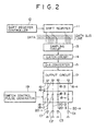
- Fig. 2 is a block diagram showing an embodiment of the present invention applied to a column driving circuit (horizontal driver) in a liquid crystal display device.
- Fig. 1 shows an exemplary structure of an active matrix liquid crystal display device.
- a liquid crystal panel 1020 is composed of liquid crystal cells (pixels) 1010 arrayed to form a two-dimensional matrix, and a vertical (row) driver 1030 for row selection and a horizontal (column) driver (column line driving circuit) 1040 for column selection are provided in the periphery of the liquid crystal panel 1020.
- the column driving circuit comprises a shift register 11 having a plurality of stages corresponding to the number n of column lines, a shift register controller 12 for controlling the shift register 11, a sampling circuit 13 for sampling data on a data bus line in synchronism with sampling pulses outputted successively from the shift register 11, a latch circuit 14 for holding and latching the sampled data during one horizontal period, a DA converter 15 for converting the latched data into analog signal, an output circuit 17 consisting of n output buffers 16-1 - 16-n for driving the column lines respectively, n analog switches 18-1 - 18-n, and a switch control pulse generator 19.
- Ends of the analog switches 18-1 - 18-n on one side thereof are connected to the output ends of the output buffers 16-1 - 16-n respectively, and the column lines 20-1 - 20-n are connected to the other ends of the analog switches 18-1 - 18-n. These column lines 20-1 - 20-n have capacitive loads Cl - Cn respectively.
- the switch control pulse generator 19 generates switch control pulses for on-off controlling the analog switches 18-1 - 18-n.
- the switch control pulse generator 19 turns off the analog switches 18-1 - 18-n during a DA conversion period of the DA converter 15 or during a precharge period prior to DA conversion to thereby disconnect the output buffers 16-1 - 16-n from the column lines 20-1 - 20-n respectively, and turns on the analog switches 18-1 - 18-n only during a predetermined period to thereby connect the output buffers 16-1 - 16-n to the column lines 20-1 - 20-n respectively.
- Fig. 3 shows an exemplary structure of the output buffers 16-1 - 16-n each consisting of a source follower circuit.
- one end of a first capacitor 23 is connected to a gate of an NMOS source follower transistor 21, and a first analog switch 25 is connected between the gate of the source follower transistor 21 and a precharge power supply 24.
- a second analog switch 26 is connected between the other end of the first capacitor 23 and the source of the source follower transistor 21, and a third analog switch 27 is connected between the other end of the first capacitor 23 and a signal source (Vin).
- An NMOS transistor 28 is cascode-connected to the drain of the source follower transistor 21, and a second capacitor 29 is connected between the gate of the source follower transistor 21 and the gate of the cascode transistor 28.
- a fourth analog switch 31 is connected between the gate of the cascode transistor 28 and a power supply 30 of a predetermined voltage Vc.
- the voltage Vc of the power supply 30 is set to a value shifted by a certain quantity from a precharge voltage Vpre of the source follower transistor 21. The shift quantity is calculated on the basis of saturation conditions of the source follower transistor 21 and the cascode transistor 28.
- the first and second analog switches 25 and 26 are turned on while the third analog switch 27 is turned off, whereby a predetermined precharge voltage Vpre is applied from the precharge power supply 24 to the gate of the source follower transistor 21 via the first analog switch 25.
- the first and second switches 25 and 26 are turned off while the third analog switch 27 is turned on, whereby the end of the first capacitor 23 which is connected to the source side of the source follower transistor 21 when the second switch 26 is turned on is connected again to the input signal Vin (signal source side) while the gate of the source follower transistor 21 is disconnected from the precharge power supply 24.
- the gate potential of the source follower transistor 21 is changed to Vin + Vos.
- the gate of the cascode transistor 28 is precharged to the voltage Vc by turning on the fourth analog switch 31 as well as the first and second analog switches 25 and 26. Subsequently in an output period, the gate of the cascode transistor 28 is disconnected from the power supply 30 by turning off the fourth analog switch 31.
- the gate potential of the cascode transistor 28 can be set higher than the supply voltage VCC due to such on-off action of the fourth analog switch 31, hence raising the drain voltage of the source follower transistor 21. Therefore, even if a polysilicon TFT or the like having a high threshold voltage Vth with large variation is used as the source follower transistor 21 to form a source follower circuit, the drain voltage range of the transistor 21 is widened to consequently achieve extension of the output dynamic range.
- precharging the first capacitor 23 can be performed by the precharge power supply 24 which is independent of the signal source, so that it is not necessary to diminish the output impedance of the signal source to an extremely small value. And the resultant merit attainable therefrom is remarkably great when the source follower circuit is used as an output circuit of a reference voltage selection type DA converter in the horizontal driver of a liquid crystal display device. That is, the width of its reference voltage line can be narrowed to eventually realize dimensional reduction of the whole circuit.
- the advantages attainable due to such circuit operation are effective particularly when the source follower circuit is composed of a polysilicon TFT.
- the reason is as follows. Since a polysilicon TFT has no substrate potential, there is no substrate bias effect. Accordingly, when the output voltage (source potential of the source follower transistor 21) is changed as a result of any change in the input voltage (input potential of the source follower transistor 21), the threshold voltage Vth remains unchanged so that offset cancellation is performed with high accuracy.
- the parasitic capacitance on one-end side of the first analog switch 25 i.e., base side of the source follower transistor 21
- the parasitic capacitance on one-end side of the first analog switch 25 is rendered small so that, when the base potential of the source follower transistor 21 is changed, the offset charge stored in the first capacitor 23 is not released with ease.
- Fig. 5 shows a concrete configuration where a source follower circuit having the above-described offset cancel structure is employed as an output circuit in a column driver.
- Fig. 5 there is shown a circuit configuration relative merely to one column line 20-k alone, and any circuit components corresponding to those in Fig. 3 are denoted by like reference numerals or symbols.
- the aforementioned DA converter 15 provided in the preceding stage of the output circuit 17 shown in Fig. 2 comprises a reference voltage selection type DA converter 41 for three high-order bits b0 - b2 and a switched capacitor array type DA converter 42 for three low-order bits b3 - b5.
- capacitors of the switched capacitor array type DA converter 42 serve also as the offset storage capacitor 23 of the source follower circuit in the foregoing configuration.
- the combined capacitance of four capacitors 43, 44, 45 and 46 which are provided correspondingly to three low-order bits b3 - b5 and each of which is connected at one end thereof to the gate of the source follower transistor 21, corresponds to the offset storage capacitor 23.
- the capacitance values of such four capacitors 43, 44, 45, 46 are set to a ratio of 4Co:2Co:Co:Co.
- analog switches 47 - 50 which are connected between the other ends of the capacitors 43 - 46 and the source of the source follower transistor 21, correspond to the second analog switch 26, and four analog switches 51 - 54, which are connected between the other ends of the capacitors 43 - 46 and a signal source, correspond to the third analog switch 26.
- the analog switches 25, 47 - 50 and so forth are on-off controlled by a precharge pulse controller 55.
- an analog switch 18-k provided between the output end of an output buffer 16-k and a column line 20-k is on-off controlled by a switch control pulse generated from a switch control pulse generator 19. More concretely, as shown in a signal timing chart of Fig. 6, the analog switch 18-k is turned off during a precharge period and a DA conversion period, but is turned on only during a predetermined period other than such periods.
- a source follower circuit having an offset cancel structure is employed as each of the output buffers 16-1 - 16-n in the column driver of the liquid crystal display device with the switched capacitor array type DA converter 14 for three low-order bits b3 - b5, whereby the offset storage capacitor 23 and the capacitors of the switched capacitor array type DA converter 42 can be used in common to consequently minimise the number of additionally required circuit elements, hence enhancing the efficiency.
- the output current of the source follower circuit shown in Fig. 5 can be obtained without any limit at a signal rise time, but is limited at a signal fall time to a maximum of the current Iref of a power supply 22. Therefore, if a large output load is connected at a signal fall time, it is impossible to change the signal sufficiently. For achieving sufficient change of the signal, a current Iref of a great value is required.
- the present invention is so contrived that, when the signal potential is widely decreased during a precharge period or the like, the analog switch 18-k is turned off during this period to disconnect the output buffer 16-k from the capacitive load Ck, whereby the output current of the source follower circuit is not increased to consequently enable sufficient change of the signal potential.
- a current Iref of merely a small value is enough in constituting a desired output circuit.
- the output period, during which the analog switch 18-k is turned on, may be set to a predetermined one other than the precharge period and the DA conversion period.
- k is a constant; and Cox, W and L denote the oxide film capacitance, the gate length and the gate width of the transistor, respectively.
- the offset potential Vgs is raised with increase of the current Iref.
- this brings about a result of narrowing the output dynamic range of the circuit.
- the transistor size needs to be enlarged for ensuring a desired dynamic range. If the current Iref is small in value, the transistor size can be diminished to consequently realize dimensional reduction of the circuit.
- the source follower circuit having the above-described offset cancel structure is rendered useful particularly when the column driving circuit (horizontal driver) is composed of a polysilicon TFT integrally with the liquid crystal panel.
- the column driving circuit horizontal driver
- the reason are as follows.
- analog switches are provided between output ends of the output buffers and the column lines, and the analog switches are on-off controlled in such a manner that the output buffers and the column lines are mutually disconnected in an off-state of the analog switches to thereby separate the output circuit from the capacitive load, hence avoiding increase of the output current of the output buffers. Therefore, it becomes possible to easily constitute an improved system which charges the column line loads by the unidirectional current buffers, with some advantages of realizing a lower power consumption, a dimensional reduction of the circuit, a wider dynamic range, and decrease of the output potential variation.
Claims (10)
- Flüssigkristallanzeigevorrichtung, die aufweist:Ausgangspuffer (16-1, ..., 16-n), die Spaltenleitungen (20-1, ..., 20-n) entsprechen, wobei jeder dieser Ausgangspuffer aus einer Sourcefolgerschaltung besteht,analoge Schalter (18-1, ..., 18-n), die zwischen den jeweiligen Sourcefolgerschaltungen und den Spaltenleitungen angeordnet sind, undeine Schaltersteuerung (19) zum Steuern des Ein- und Ausschaltens der analogen Schalter (18-1, ..., 18-n).
- Flüssigkristallanzeigevorrichtung nach Anspruch 1, bei der in der den Ausgangspuffern (16-1, ..., 16-n) vorangehenden Stufe ein D/A-Wandler (15) vorgesehen ist, und bei der die Schaltersteuerung (19) die analogen Schalter (18-1, ..., 18-n) während der D/A-Umwandlungsperiode des D/A-Wandlers (15) oder während einer Vorladeperiode vor der D/A-Umwandlung ausschaltet und die analogen Schalter (18-1, ..., 18-n) während einer vorbestimmten Periode, die von den genannten Perioden abweicht, einschaltet.
- Flüssigkristallanzeigevorrichtung nach Anspruch 1 oder 2, bei der jeder der genannten Ausgangspuffer (16-1, ..., 16-n) aus einer Sourcefolgerschaltung besteht, die aufweist:einen ersten Kondensator (23), der mit einem Ende mit dem Gate eines Sourcefolgertransistors (21) verbunden ist,einen ersten analogen Schalter (25), der zwischen dem Gate des Sourcefolgertransistors (21) und einer Vorlade-Stromversorgung angeordnet ist,einen zweiten analogen Schalter (26), der zwischen dem anderen Ende des ersten Kondensators (23) und der Source des Sourcefolgertransistors (21) angeordnet und mit dem ersten analogen Schalter gekoppelt ist,einen dritten analogen Schalter (27), der zwischen dem anderen Ende des ersten Kondensators (23) und einer Signalquelle (Vin) angeordnet ist und der invers zu der Ein-Aus-Betätigung des ersten und des zweiten analogen Schalters (25, 26) betätigt wird,einen Kaskodentransistor (28), der in Kaskodenschaltung mit der Drainseite des Sourcefolgertransistors (21) verbunden ist,einen zweiten Kondensator (29), der zwischen dem Gate des Sourcefolgertransistors (21) und dem Gate des Kaskodentransistors (28) angeordnet ist,und einen vierten analogen Schalter (31), der zwischen dem Gate des Kaskodentransistors (28) und einer vorbestimmten Stromversorgung (Vc) angeordnet ist und der mit dem ersten und dem zweiten analogen Schalter (25, 26) gekoppelt ist.
- Flüssigkristallanzeigevorrichtung nach Anspruch 3, bei der der D/A-Wandler (15) aus einem D/A-Wandler vom Referenzspannungsauswahltyp und einem D/A-Wandler vom geschalteten Kondensatorarraytyp besteht und bei der die Kondensatoren des D/A-Wandlers vom geschalteten Kondensatorarraytyp auch als die genannten ersten Kondensatoren (23) benutzt werden.
- Flüssigkristallanzeigevorrichtung nach Anspruch 3 oder 4, bei der die Sourcefolgerschaltung aus einem Polysilizium-Dünnfilm-Transistor besteht.
- Flüssigkristallanzeigevorrichtung nach Anspruch 1 mit einem Horizontaltreiber (1040) und einem Vertikaltreiber (1030), wobei der Horizontaltreiber (1040) aufweist:wobei das Ein- und Ausschalten der analogen Schalter (18-1, ..., 18-n) von einer Schaltersteuerung (19) gesteuert wird.ein Schieberegister (11) mit mehreren Stufen, deren Zahl gleich der Zahl der Spalten ist,eine Schieberegistersteuerung (12) zum Steuern des Schieberegisters (11),eine Abtastschaltung (13) zum Abtasten der Daten auf einer Datenbusleitung synchron mit Abtastimpulsen, die von dem Schieberegister (11) sukzessiv ausgegeben werden,eine Verriegelungsschaltung (14) zum Halten der abgetasteten Daten während einer horizontalen Periode,einen D/A-Wandler (15) zum Umwandeln der in der Verriegelungsschaltung (14) gehaltenen Daten in ein analoges SignalAusgangspuffer (16-1, ..., 16-n) für die Ansteuerung der Spaltenleitungen 20en (20-1, ..., 20-n) undanaloge Schalter (18-1, ..., 18-n), die zwischen den Spaltenleitungen (20-1, ..., 20-n) und den Ausgangspuffern (16-1, ..., 16-n) angeordnet sind,
- Flüssigkristallanzeigevorrichtung nach Anspruch 6, bei der die Schaltersteuerung (19) die analogen Schalter (18-1, ..., 18-n) während der D/A-Umwandlungsperiode des D/A-Wandlers (15) oder während einer Vorladeperiode vor der D/A-Umwandlung ausschaltet und die analogen Schalter (18-1, ..., 18-n) während einer vorbestimmten Periode, die von den genannten Perioden abweicht, einschaltet.
- Flüssigkristallanzeigevorrichtung nach Anspruch 6 oder 7, bei der jeder der genannten Ausgangspuffer (16-1, ..., 16-n) aus einer Sourcefolgerschaltung besteht, die aufweist:einen ersten Kondensator (23), der mit einem Ende mit dem Gate eines Sourcefolgertransistors (21) verbunden ist,einen ersten analogen Schalter (25), der zwischen dem Gate des Sourcefolgertransistors (21) und einer Vorlade-Stromversorgung angeordnet ist,einen zweiten analogen Schalter (26), der zwischen dem anderen Ende des ersten Kondensators (23) und der Source des Sourcefolgertransistors (21) angeordnet und mit dem ersten analogen Schalter gekoppelt ist,einen dritten analogen Schalter (27), der zwischen dem anderen Ende des ersten Kondensators (23) und einer Signalquelle (Vin) angeordnet ist und der invers zu der Ein-Aus-Betätigung des ersten und des zweiten analogen Schalters (25, 26) betätigt wird,einen Kaskodentransistor (28), der in Kaskodenschaltung mit der Drainseite des Sourcefolgertransistors (21) verbunden ist,einen zweiten Kondensator (29), der zwischen dem Gate des Sourcefolgertransistors (21) und dem Gate des Kaskodentransistors (28) angeordnet ist,und einen vierten analogen Schalter (31), der zwischen dem Gate des Kaskodentransistors (28) und einer vorbestimmten Stromversorgung (Vc) angeordnet ist und der mit dem ersten und dem zweiten analogen Schalter (25, 26) gekoppelt ist.
- Flüssigkristallanzeigevorrichtung nach Anspruch 8, bei der der D/A-Wandler (15) aus einem D/A-Wandler vom Referenzspannungsauswahltyp besteht und einem D/A-Wandler vom geschalteten Kondensatorarraytyp besteht und bei der die Kondensatoren des D/A-Wandlers vom geschalteten Kondensatorarraytyp auch als die genannten ersten Kondensatoren (23) benutzt werden.
- Flüssigkristallanzeigevorrichtung nach Anspruch 8 oder 9, bei der die Sourcefolgerschaltung aus einem Polysilizium-Dünnfilm-Transistor besteht.
Applications Claiming Priority (3)
| Application Number | Priority Date | Filing Date | Title |
|---|---|---|---|
| JP233517/97 | 1997-08-29 | ||
| JP23351797A JP4046811B2 (ja) | 1997-08-29 | 1997-08-29 | 液晶表示装置 |
| JP23351797 | 1997-08-29 |
Publications (3)
| Publication Number | Publication Date |
|---|---|
| EP0899712A2 EP0899712A2 (de) | 1999-03-03 |
| EP0899712A3 EP0899712A3 (de) | 2000-06-07 |
| EP0899712B1 true EP0899712B1 (de) | 2002-10-16 |
Family
ID=16956278
Family Applications (1)
| Application Number | Title | Priority Date | Filing Date |
|---|---|---|---|
| EP98402138A Expired - Lifetime EP0899712B1 (de) | 1997-08-29 | 1998-08-28 | Spaltentreiber für eine Flussigkristall-Anzeigeeinrichtung mit Aktiver Matrix |
Country Status (5)
| Country | Link |
|---|---|
| US (1) | US6181314B1 (de) |
| EP (1) | EP0899712B1 (de) |
| JP (1) | JP4046811B2 (de) |
| KR (1) | KR100564275B1 (de) |
| DE (1) | DE69808711T2 (de) |
Families Citing this family (52)
| Publication number | Priority date | Publication date | Assignee | Title |
|---|---|---|---|---|
| JP3613940B2 (ja) * | 1997-08-29 | 2005-01-26 | ソニー株式会社 | ソースフォロワ回路、液晶表示装置および液晶表示装置の出力回路 |
| KR100295679B1 (ko) * | 1999-03-30 | 2001-07-12 | 김영환 | 티에프티 엘씨디 칼럼 구동 장치 및 그 구동 방법 |
| KR100701892B1 (ko) * | 1999-05-21 | 2007-03-30 | 엘지.필립스 엘시디 주식회사 | 데이터라인 구동방법 및 그를 이용한 액정 표시장치 |
| KR100354204B1 (ko) * | 1999-10-21 | 2002-09-27 | 세이코 엡슨 가부시키가이샤 | 전압 공급 장치 및 그것을 사용한 반도체 장치, 전기 광학장치 및 전자 기기 |
| US6756962B1 (en) | 2000-02-10 | 2004-06-29 | Hitachi, Ltd. | Image display |
| TW522374B (en) * | 2000-08-08 | 2003-03-01 | Semiconductor Energy Lab | Electro-optical device and driving method of the same |
| JP4757388B2 (ja) * | 2001-01-15 | 2011-08-24 | 株式会社 日立ディスプレイズ | 画像表示装置およびその駆動方法 |
| JP2002311920A (ja) * | 2001-04-19 | 2002-10-25 | Matsushita Electric Ind Co Ltd | 液晶表示装置、画像表示応用機器、及び情報携帯端末機器 |
| TW526465B (en) * | 2001-04-27 | 2003-04-01 | Toshiba Corp | Display apparatus, digital/analog converting circuit and digital/analog converting method |
| US6594606B2 (en) * | 2001-05-09 | 2003-07-15 | Clare Micronix Integrated Systems, Inc. | Matrix element voltage sensing for precharge |
| US7079131B2 (en) * | 2001-05-09 | 2006-07-18 | Clare Micronix Integrated Systems, Inc. | Apparatus for periodic element voltage sensing to control precharge |
| US7079130B2 (en) * | 2001-05-09 | 2006-07-18 | Clare Micronix Integrated Systems, Inc. | Method for periodic element voltage sensing to control precharge |
| JP4269542B2 (ja) * | 2001-06-04 | 2009-05-27 | 日本電気株式会社 | トランジスタの動作点設定方法及びその回路、信号成分値変更方法並びにアクティブマトリクス型液晶表示装置 |
| US20030169241A1 (en) * | 2001-10-19 | 2003-09-11 | Lechevalier Robert E. | Method and system for ramp control of precharge voltage |
| WO2003033749A1 (en) * | 2001-10-19 | 2003-04-24 | Clare Micronix Integrated Syst | Matrix element precharge voltage adjusting apparatus and method |
| WO2003034390A2 (en) * | 2001-10-19 | 2003-04-24 | Clare Micronix Integrated Systems, Inc. | Precharge circuit and method for passive matrix oled display |
| TWI277290B (en) * | 2002-01-17 | 2007-03-21 | Semiconductor Energy Lab | Electric circuit |
| CN101257284B (zh) * | 2002-01-17 | 2011-10-19 | 株式会社半导体能源研究所 | 半导体器件 |
| JP2003283271A (ja) * | 2002-01-17 | 2003-10-03 | Semiconductor Energy Lab Co Ltd | 電気回路 |
| EP1331628A3 (de) * | 2002-01-22 | 2005-01-19 | Seiko Epson Corporation | Verfahren und Schaltkreis zur Ansteuerung eines Pixel |
| JP4252855B2 (ja) * | 2002-11-06 | 2009-04-08 | アルプス電気株式会社 | ソースフォロア回路および液晶表示装置の駆動装置 |
| DE10252166A1 (de) | 2002-11-09 | 2004-05-19 | Philips Intellectual Property & Standards Gmbh | Anzeigevorrichtung mit Pixelinversion |
| KR100898787B1 (ko) * | 2002-11-11 | 2009-05-20 | 엘지디스플레이 주식회사 | 액정표시장치 및 그 구동방법 |
| US6958651B2 (en) | 2002-12-03 | 2005-10-25 | Semiconductor Energy Laboratory Co., Ltd. | Analog circuit and display device using the same |
| WO2004061812A1 (ja) * | 2002-12-27 | 2004-07-22 | Semiconductor Energy Laboratory Co., Ltd. | 半導体装置およびそれを用いた表示装置 |
| TWI238987B (en) * | 2003-01-24 | 2005-09-01 | Au Optronics Corp | Pre-charging system of active matrix display |
| TWI339954B (en) * | 2003-02-11 | 2011-04-01 | Kopin Corp | Liquid crystal display with integrated digital-analog-converters |
| TW583636B (en) * | 2003-03-11 | 2004-04-11 | Toppoly Optoelectronics Corp | Source follower capable of compensating the threshold voltage |
| CN1331107C (zh) * | 2003-04-02 | 2007-08-08 | 统宝光电股份有限公司 | 电激发光式显示装置的驱动电路和数字模拟电流转换器 |
| CN100334609C (zh) * | 2003-05-20 | 2007-08-29 | 统宝光电股份有限公司 | 可补偿阈值电压的源极跟随器 |
| JP4235900B2 (ja) | 2003-07-09 | 2009-03-11 | ソニー株式会社 | フラットディスプレイ装置 |
| JP3671973B2 (ja) * | 2003-07-18 | 2005-07-13 | セイコーエプソン株式会社 | 表示ドライバ、表示装置及び駆動方法 |
| JP3879716B2 (ja) * | 2003-07-18 | 2007-02-14 | セイコーエプソン株式会社 | 表示ドライバ、表示装置及び駆動方法 |
| KR100959780B1 (ko) | 2003-09-08 | 2010-05-27 | 삼성전자주식회사 | 액정 표시 장치와, 이의 구동 장치 및 방법 |
| KR100515300B1 (ko) * | 2003-10-07 | 2005-09-15 | 삼성에스디아이 주식회사 | 전류 샘플/홀드 회로와 전류 샘플/홀드 방법 및 이를이용한 역다중화 장치와 디스플레이 장치 |
| JP4520177B2 (ja) * | 2004-02-19 | 2010-08-04 | 旭化成エレクトロニクス株式会社 | 信号処理回路 |
| KR100698983B1 (ko) * | 2004-03-30 | 2007-03-26 | 샤프 가부시키가이샤 | 표시 장치 및 구동 장치 |
| KR100590033B1 (ko) | 2004-10-08 | 2006-06-14 | 삼성에스디아이 주식회사 | 발광 표시 장치 및 그 데이터 구동 장치 |
| JP4610446B2 (ja) * | 2005-08-29 | 2011-01-12 | パナソニック株式会社 | 電流出力回路 |
| KR101219044B1 (ko) * | 2006-01-20 | 2013-01-09 | 삼성디스플레이 주식회사 | 구동 장치, 표시 장치 및 그의 구동 방법 |
| TWI345189B (en) * | 2006-09-05 | 2011-07-11 | Au Optronics Corp | Analog buffer |
| US7564709B2 (en) * | 2006-12-13 | 2009-07-21 | Taiwan Semiconductor Manufacturing Co., Ltd. | Method and system for utilizing DRAM components in a system-on-chip |
| JP4505481B2 (ja) * | 2007-05-31 | 2010-07-21 | ティーピーオー ディスプレイズ コーポレイション | 液晶表示装置の駆動装置 |
| JP4724785B2 (ja) * | 2007-07-11 | 2011-07-13 | チーメイ イノラックス コーポレーション | 液晶表示装置および液晶表示装置の駆動装置 |
| TWI341092B (en) * | 2007-09-13 | 2011-04-21 | Chimei Innolux Corp | System for displaying image |
| US7598894B2 (en) * | 2007-10-19 | 2009-10-06 | Himax Technologies Limited | Source driver and digital-to-analog converter thereof |
| KR101598220B1 (ko) * | 2007-12-27 | 2016-02-26 | 티피오 디스플레이스 코포레이션 | 트랜지스터 출력 회로 및 방법 |
| US7804328B2 (en) * | 2008-06-23 | 2010-09-28 | Texas Instruments Incorporated | Source/emitter follower buffer driving a switching load and having improved linearity |
| US8026745B2 (en) * | 2009-03-16 | 2011-09-27 | Apple Inc. | Input/output driver with controlled transistor voltages |
| US8339161B2 (en) * | 2009-07-07 | 2012-12-25 | Analog Devices, Inc. | High performance voltage buffers with distortion cancellation |
| JP6525547B2 (ja) | 2014-10-23 | 2019-06-05 | イー インク コーポレイション | 電気泳動表示装置、及び電子機器 |
| CN109427309A (zh) * | 2017-08-22 | 2019-03-05 | 京东方科技集团股份有限公司 | 源极驱动增强电路、源极驱动增强方法、源极驱动电路和显示设备 |
Family Cites Families (15)
| Publication number | Priority date | Publication date | Assignee | Title |
|---|---|---|---|---|
| JPS61212907A (ja) * | 1985-03-18 | 1986-09-20 | Fujitsu Ltd | 半導体集積回路 |
| JPH0654421B2 (ja) * | 1987-12-07 | 1994-07-20 | シャープ株式会社 | マトリクス型液晶表示装置の列電極駆動回路 |
| US5061920A (en) * | 1988-12-20 | 1991-10-29 | Honeywell Inc. | Saturating column driver for grey scale LCD |
| JP2659473B2 (ja) * | 1990-09-28 | 1997-09-30 | 富士通株式会社 | 表示パネル駆動回路 |
| JP2743683B2 (ja) | 1991-04-26 | 1998-04-22 | 松下電器産業株式会社 | 液晶駆動装置 |
| US5900856A (en) * | 1992-03-05 | 1999-05-04 | Seiko Epson Corporation | Matrix display apparatus, matrix display control apparatus, and matrix display drive apparatus |
| US5332997A (en) | 1992-11-04 | 1994-07-26 | Rca Thomson Licensing Corporation | Switched capacitor D/A converter |
| JPH06268522A (ja) * | 1993-03-10 | 1994-09-22 | Toshiba Corp | 容量列形da変換回路 |
| JP3277056B2 (ja) | 1993-12-09 | 2002-04-22 | シャープ株式会社 | 信号増幅回路及びこれを用いた画像表示装置 |
| KR100313566B1 (ko) * | 1994-09-30 | 2001-12-28 | 윤종용 | 고분자액정복합체제조방법 |
| US5739805A (en) * | 1994-12-15 | 1998-04-14 | David Sarnoff Research Center, Inc. | Matrix addressed LCD display having LCD age indication, and autocalibrated amplification driver, and a cascaded column driver with capacitor-DAC operating on split groups of data bits |
| JP3518086B2 (ja) * | 1995-09-07 | 2004-04-12 | ソニー株式会社 | 映像信号処理装置 |
| JPH09130708A (ja) * | 1995-10-31 | 1997-05-16 | Victor Co Of Japan Ltd | 液晶画像表示装置 |
| JP3305946B2 (ja) * | 1996-03-07 | 2002-07-24 | 株式会社東芝 | 液晶表示装置 |
| JP3613940B2 (ja) * | 1997-08-29 | 2005-01-26 | ソニー株式会社 | ソースフォロワ回路、液晶表示装置および液晶表示装置の出力回路 |
-
1997
- 1997-08-29 JP JP23351797A patent/JP4046811B2/ja not_active Expired - Fee Related
-
1998
- 1998-08-27 US US09/141,314 patent/US6181314B1/en not_active Expired - Lifetime
- 1998-08-28 EP EP98402138A patent/EP0899712B1/de not_active Expired - Lifetime
- 1998-08-28 DE DE69808711T patent/DE69808711T2/de not_active Expired - Lifetime
- 1998-08-28 KR KR1019980035203A patent/KR100564275B1/ko not_active IP Right Cessation
Also Published As
| Publication number | Publication date |
|---|---|
| DE69808711T2 (de) | 2003-08-14 |
| EP0899712A2 (de) | 1999-03-03 |
| JP4046811B2 (ja) | 2008-02-13 |
| EP0899712A3 (de) | 2000-06-07 |
| KR19990024001A (ko) | 1999-03-25 |
| US6181314B1 (en) | 2001-01-30 |
| JPH1173163A (ja) | 1999-03-16 |
| KR100564275B1 (ko) | 2006-06-21 |
| DE69808711D1 (de) | 2002-11-21 |
Similar Documents
| Publication | Publication Date | Title |
|---|---|---|
| EP0899712B1 (de) | Spaltentreiber für eine Flussigkristall-Anzeigeeinrichtung mit Aktiver Matrix | |
| EP0597315B1 (de) | DA-Umsetzer mit geschalteten Kapazitäten | |
| JP4929431B2 (ja) | パネル表示装置のデータ線駆動回路 | |
| JP3422465B2 (ja) | アクティブマトリクス駆動回路 | |
| US6331846B1 (en) | Differential amplifier, operational amplifier employing the same, and liquid crystal driving circuit incorporating the operational amplifier | |
| US7852358B2 (en) | Display device with control of steady-state current of a generation circuit | |
| US5206632A (en) | Actuating circuit for a liquid crystal display | |
| US6876349B2 (en) | Matrix display devices | |
| EP0899714A2 (de) | Spaltentreiber für eine Flüssigkristall-Anzeigeeinrichtung mit aktiver Matrix | |
| US20050162371A1 (en) | Liquid crystal display and data latch circuit | |
| KR101169052B1 (ko) | 액정표시장치의 아날로그 샘플링 장치 | |
| KR20000059298A (ko) | 쉬프트 레지스터 회로 | |
| US10643567B2 (en) | Source driver and display apparatus including the same | |
| US6795051B2 (en) | Driving circuit of liquid crystal display and liquid crystal display driven by the same circuit | |
| US6236256B1 (en) | Voltage level converters | |
| EP1388142B1 (de) | Aktiv-matrix anzeigevorrichtung | |
| KR980010994A (ko) | 액정표시장치의 데이터 드라이버 | |
| US6297793B1 (en) | Liquid-crystal display device | |
| KR100522014B1 (ko) | 스위치된커패시터를갖는디지탈-아날로그컨버터 | |
| TW200929218A (en) | Memory point of a static memory and application to an image sensor | |
| JPH06236168A (ja) | データ・ライン・ドライバ | |
| JPH0772822A (ja) | 液晶表示装置の駆動回路 | |
| JP2002108296A (ja) | 液晶表示装置 | |
| JP2598474Y2 (ja) | アクティブマトリックス型液晶表示装置の階調駆動回路 | |
| JPH05273940A (ja) | 液晶表示駆動用集積回路 |
Legal Events
| Date | Code | Title | Description |
|---|---|---|---|
| PUAI | Public reference made under article 153(3) epc to a published international application that has entered the european phase |
Free format text: ORIGINAL CODE: 0009012 |
|
| AK | Designated contracting states |
Kind code of ref document: A2 Designated state(s): DE GB |
|
| AX | Request for extension of the european patent |
Free format text: AL;LT;LV;MK;RO;SI |
|
| PUAL | Search report despatched |
Free format text: ORIGINAL CODE: 0009013 |
|
| AK | Designated contracting states |
Kind code of ref document: A3 Designated state(s): AT BE CH CY DE DK ES FI FR GB GR IE IT LI LU MC NL PT SE |
|
| AX | Request for extension of the european patent |
Free format text: AL;LT;LV;MK;RO;SI |
|
| 17P | Request for examination filed |
Effective date: 20001117 |
|
| AKX | Designation fees paid |
Free format text: DE GB |
|
| 17Q | First examination report despatched |
Effective date: 20010216 |
|
| GRAG | Despatch of communication of intention to grant |
Free format text: ORIGINAL CODE: EPIDOS AGRA |
|
| GRAG | Despatch of communication of intention to grant |
Free format text: ORIGINAL CODE: EPIDOS AGRA |
|
| GRAG | Despatch of communication of intention to grant |
Free format text: ORIGINAL CODE: EPIDOS AGRA |
|
| GRAH | Despatch of communication of intention to grant a patent |
Free format text: ORIGINAL CODE: EPIDOS IGRA |
|
| GRAH | Despatch of communication of intention to grant a patent |
Free format text: ORIGINAL CODE: EPIDOS IGRA |
|
| GRAA | (expected) grant |
Free format text: ORIGINAL CODE: 0009210 |
|
| AK | Designated contracting states |
Kind code of ref document: B1 Designated state(s): DE GB |
|
| REG | Reference to a national code |
Ref country code: GB Ref legal event code: FG4D |
|
| REF | Corresponds to: |
Ref document number: 69808711 Country of ref document: DE Date of ref document: 20021121 |
|
| PLBE | No opposition filed within time limit |
Free format text: ORIGINAL CODE: 0009261 |
|
| STAA | Information on the status of an ep patent application or granted ep patent |
Free format text: STATUS: NO OPPOSITION FILED WITHIN TIME LIMIT |
|
| 26N | No opposition filed |
Effective date: 20030717 |
|
| REG | Reference to a national code |
Ref country code: DE Ref legal event code: R082 Ref document number: 69808711 Country of ref document: DE Representative=s name: MITSCHERLICH & PARTNER PATENT- UND RECHTSANWAE, DE |
|
| REG | Reference to a national code |
Ref country code: DE Ref legal event code: R082 Ref document number: 69808711 Country of ref document: DE Representative=s name: MITSCHERLICH, PATENT- UND RECHTSANWAELTE PARTM, DE Effective date: 20130521 Ref country code: DE Ref legal event code: R082 Ref document number: 69808711 Country of ref document: DE Representative=s name: MITSCHERLICH, PATENT- UND RECHTSANWAELTE, PART, DE Effective date: 20130521 Ref country code: DE Ref legal event code: R082 Ref document number: 69808711 Country of ref document: DE Representative=s name: MITSCHERLICH & PARTNER PATENT- UND RECHTSANWAE, DE Effective date: 20130521 Ref country code: DE Ref legal event code: R081 Ref document number: 69808711 Country of ref document: DE Owner name: JAPAN DISPLAY WEST INC., OGAWA, JP Free format text: FORMER OWNER: SONY CORPORATION, TOKIO/TOKYO, JP Effective date: 20130521 Ref country code: DE Ref legal event code: R081 Ref document number: 69808711 Country of ref document: DE Owner name: JAPAN DISPLAY WEST INC., JP Free format text: FORMER OWNER: SONY CORP., TOKIO/TOKYO, JP Effective date: 20130521 |
|
| REG | Reference to a national code |
Ref country code: GB Ref legal event code: 732E Free format text: REGISTERED BETWEEN 20130627 AND 20130703 |
|
| PGFP | Annual fee paid to national office [announced via postgrant information from national office to epo] |
Ref country code: DE Payment date: 20160822 Year of fee payment: 19 Ref country code: GB Payment date: 20160819 Year of fee payment: 19 |
|
| REG | Reference to a national code |
Ref country code: DE Ref legal event code: R119 Ref document number: 69808711 Country of ref document: DE |
|
| GBPC | Gb: european patent ceased through non-payment of renewal fee |
Effective date: 20170828 |
|
| PG25 | Lapsed in a contracting state [announced via postgrant information from national office to epo] |
Ref country code: GB Free format text: LAPSE BECAUSE OF NON-PAYMENT OF DUE FEES Effective date: 20170828 Ref country code: DE Free format text: LAPSE BECAUSE OF NON-PAYMENT OF DUE FEES Effective date: 20180301 |