EP0867701A1 - Method of fabrication of an infrared radiation detector and more particularly an infrared sensitive bolometer - Google Patents
Method of fabrication of an infrared radiation detector and more particularly an infrared sensitive bolometer Download PDFInfo
- Publication number
- EP0867701A1 EP0867701A1 EP97870044A EP97870044A EP0867701A1 EP 0867701 A1 EP0867701 A1 EP 0867701A1 EP 97870044 A EP97870044 A EP 97870044A EP 97870044 A EP97870044 A EP 97870044A EP 0867701 A1 EP0867701 A1 EP 0867701A1
- Authority
- EP
- European Patent Office
- Prior art keywords
- layer
- substrate
- fabrication
- bolometer
- infrared
- Prior art date
- Legal status (The legal status is an assumption and is not a legal conclusion. Google has not performed a legal analysis and makes no representation as to the accuracy of the status listed.)
- Withdrawn
Links
- 238000004519 manufacturing process Methods 0.000 title claims abstract description 19
- 230000005855 radiation Effects 0.000 title abstract description 10
- 239000000758 substrate Substances 0.000 claims abstract description 28
- 239000000463 material Substances 0.000 claims abstract description 23
- 229910000577 Silicon-germanium Inorganic materials 0.000 claims abstract description 19
- 238000000151 deposition Methods 0.000 claims abstract description 19
- 239000006096 absorbing agent Substances 0.000 claims abstract description 13
- 238000000059 patterning Methods 0.000 claims abstract description 11
- 238000000034 method Methods 0.000 claims description 22
- 238000000137 annealing Methods 0.000 claims description 12
- 230000008021 deposition Effects 0.000 claims description 9
- HQVNEWCFYHHQES-UHFFFAOYSA-N silicon nitride Chemical compound N12[Si]34N5[Si]62N3[Si]51N64 HQVNEWCFYHHQES-UHFFFAOYSA-N 0.000 claims description 8
- 229910052581 Si3N4 Inorganic materials 0.000 claims description 5
- 229910052751 metal Inorganic materials 0.000 claims description 5
- 239000002184 metal Substances 0.000 claims description 5
- 229910021426 porous silicon Inorganic materials 0.000 claims description 4
- 238000005229 chemical vapour deposition Methods 0.000 claims description 3
- 239000004065 semiconductor Substances 0.000 claims description 3
- VYPSYNLAJGMNEJ-UHFFFAOYSA-N Silicium dioxide Chemical compound O=[Si]=O VYPSYNLAJGMNEJ-UHFFFAOYSA-N 0.000 claims description 2
- 229910052814 silicon oxide Inorganic materials 0.000 claims description 2
- 229910021420 polycrystalline silicon Inorganic materials 0.000 description 16
- 238000005459 micromachining Methods 0.000 description 9
- 230000008569 process Effects 0.000 description 6
- ZOXJGFHDIHLPTG-UHFFFAOYSA-N Boron Chemical compound [B] ZOXJGFHDIHLPTG-UHFFFAOYSA-N 0.000 description 4
- 239000011149 active material Substances 0.000 description 4
- 229910052796 boron Inorganic materials 0.000 description 4
- 238000005530 etching Methods 0.000 description 4
- 239000010408 film Substances 0.000 description 4
- 238000009413 insulation Methods 0.000 description 4
- 229920005591 polysilicon Polymers 0.000 description 4
- 229910052710 silicon Inorganic materials 0.000 description 4
- XUIMIQQOPSSXEZ-UHFFFAOYSA-N Silicon Chemical compound [Si] XUIMIQQOPSSXEZ-UHFFFAOYSA-N 0.000 description 3
- RTAQQCXQSZGOHL-UHFFFAOYSA-N Titanium Chemical compound [Ti] RTAQQCXQSZGOHL-UHFFFAOYSA-N 0.000 description 3
- LEVVHYCKPQWKOP-UHFFFAOYSA-N [Si].[Ge] Chemical compound [Si].[Ge] LEVVHYCKPQWKOP-UHFFFAOYSA-N 0.000 description 3
- 238000013459 approach Methods 0.000 description 3
- 238000001514 detection method Methods 0.000 description 3
- 238000005516 engineering process Methods 0.000 description 3
- 239000007789 gas Substances 0.000 description 3
- 229910000078 germane Inorganic materials 0.000 description 3
- 229910052732 germanium Inorganic materials 0.000 description 3
- GNPVGFCGXDBREM-UHFFFAOYSA-N germanium atom Chemical group [Ge] GNPVGFCGXDBREM-UHFFFAOYSA-N 0.000 description 3
- 230000006911 nucleation Effects 0.000 description 3
- 238000010899 nucleation Methods 0.000 description 3
- 239000010703 silicon Substances 0.000 description 3
- 239000010936 titanium Substances 0.000 description 3
- 229910052719 titanium Inorganic materials 0.000 description 3
- BOTDANWDWHJENH-UHFFFAOYSA-N Tetraethyl orthosilicate Chemical compound CCO[Si](OCC)(OCC)OCC BOTDANWDWHJENH-UHFFFAOYSA-N 0.000 description 2
- 230000004913 activation Effects 0.000 description 2
- 238000003491 array Methods 0.000 description 2
- 238000010276 construction Methods 0.000 description 2
- 239000002019 doping agent Substances 0.000 description 2
- 238000005468 ion implantation Methods 0.000 description 2
- 238000012360 testing method Methods 0.000 description 2
- 239000010409 thin film Substances 0.000 description 2
- 229910000676 Si alloy Inorganic materials 0.000 description 1
- BLRPTPMANUNPDV-UHFFFAOYSA-N Silane Chemical compound [SiH4] BLRPTPMANUNPDV-UHFFFAOYSA-N 0.000 description 1
- 229910008310 Si—Ge Inorganic materials 0.000 description 1
- XHCLAFWTIXFWPH-UHFFFAOYSA-N [O-2].[O-2].[O-2].[O-2].[O-2].[V+5].[V+5] Chemical compound [O-2].[O-2].[O-2].[O-2].[O-2].[V+5].[V+5] XHCLAFWTIXFWPH-UHFFFAOYSA-N 0.000 description 1
- 238000010521 absorption reaction Methods 0.000 description 1
- 229910021417 amorphous silicon Inorganic materials 0.000 description 1
- 230000009286 beneficial effect Effects 0.000 description 1
- 239000003795 chemical substances by application Substances 0.000 description 1
- 238000013461 design Methods 0.000 description 1
- 238000009792 diffusion process Methods 0.000 description 1
- 238000010292 electrical insulation Methods 0.000 description 1
- 230000006872 improvement Effects 0.000 description 1
- 239000012212 insulator Substances 0.000 description 1
- 238000001459 lithography Methods 0.000 description 1
- 238000004518 low pressure chemical vapour deposition Methods 0.000 description 1
- 239000011159 matrix material Substances 0.000 description 1
- 239000012528 membrane Substances 0.000 description 1
- 239000007769 metal material Substances 0.000 description 1
- 150000002739 metals Chemical class 0.000 description 1
- 239000000203 mixture Substances 0.000 description 1
- 230000004048 modification Effects 0.000 description 1
- 238000012986 modification Methods 0.000 description 1
- 238000002161 passivation Methods 0.000 description 1
- 229910000889 permalloy Inorganic materials 0.000 description 1
- 238000000206 photolithography Methods 0.000 description 1
- 238000002360 preparation method Methods 0.000 description 1
- 238000012545 processing Methods 0.000 description 1
- 230000009467 reduction Effects 0.000 description 1
- 238000007670 refining Methods 0.000 description 1
- 229910000077 silane Inorganic materials 0.000 description 1
- 229910001935 vanadium oxide Inorganic materials 0.000 description 1
Images


Classifications
-
- B—PERFORMING OPERATIONS; TRANSPORTING
- B81—MICROSTRUCTURAL TECHNOLOGY
- B81C—PROCESSES OR APPARATUS SPECIALLY ADAPTED FOR THE MANUFACTURE OR TREATMENT OF MICROSTRUCTURAL DEVICES OR SYSTEMS
- B81C1/00—Manufacture or treatment of devices or systems in or on a substrate
- B81C1/00642—Manufacture or treatment of devices or systems in or on a substrate for improving the physical properties of a device
- B81C1/0065—Mechanical properties
- B81C1/00666—Treatments for controlling internal stress or strain in MEMS structures
-
- G—PHYSICS
- G01—MEASURING; TESTING
- G01J—MEASUREMENT OF INTENSITY, VELOCITY, SPECTRAL CONTENT, POLARISATION, PHASE OR PULSE CHARACTERISTICS OF INFRARED, VISIBLE OR ULTRAVIOLET LIGHT; COLORIMETRY; RADIATION PYROMETRY
- G01J5/00—Radiation pyrometry, e.g. infrared or optical thermometry
- G01J5/10—Radiation pyrometry, e.g. infrared or optical thermometry using electric radiation detectors
- G01J5/20—Radiation pyrometry, e.g. infrared or optical thermometry using electric radiation detectors using resistors, thermistors or semiconductors sensitive to radiation, e.g. photoconductive devices
-
- H—ELECTRICITY
- H10—SEMICONDUCTOR DEVICES; ELECTRIC SOLID-STATE DEVICES NOT OTHERWISE PROVIDED FOR
- H10F—INORGANIC SEMICONDUCTOR DEVICES SENSITIVE TO INFRARED RADIATION, LIGHT, ELECTROMAGNETIC RADIATION OF SHORTER WAVELENGTH OR CORPUSCULAR RADIATION
- H10F30/00—Individual radiation-sensitive semiconductor devices in which radiation controls the flow of current through the devices, e.g. photodetectors
- H10F30/10—Individual radiation-sensitive semiconductor devices in which radiation controls the flow of current through the devices, e.g. photodetectors the devices being sensitive to infrared radiation, visible or ultraviolet radiation, and having no potential barriers, e.g. photoresistors
-
- H—ELECTRICITY
- H10—SEMICONDUCTOR DEVICES; ELECTRIC SOLID-STATE DEVICES NOT OTHERWISE PROVIDED FOR
- H10F—INORGANIC SEMICONDUCTOR DEVICES SENSITIVE TO INFRARED RADIATION, LIGHT, ELECTROMAGNETIC RADIATION OF SHORTER WAVELENGTH OR CORPUSCULAR RADIATION
- H10F71/00—Manufacture or treatment of devices covered by this subclass
- H10F71/121—The active layers comprising only Group IV materials
-
- B—PERFORMING OPERATIONS; TRANSPORTING
- B81—MICROSTRUCTURAL TECHNOLOGY
- B81C—PROCESSES OR APPARATUS SPECIALLY ADAPTED FOR THE MANUFACTURE OR TREATMENT OF MICROSTRUCTURAL DEVICES OR SYSTEMS
- B81C2201/00—Manufacture or treatment of microstructural devices or systems
- B81C2201/01—Manufacture or treatment of microstructural devices or systems in or on a substrate
- B81C2201/0161—Controlling physical properties of the material
- B81C2201/0163—Controlling internal stress of deposited layers
- B81C2201/017—Methods for controlling internal stress of deposited layers not provided for in B81C2201/0164 - B81C2201/0169
-
- Y—GENERAL TAGGING OF NEW TECHNOLOGICAL DEVELOPMENTS; GENERAL TAGGING OF CROSS-SECTIONAL TECHNOLOGIES SPANNING OVER SEVERAL SECTIONS OF THE IPC; TECHNICAL SUBJECTS COVERED BY FORMER USPC CROSS-REFERENCE ART COLLECTIONS [XRACs] AND DIGESTS
- Y02—TECHNOLOGIES OR APPLICATIONS FOR MITIGATION OR ADAPTATION AGAINST CLIMATE CHANGE
- Y02E—REDUCTION OF GREENHOUSE GAS [GHG] EMISSIONS, RELATED TO ENERGY GENERATION, TRANSMISSION OR DISTRIBUTION
- Y02E10/00—Energy generation through renewable energy sources
- Y02E10/50—Photovoltaic [PV] energy
- Y02E10/547—Monocrystalline silicon PV cells
-
- Y—GENERAL TAGGING OF NEW TECHNOLOGICAL DEVELOPMENTS; GENERAL TAGGING OF CROSS-SECTIONAL TECHNOLOGIES SPANNING OVER SEVERAL SECTIONS OF THE IPC; TECHNICAL SUBJECTS COVERED BY FORMER USPC CROSS-REFERENCE ART COLLECTIONS [XRACs] AND DIGESTS
- Y02—TECHNOLOGIES OR APPLICATIONS FOR MITIGATION OR ADAPTATION AGAINST CLIMATE CHANGE
- Y02P—CLIMATE CHANGE MITIGATION TECHNOLOGIES IN THE PRODUCTION OR PROCESSING OF GOODS
- Y02P70/00—Climate change mitigation technologies in the production process for final industrial or consumer products
- Y02P70/50—Manufacturing or production processes characterised by the final manufactured product
Definitions
- the present invention is related to a method of fabrication for an infrared radiation detector, and more particularly an infrared sensitive bolometer, using micro-machining techniques.
- the present invention is also related to the infrared detector itself.
- the present invention is related to a specific use of surface micro-machining techniques.
- Detection of infrared radiation is a wide field, because of the large number of existing IR detectors, each based on a different working principle, and because of the large number of applications.
- detectors where the energy of the absorbed IR radiation raises the temperature of the detecting element changing its electrical conductivity are in the present invention the main concern.
- detectors known as bolometers, are fabricated from different materials like metals, permalloy, vanadium oxide, polycrystalline silicon.
- the first point is related to the geometrical structure of the detector and to the thermal properties of the material(s) forming it, and the second one is related only to the electrical properties of the active material.
- thermal insulation is obtained in two different ways either by micro-machining an electrically and thermally insulating membrane and depositing the active material onto it, or by micro-machining structures suspended over the substrate directly using the active material.
- This last approach is more simple and straightforward but requires an active material with low thermal conductance and with mechanical properties adequate for micro-machining.
- poly-Si poly-crystalline silicon
- WO-A-9313561 describes a method for fabricating an integrated infrared sensitive bolometer having a polycrystalline element whereby an oxide region deposited on silicon nitride covered with a first polysilicon layer which is etched to provide a location for a bolometer element.
- a second polysilicon layer is deposited and doped to achieve a desired temperature coefficient of resistivity of 1 to 2%/°C.
- the second polysilicon layer forms an IR sensitive element over the oxide region. Openings are etched in the IR sensitive element to permit an etchant to remove the oxide region resulting in the sensitive element being suspended over the cavity.
- the thermal conductance is determined by the thermal conductivity of poly-Si and by the shape of the etch of the first poly-Si layer.
- thermopiles instead of polysilicon.
- Double-sided processing and special handling requirements make bulk micro-machining incompatible with standard IC fabrication techniques.
- thermopiles can be used for infrared detection if incident infrared is absorbed by an absorption layer near one junction which will heat up. The other junction is put on a heat sink, which will not heat. The temperature difference between the two junctions creates a voltage related to the absorbed infrared.
- the first aim of the present invention is to provide a method of fabrication which will give an infrared radiation detector, and more particularly an infrared sensitive bolometer, having improved thermal insulation.
- a second aim of the present invention is to suggest a method of fabrication which will give a device which can be arranged in arrays of pixels, for instance, for applications such as (night) cameras.
- a third aim of the present invention is to suggest to fabricate an infrared radiation detector with a material having lower thermal conductance but still compatible with standard IC technologies and having electrical and mechanical properties which are at least similar and preferably superior to those of the state of the art.
- the present invention is related to a method of fabrication of an infrared radiation detector, and more particularly an infrared sensitive bolometer, comprising the following steps:
- the substrate is a Si substrate and the active layer is made of polycrystalline Si 7O% Ge 30% .
- the regions having the sacrificial layer can be formed with a porous silicon region.
- these regions having the sacrificial layer can be created by depositing and patterning an insulating layer made of an oxide.
- the steps of high doping of the supports and moderate doping of the active area are achieved by means of standard photolithography and ion implantation.
- the polycrystalline SiGe layer is preferably deposited by chemical vapour deposition at atmospheric pressure or at a reduced pressure.
- the IR absorber can be created according to a first preferred embodiment with a stack of layers comprising a metallic layer, an insulating layer and a semi-transparent metallic layer or according to a second embodiment, with a stack of layers comprising only a metallic layer and an insulator of appropriate thickness.
- the present invention is related to a method of controlling the stress in a polycrystalline SiGe layer deposited on a substrate such as a silicon oxide substrate by varying the deposition pressure and possibly the annealing temperature.
- the present invention describes a method of fabrication of an IR detector which will permit to have an improvement of the thermal insulation of the detector.
- the novelty of the present method is essentially in the use of a polycrystalline alloy of silicon germanium (poly-SiGe).
- This material has lower thermal conductance than polycrystalline silicon, and is compatible with the standard IC technology.
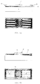
- Figure 1a represents a bolometer wherein porous silicon regions 11 has been formed on a substrate 10
- figure 1b represents the deposition and the patterning of an insulating layer 12 on the substrate 10
- a polycrystalline Si-Ge layer 13 is then deposited and patterned in order to form the supports 15 connected to the substrate at the anchor points 14 and the active area 16 as represented in figure 1c.
- figure 1c has to be considered only as an example and the present invention is not limited to this particular shape, but covers all similar structures, characterised by long and thin supports.
- bolometers One of the most important applications of bolometers is the realisation of IR cameras.
- Said camera is an array of pixels, each containing a bolometer and some electronics.
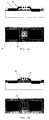
- FIG. 2 A schematic view of a pixel is shown in figure 2.
- the bolometer is represented by the reference 21 , and is connected to a CMOS switch 22 , built in the substrate, while the signal and gate lines 23 and 24 go to the external read-out. Externally to the array, a voltage waveform generator 25 and a load resistor 26 are provided.
- the CMOS switch 22 is closed, a short voltage pulse is sent to the bolometer, and the voltage drop across the load resistance is measured. This operation is repeated in presence of IR radiation.
- a signal is defined as the difference of the voltage across the load resistor measured with and without IR light. Note that in a normal operation, the duration of the voltage pulse is shorter than the thermal time constant of the bolometer, and does not originate a temperature increase.
- the volt responsivity i.e. the signal per unit incident power, is given by: where R L and R B are respectively the load and bolometer resistance.
- the noise which affects this signal has two contributions : external (from read-out electronics, load resistor, amplifiers%) and internal (due to the bolometer itself). External noise can be reduced by design optimisation and is to a good extent independent of the bolometer characteristics. Concerning the bolometer noise, the relevant quantity is not the noise itself but the noise equivalent power (NEP), i.e. the power which generates a signal equal to the noise.
- NEP noise equivalent power
- Johnson noise it can be defined as :
- NEP th 4 kGT 2 ⁇ f t
- ⁇ f t is a thermal bandwidth of the order of the inverse of the thermal time constant of the bolometer.
- the material grown at atmospheric pressure has a relatively low compressive stress, and this stress is reduced to zero after an annealing at 900 °C for 30 minutes.
- poly-Si grown by low pressure chemical vapour deposition at 620 °C exhibits an internal compressive stress larger than 300 MPa, which is annealed out at a temperature of 1050°C.
- the material grown at reduced pressure (e.g. 40 torrs) has a tensile internal stress, which is almost insensitive to annealing.
- the above observations indicate that the internal stress of poly-SiGe can be tuned by appropriate choice of growing conditions and annealing temperatures. This allows to choose the stress of the active layer so as to compensate the one of the layers forming the IR absorber. By this procedure, low stress and mechanically stable structures can thus be obtained. Except that in the case of an IR absorber with very low tensile stress, this compensation procedure requires low annealing temperature or even no annealing at all.
- thermal conductivity of poly-SiGe depends on the concentration of germanium atoms and is about 4 times lower than that of poly-Si for a germanium concentration of 30%. This reduction of thermal conductivity has obvious beneficial effects on the responsivity and on the noise equivalent power of the bolometer.
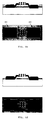
- the substrate is a silicon wafer, said substrate being already processed in order to form the appropriate CMOS switches and covered with standard passivation layers.
- a thin layer 42 (e.g. 100 nm thick) is deposited onto the above substrate 41 , in order to serve as etch stop during the etching of the sacrificial layer 43 .
- This layer 42 can be according to a first preferred embodiment a silicon-rich silicon nitride or any other material which is resistant to the etching agent of the sacrificial layer.
- the thin layer 42 can be an undoped poly-Si layer.
- the sacrificial layer 43 (1 or 2 ⁇ m of TEOS) is then deposited and patterned by standard lithography. Typical lateral dimension of the remaining TEOS regions vary from 20 ⁇ m to 50 ⁇ m.
- the poly-SiGe active layer 44 (0.5 ⁇ m or 0.3 ⁇ m thick) is deposited in a chemical vapour deposition system at a temperature comprised between 600°C - 700°C and preferably around 650°C at atmospheric or at reduced pressure.
- Gases used for the deposition are diclorosilane and germane. Their relative proportion is chosen in such a way that the concentration of germanium in the film is about 30%. This is the concentration which minimises the thermal conductivity.
- the nucleation of poly-SiGe on oxides is slow, then a thin (30 ⁇ ) nucleation layer of poly-Si is used. It is also possible to use a mixture of silane and germane. In this case, no nucleation layer will be necessary.
- silicon nitride 45 is deposited. It will serve for electrical insulation of the absorber from the active element.
- the stack of these two layers is then patterned.
- the holes 46 on the active layer will be useful during the sacrificial layer etching.
- the contacts 47 drawn in figure 4b are large and useful for testing single devices. When the device is inserted in a matrix their dimension can be reduced.
- the contacts 47 and the supports 48 are implanted with a high boron dose and the active area with a moderate dose.
- implanting the active area by a low doping dose it is also possible to dope it at a desired level during the deposition of poly-SiGe by adding appropriate gases to diclorosilane and germane. An annealing for dopant activation and diffusion is performed.
- the supports act as electrical contacts and the conductivity and the TCR of the active area is tuned to the desired value.
- the construction of the bolometer proceeds by the deposition and patterning of the absorber 49 as represented in figure 4d. It is composed, for example, by a triple layer: starting from the silicon nitride 45 , a metal reflector 51 , an insulating layer 52 about 1.5 ⁇ m thick, and a semitransparent metal 53 are formed. Other possibilities for preparing the absorber exists and can be used. They are generally known to the man skilled in the art.
- the construction of the bolometer is completed by the removal of the sacrificial layer using standard micro machining techniques (see figure 4f). Values of resistivity and temperature coefficient of resistance for different implanted doses of boron and for different annealing temperature.
Landscapes
- Engineering & Computer Science (AREA)
- Mechanical Engineering (AREA)
- Manufacturing & Machinery (AREA)
- Microelectronics & Electronic Packaging (AREA)
- Physics & Mathematics (AREA)
- General Physics & Mathematics (AREA)
- Spectroscopy & Molecular Physics (AREA)
- Photometry And Measurement Of Optical Pulse Characteristics (AREA)
- Radiation Pyrometers (AREA)
- Physical Vapour Deposition (AREA)
- Light Receiving Elements (AREA)
Priority Applications (13)
| Application Number | Priority Date | Filing Date | Title |
|---|---|---|---|
| EP97870044A EP0867701A1 (en) | 1997-03-28 | 1997-03-28 | Method of fabrication of an infrared radiation detector and more particularly an infrared sensitive bolometer |
| EP02077978A EP1263056A3 (en) | 1997-03-28 | 1998-03-26 | Method of controlling stress in a polycrystalline SiGe layer deposited on a substrate |
| DE69811968T DE69811968T2 (de) | 1997-03-28 | 1998-03-26 | Herstellungsverfahren für einen infrarotempfindlichen Strahlungsdetektor, insbesondere einen infrarotempfindlichen Bolometer |
| EP98870058A EP0867702B1 (en) | 1997-03-28 | 1998-03-26 | Method of fabrication of an infrared radiation detector and more particularly an infrared sensitive bolometer |
| US09/049,797 US6194722B1 (en) | 1997-03-28 | 1998-03-27 | Method of fabrication of an infrared radiation detector and infrared detector device |
| JP10122633A JPH1140824A (ja) | 1997-03-28 | 1998-03-27 | 赤外線輻射検出器、特に赤外線検出ボロメータ、の製造法 |
| US09/702,501 US6274462B1 (en) | 1997-03-28 | 2000-10-31 | Method of fabrication of an infrared radiation detector and infrared detector device |
| US09/816,611 US6707121B2 (en) | 1997-03-28 | 2001-03-23 | Micro electro mechanical systems and devices |
| US09/861,334 US6884636B2 (en) | 1997-03-28 | 2001-05-18 | Method of fabrication of an infrared radiation detector and infrared detector device |
| US10/263,623 US7176111B2 (en) | 1997-03-28 | 2002-10-03 | Method for depositing polycrystalline SiGe suitable for micromachining and devices obtained thereof |
| US10/921,012 US7075081B2 (en) | 1997-03-28 | 2004-08-17 | Method of fabrication of an infrared radiation detector and infrared detector device |
| US11/418,973 US7320896B2 (en) | 1997-03-28 | 2006-05-05 | Infrared radiation detector |
| JP2007029141A JP2007165927A (ja) | 1997-03-28 | 2007-02-08 | 基板上に積層する多結晶シリコンゲルマニウム層中の内部応力を制御する方法 |
Applications Claiming Priority (1)
| Application Number | Priority Date | Filing Date | Title |
|---|---|---|---|
| EP97870044A EP0867701A1 (en) | 1997-03-28 | 1997-03-28 | Method of fabrication of an infrared radiation detector and more particularly an infrared sensitive bolometer |
Publications (1)
| Publication Number | Publication Date |
|---|---|
| EP0867701A1 true EP0867701A1 (en) | 1998-09-30 |
Family
ID=8230989
Family Applications (3)
| Application Number | Title | Priority Date | Filing Date |
|---|---|---|---|
| EP97870044A Withdrawn EP0867701A1 (en) | 1997-03-28 | 1997-03-28 | Method of fabrication of an infrared radiation detector and more particularly an infrared sensitive bolometer |
| EP02077978A Withdrawn EP1263056A3 (en) | 1997-03-28 | 1998-03-26 | Method of controlling stress in a polycrystalline SiGe layer deposited on a substrate |
| EP98870058A Expired - Lifetime EP0867702B1 (en) | 1997-03-28 | 1998-03-26 | Method of fabrication of an infrared radiation detector and more particularly an infrared sensitive bolometer |
Family Applications After (2)
| Application Number | Title | Priority Date | Filing Date |
|---|---|---|---|
| EP02077978A Withdrawn EP1263056A3 (en) | 1997-03-28 | 1998-03-26 | Method of controlling stress in a polycrystalline SiGe layer deposited on a substrate |
| EP98870058A Expired - Lifetime EP0867702B1 (en) | 1997-03-28 | 1998-03-26 | Method of fabrication of an infrared radiation detector and more particularly an infrared sensitive bolometer |
Country Status (4)
| Country | Link |
|---|---|
| US (5) | US6194722B1 (enExample) |
| EP (3) | EP0867701A1 (enExample) |
| JP (2) | JPH1140824A (enExample) |
| DE (1) | DE69811968T2 (enExample) |
Cited By (6)
| Publication number | Priority date | Publication date | Assignee | Title |
|---|---|---|---|---|
| WO2001074708A3 (en) * | 2000-04-05 | 2002-03-21 | Imec Inter Uni Micro Electr | Method for depositing polycrystalline sige suitable for micromachining and devices obtained thereof |
| US7176111B2 (en) | 1997-03-28 | 2007-02-13 | Interuniversitair Microelektronica Centrum (Imec) | Method for depositing polycrystalline SiGe suitable for micromachining and devices obtained thereof |
| CN101832831A (zh) * | 2010-04-22 | 2010-09-15 | 无锡市纳微电子有限公司 | 一种压阻传感器芯片及其制作方法 |
| EP2181463A4 (en) * | 2007-08-22 | 2012-03-28 | Drs Rsta Inc | PIXEL STRUCTURE WITH UMBRELLA-TYPE ABSORBENT WITH ONE OR MORE DIMENSIONED CHANNELS OR CHANNELS TO INCREASE RADIATION ABSORPTION |
| CN104614086A (zh) * | 2015-03-06 | 2015-05-13 | 上海新微技术研发中心有限公司 | 气压式温度传感器及其制作方法 |
| CN106653940A (zh) * | 2016-11-21 | 2017-05-10 | 深圳信息职业技术学院 | 张应变锗msm光电探测器及其制备方法 |
Families Citing this family (99)
| Publication number | Priority date | Publication date | Assignee | Title |
|---|---|---|---|---|
| EP0867701A1 (en) * | 1997-03-28 | 1998-09-30 | Interuniversitair Microelektronica Centrum Vzw | Method of fabrication of an infrared radiation detector and more particularly an infrared sensitive bolometer |
| EP1136440A1 (en) * | 2000-03-24 | 2001-09-26 | Interuniversitair Micro-Elektronica Centrum Vzw | Method of improving mechanical strenghtin micro electro mechanical systems and devices produced thereof |
| ATE283549T1 (de) * | 1997-06-24 | 2004-12-15 | Massachusetts Inst Technology | Kontrolle der verspannungsdichte durch verwendung von gradientenschichten und durch planarisierung |
| US7227176B2 (en) * | 1998-04-10 | 2007-06-05 | Massachusetts Institute Of Technology | Etch stop layer system |
| CN1118103C (zh) * | 1998-10-21 | 2003-08-13 | 李韫言 | 微细加工热辐射红外传感器 |
| AU3346000A (en) * | 1999-01-15 | 2000-08-01 | Regents Of The University Of California, The | Polycrystalline silicon germanium films for forming micro-electromechanical systems |
| JP2001153720A (ja) * | 1999-11-30 | 2001-06-08 | Nec Corp | 熱型赤外線検出器 |
| CN1217417C (zh) * | 1999-12-10 | 2005-08-31 | 株式会社半导体能源研究所 | 半导体器件及其制造方法 |
| JP2001264441A (ja) * | 2000-01-14 | 2001-09-26 | Seiko Instruments Inc | カロリーメーターとその製造方法 |
| US6750130B1 (en) | 2000-01-20 | 2004-06-15 | Amberwave Systems Corporation | Heterointegration of materials using deposition and bonding |
| JP2003520444A (ja) * | 2000-01-20 | 2003-07-02 | アンバーウェーブ システムズ コーポレイション | 高温成長を不要とする低貫通転位密度格子不整合エピ層 |
| US6602613B1 (en) | 2000-01-20 | 2003-08-05 | Amberwave Systems Corporation | Heterointegration of materials using deposition and bonding |
| WO2001063232A1 (en) * | 2000-02-24 | 2001-08-30 | University Of Virginia Patent Foundation | High sensitivity infrared sensing apparatus and related method thereof |
| EP1251099A3 (en) * | 2000-03-24 | 2004-07-21 | Interuniversitair Microelektronica Centrum Vzw | Method of improving mechanical strength in micro electro mechanical systems and devices produced thereof |
| US7078321B2 (en) | 2000-06-19 | 2006-07-18 | Semiconductor Energy Laboratory Co., Ltd. | Semiconductor device and method of manufacturing the same |
| AU2001283138A1 (en) | 2000-08-07 | 2002-02-18 | Amberwave Systems Corporation | Gate technology for strained surface channel and strained buried channel mosfet devices |
| DE60125952T2 (de) * | 2000-08-16 | 2007-08-02 | Massachusetts Institute Of Technology, Cambridge | Verfahren für die herstellung eines halbleiterartikels mittels graduellem epitaktischen wachsen |
| US20020100942A1 (en) * | 2000-12-04 | 2002-08-01 | Fitzgerald Eugene A. | CMOS inverter and integrated circuits utilizing strained silicon surface channel MOSFETs |
| US6649480B2 (en) | 2000-12-04 | 2003-11-18 | Amberwave Systems Corporation | Method of fabricating CMOS inverter and integrated circuits utilizing strained silicon surface channel MOSFETs |
| DE10102993B4 (de) * | 2001-01-24 | 2009-01-08 | Robert Bosch Gmbh | Herstellungsverfahren für ein mikromechanisches Bauelement |
| US6703688B1 (en) | 2001-03-02 | 2004-03-09 | Amberwave Systems Corporation | Relaxed silicon germanium platform for high speed CMOS electronics and high speed analog circuits |
| US6830976B2 (en) * | 2001-03-02 | 2004-12-14 | Amberwave Systems Corproation | Relaxed silicon germanium platform for high speed CMOS electronics and high speed analog circuits |
| US6724008B2 (en) | 2001-03-02 | 2004-04-20 | Amberwave Systems Corporation | Relaxed silicon germanium platform for high speed CMOS electronics and high speed analog circuits |
| US6723661B2 (en) * | 2001-03-02 | 2004-04-20 | Amberwave Systems Corporation | Relaxed silicon germanium platform for high speed CMOS electronics and high speed analog circuits |
| US6489616B2 (en) * | 2001-03-19 | 2002-12-03 | The Board Of Governors Of Southwest Missouri State University | Doped, organic carbon-containing sensor for infrared detection and a process for the preparation thereof |
| US6940089B2 (en) | 2001-04-04 | 2005-09-06 | Massachusetts Institute Of Technology | Semiconductor device structure |
| US7057256B2 (en) | 2001-05-25 | 2006-06-06 | President & Fellows Of Harvard College | Silicon-based visible and near-infrared optoelectric devices |
| US7442629B2 (en) | 2004-09-24 | 2008-10-28 | President & Fellows Of Harvard College | Femtosecond laser-induced formation of submicrometer spikes on a semiconductor substrate |
| AU2002322105A1 (en) * | 2001-06-14 | 2003-01-02 | Amberware Systems Corporation | Method of selective removal of sige alloys |
| FR2827707B1 (fr) * | 2001-07-20 | 2003-11-21 | Fr De Detecteurs Infrarouges S | Procede de realisation d'un detecteur bolometrique et detecteur realise selon ce procede |
| WO2003025984A2 (en) | 2001-09-21 | 2003-03-27 | Amberwave Systems Corporation | Semiconductor structures employing strained material layers with defined impurity gradients and methods for fabricating same |
| AU2002341803A1 (en) | 2001-09-24 | 2003-04-07 | Amberwave Systems Corporation | Rf circuits including transistors having strained material layers |
| WO2003045837A2 (en) * | 2001-11-26 | 2003-06-05 | Wisconsin Alumni Research Foundation | Stress control of semiconductor microstructures for thin film growth |
| US6780786B2 (en) * | 2001-11-26 | 2004-08-24 | The Regents Of The University Of California | Method for producing a porous silicon film |
| US6793389B2 (en) * | 2002-02-04 | 2004-09-21 | Delphi Technologies, Inc. | Monolithically-integrated infrared sensor |
| AU2003222003A1 (en) | 2002-03-14 | 2003-09-29 | Amberwave Systems Corporation | Methods for fabricating strained layers on semiconductor substrates |
| US6767751B2 (en) * | 2002-05-28 | 2004-07-27 | Silicon Light Machines, Inc. | Integrated driver process flow |
| FI114658B (fi) | 2002-06-03 | 2004-11-30 | Metorex Internat Oy | Suprajohtava antennikytketty kuumapistemikrobolometri, menetelmät sellaisen valmistamiseksi ja käyttämiseksi sekä bolometrinen kuvantamisjärjestely |
| US7307273B2 (en) * | 2002-06-07 | 2007-12-11 | Amberwave Systems Corporation | Control of strain in device layers by selective relaxation |
| US20030227057A1 (en) * | 2002-06-07 | 2003-12-11 | Lochtefeld Anthony J. | Strained-semiconductor-on-insulator device structures |
| US7615829B2 (en) * | 2002-06-07 | 2009-11-10 | Amberwave Systems Corporation | Elevated source and drain elements for strained-channel heterojuntion field-effect transistors |
| US7335545B2 (en) * | 2002-06-07 | 2008-02-26 | Amberwave Systems Corporation | Control of strain in device layers by prevention of relaxation |
| US6995430B2 (en) * | 2002-06-07 | 2006-02-07 | Amberwave Systems Corporation | Strained-semiconductor-on-insulator device structures |
| US7074623B2 (en) * | 2002-06-07 | 2006-07-11 | Amberwave Systems Corporation | Methods of forming strained-semiconductor-on-insulator finFET device structures |
| WO2003105206A1 (en) * | 2002-06-10 | 2003-12-18 | Amberwave Systems Corporation | Growing source and drain elements by selecive epitaxy |
| US6982474B2 (en) * | 2002-06-25 | 2006-01-03 | Amberwave Systems Corporation | Reacted conductive gate electrodes |
| US7375385B2 (en) | 2002-08-23 | 2008-05-20 | Amberwave Systems Corporation | Semiconductor heterostructures having reduced dislocation pile-ups |
| US7594967B2 (en) * | 2002-08-30 | 2009-09-29 | Amberwave Systems Corporation | Reduction of dislocation pile-up formation during relaxed lattice-mismatched epitaxy |
| US7210653B2 (en) * | 2002-10-22 | 2007-05-01 | The Boeing Company | Electric-based secondary power system architectures for aircraft |
| WO2004068556A2 (en) | 2003-01-27 | 2004-08-12 | Amberwave Systems Corporation | Semiconductor structures with structural homogeneity |
| WO2004081982A2 (en) * | 2003-03-07 | 2004-09-23 | Amberwave Systems Corporation | Shallow trench isolation process |
| FR2864065B1 (fr) * | 2003-12-22 | 2006-02-24 | Univ Toulouse | Utilisation de ferrites spinelles comme materiau sensible pour dispositifs bolometriques de detection de l'infrarouge. |
| US7393733B2 (en) | 2004-12-01 | 2008-07-01 | Amberwave Systems Corporation | Methods of forming hybrid fin field-effect transistor structures |
| US20060113603A1 (en) * | 2004-12-01 | 2006-06-01 | Amberwave Systems Corporation | Hybrid semiconductor-on-insulator structures and related methods |
| KR100827314B1 (ko) * | 2005-10-10 | 2008-05-06 | 삼성전기주식회사 | 열처리에 의해 평탄면을 가지는 멤스 소자 및 광변조기제조 방법 |
| US20080085334A1 (en) * | 2006-10-10 | 2008-04-10 | Husky Injection Molding Systems Ltd. | Hot Runner System Sensor |
| US20080185522A1 (en) * | 2007-02-06 | 2008-08-07 | Shih-Chia Chang | Infrared sensors and methods for manufacturing the infrared sensors |
| US7795605B2 (en) * | 2007-06-29 | 2010-09-14 | International Business Machines Corporation | Phase change material based temperature sensor |
| US20100203243A1 (en) * | 2007-12-27 | 2010-08-12 | Applied Materials, Inc. | Method for forming a polysilicon film |
| WO2010127298A2 (en) * | 2009-04-30 | 2010-11-04 | Sionyx, Inc. | Low oxygen content semiconductor material for surface enhanced photonic devices associated methods |
| US20100320548A1 (en) * | 2009-06-18 | 2010-12-23 | Analog Devices, Inc. | Silicon-Rich Nitride Etch Stop Layer for Vapor HF Etching in MEMS Device Fabrication |
| US20110203648A1 (en) * | 2009-08-20 | 2011-08-25 | James Carey | Laser processed heterojunction photovoltaic devices and associated methods |
| US8476598B1 (en) | 2009-08-31 | 2013-07-02 | Sionyx, Inc. | Electromagnetic radiation imaging devices and associated methods |
| US8309389B1 (en) | 2009-09-10 | 2012-11-13 | Sionyx, Inc. | Photovoltaic semiconductor devices and associated methods |
| US8657227B1 (en) | 2009-09-11 | 2014-02-25 | The Boeing Company | Independent power generation in aircraft |
| US9911781B2 (en) | 2009-09-17 | 2018-03-06 | Sionyx, Llc | Photosensitive imaging devices and associated methods |
| US9673243B2 (en) | 2009-09-17 | 2017-06-06 | Sionyx, Llc | Photosensitive imaging devices and associated methods |
| US8476681B2 (en) | 2009-09-17 | 2013-07-02 | Sionyx, Inc. | Photosensitive imaging devices and associated methods |
| EP2478560A4 (en) * | 2009-09-17 | 2014-06-18 | Sionyx Inc | LIGHT-SENSITIVE IMAGING DEVICES AND CORRESPONDING METHODS |
| US20110095387A1 (en) * | 2009-10-22 | 2011-04-28 | James Carey | Semiconductor devices having an enhanced absorption region and associated methods |
| JP5644120B2 (ja) * | 2010-01-26 | 2014-12-24 | セイコーエプソン株式会社 | 熱型光検出器、熱型光検出装置、電子機器および熱型光検出器の製造方法 |
| US8692198B2 (en) | 2010-04-21 | 2014-04-08 | Sionyx, Inc. | Photosensitive imaging devices and associated methods |
| MD340Z (ro) * | 2010-04-23 | 2011-09-30 | Институт Электронной Инженерии И Промышленных Технологий | Bolometru |
| CN106449684B (zh) | 2010-06-18 | 2019-09-27 | 西奥尼克斯公司 | 高速光敏设备及相关方法 |
| US8738268B2 (en) | 2011-03-10 | 2014-05-27 | The Boeing Company | Vehicle electrical power management and distribution |
| US9496308B2 (en) | 2011-06-09 | 2016-11-15 | Sionyx, Llc | Process module for increasing the response of backside illuminated photosensitive imagers and associated methods |
| CN103946867A (zh) | 2011-07-13 | 2014-07-23 | 西奥尼克斯公司 | 生物计量成像装置和相关方法 |
| US9151597B2 (en) | 2012-02-13 | 2015-10-06 | First Solar, Inc. | In situ substrate detection for a processing system using infrared detection |
| US9064764B2 (en) | 2012-03-22 | 2015-06-23 | Sionyx, Inc. | Pixel isolation elements, devices, and associated methods |
| JP6466346B2 (ja) | 2013-02-15 | 2019-02-06 | サイオニクス、エルエルシー | アンチブルーミング特性を有するハイダイナミックレンジcmos画像センサおよび関連づけられた方法 |
| WO2014151093A1 (en) | 2013-03-15 | 2014-09-25 | Sionyx, Inc. | Three dimensional imaging utilizing stacked imager devices and associated methods |
| US9209345B2 (en) | 2013-06-29 | 2015-12-08 | Sionyx, Inc. | Shallow trench textured regions and associated methods |
| DE102014112672B4 (de) | 2014-09-03 | 2018-05-09 | Snaptrack, Inc. | Abdeckung für ein Bauelement und Verfahren zur Herstellung einer Abdeckung für ein Bauelement |
| US9864138B2 (en) | 2015-01-05 | 2018-01-09 | The Research Foundation For The State University Of New York | Integrated photonics including germanium |
| US9915567B2 (en) * | 2016-06-28 | 2018-03-13 | Excelitas Technologies Singapore Pte. Ltd. | Unreleased thermopile infrared sensor using material transfer method |
| US10976491B2 (en) | 2016-11-23 | 2021-04-13 | The Research Foundation For The State University Of New York | Photonics interposer optoelectronics |
| US10698156B2 (en) | 2017-04-27 | 2020-06-30 | The Research Foundation For The State University Of New York | Wafer scale bonded active photonics interposer |
| TWI646672B (zh) | 2017-12-01 | 2019-01-01 | 財團法人工業技術研究院 | 紅外線感測元件及其製造方法 |
| US10424608B1 (en) | 2018-01-31 | 2019-09-24 | Hrl Laboratories, Llc | Fabrication of polycrystalline semiconductor infrared detector |
| US10490689B1 (en) | 2018-01-31 | 2019-11-26 | Hrl Laboratories, Llc | Grain boundary passivation of polycrystalline materials |
| EP3776074B1 (en) | 2018-04-04 | 2023-11-22 | The Research Foundation for the State University of New York | Heterogeneous structure on an integrated photonics platform |
| US10816724B2 (en) | 2018-04-05 | 2020-10-27 | The Research Foundation For The State University Of New York | Fabricating photonics structure light signal transmission regions |
| TWI851601B (zh) | 2018-11-21 | 2024-08-11 | 紐約州立大學研究基金會 | 光子光電系統及其製造方法 |
| US11550099B2 (en) | 2018-11-21 | 2023-01-10 | The Research Foundation For The State University Of New York | Photonics optoelectrical system |
| US11029466B2 (en) | 2018-11-21 | 2021-06-08 | The Research Foundation For The State University Of New York | Photonics structure with integrated laser |
| CN113015889B (zh) * | 2019-02-28 | 2024-04-02 | 松下知识产权经营株式会社 | 红外线传感器、红外线传感器阵列及红外线传感器的制造方法 |
| KR20220086548A (ko) | 2019-06-18 | 2022-06-23 | 더 리서치 파운데이션 포 더 스테이트 유니버시티 오브 뉴욕 | 포토닉스 구조 도전성 광 경로 제조 |
| JP7309138B2 (ja) * | 2020-12-25 | 2023-07-18 | 国立大学法人横浜国立大学 | 赤外線吸収体および赤外線吸収体を備えるガスセンサ |
| TWI825710B (zh) | 2022-05-10 | 2023-12-11 | 財團法人工業技術研究院 | 紅外線元件及其製造方法 |
Citations (2)
| Publication number | Priority date | Publication date | Assignee | Title |
|---|---|---|---|---|
| WO1993013561A1 (en) * | 1991-12-20 | 1993-07-08 | Honeywell Inc. | Method of fabricating integrated infrared sensitive bolometers |
| US5367167A (en) * | 1991-09-30 | 1994-11-22 | Texas Instruments Incorporated | Uncooled infrared detector and method for forming the same |
Family Cites Families (49)
| Publication number | Priority date | Publication date | Assignee | Title |
|---|---|---|---|---|
| US4239312A (en) * | 1978-11-29 | 1980-12-16 | Hughes Aircraft Company | Parallel interconnect for planar arrays |
| US5220188A (en) | 1983-07-06 | 1993-06-15 | Honeywell Inc. | Integrated micromechanical sensor element |
| US5220189A (en) | 1983-07-06 | 1993-06-15 | Honeywell Inc. | Micromechanical thermoelectric sensor element |
| JPH0664906B2 (ja) * | 1984-11-30 | 1994-08-22 | キヤノン株式会社 | 固体メモリ− |
| US5300915A (en) * | 1986-07-16 | 1994-04-05 | Honeywell Inc. | Thermal sensor |
| US4902894A (en) * | 1986-09-26 | 1990-02-20 | Honeywell Inc. | Gate coupled input circuit |
| JPS63121851A (ja) * | 1986-11-11 | 1988-05-25 | Canon Inc | 電子写真用光受容部材 |
| US5010251A (en) * | 1988-08-04 | 1991-04-23 | Hughes Aircraft Company | Radiation detector array using radiation sensitive bridges |
| US5021663B1 (en) * | 1988-08-12 | 1997-07-01 | Texas Instruments Inc | Infrared detector |
| US5286976A (en) | 1988-11-07 | 1994-02-15 | Honeywell Inc. | Microstructure design for high IR sensitivity |
| CA2081306C (en) * | 1990-04-26 | 2000-07-18 | Kevin Charles Liddiard | Semiconductor film bolometer thermal infrared detector |
| US5291055A (en) * | 1992-01-28 | 1994-03-01 | The United States Of America As Represented By The Administrator Of National Aeronautics And Space Administration | Resonant infrared detector with substantially unit quantum efficiency |
| US5357803A (en) * | 1992-04-08 | 1994-10-25 | Rochester Institute Of Technology | Micromachined microaccelerometer for measuring acceleration along three axes |
| US5241193A (en) | 1992-05-19 | 1993-08-31 | Motorola, Inc. | Semiconductor device having a thin-film transistor and process |
| WO1993026050A1 (en) | 1992-06-11 | 1993-12-23 | Honeywell Inc. | Two-level microbridge bolometer imaging array and method of making same |
| US5444302A (en) * | 1992-12-25 | 1995-08-22 | Hitachi, Ltd. | Semiconductor device including multi-layer conductive thin film of polycrystalline material |
| US5371035A (en) * | 1993-02-01 | 1994-12-06 | Motorola Inc. | Method for forming electrical isolation in an integrated circuit device |
| ATE269588T1 (de) * | 1993-02-04 | 2004-07-15 | Cornell Res Foundation Inc | Mikrostrukturen und einzelmask, einkristall- herstellungsverfahren |
| US5396280A (en) * | 1993-02-26 | 1995-03-07 | International Business Machines, Corporation | Analog video processing apparatus and method for eliminating background levels in the analog signal |
| US5426070A (en) * | 1993-05-26 | 1995-06-20 | Cornell Research Foundation, Inc. | Microstructures and high temperature isolation process for fabrication thereof |
| US5399897A (en) | 1993-11-29 | 1995-03-21 | Raytheon Company | Microstructure and method of making such structure |
| US5883564A (en) * | 1994-04-18 | 1999-03-16 | General Motors Corporation | Magnetic field sensor having high mobility thin indium antimonide active layer on thin aluminum indium antimonide buffer layer |
| US5858819A (en) * | 1994-06-15 | 1999-01-12 | Seiko Epson Corporation | Fabrication method for a thin film semiconductor device, the thin film semiconductor device itself, liquid crystal display, and electronic device |
| JP2615429B2 (ja) * | 1994-09-13 | 1997-05-28 | 工業技術院長 | 3次元立体形状の創成法 |
| WO1996015550A1 (en) * | 1994-11-10 | 1996-05-23 | Lawrence Semiconductor Research Laboratory, Inc. | Silicon-germanium-carbon compositions and processes thereof |
| JP2674545B2 (ja) * | 1995-01-20 | 1997-11-12 | 日本電気株式会社 | 赤外線検出器及びその駆動方法 |
| JPH08261832A (ja) * | 1995-03-20 | 1996-10-11 | Fujitsu Ltd | 赤外線センサ及びその製造方法 |
| JP3287173B2 (ja) * | 1995-04-07 | 2002-05-27 | 三菱電機株式会社 | 赤外線検出素子 |
| JPH08335707A (ja) * | 1995-06-08 | 1996-12-17 | Nippondenso Co Ltd | 半導体力学量センサ及びその製造方法 |
| US6211560B1 (en) * | 1995-06-16 | 2001-04-03 | The United States Of America As Represented By The Secretary Of The Air Force | Voltage tunable schottky diode photoemissive infrared detector |
| JPH0953980A (ja) * | 1995-08-18 | 1997-02-25 | Nikon Corp | 熱型赤外線センサ |
| US5919364A (en) | 1996-06-24 | 1999-07-06 | Regents Of The University Of California | Microfabricated filter and shell constructed with a permeable membrane |
| GB9619706D0 (en) | 1996-09-20 | 1996-11-06 | Pharmacia Spa | Synergistic immunosuppressant composition containing a 2,2'-bi-1H-pyrrole comp und |
| US6707121B2 (en) * | 1997-03-28 | 2004-03-16 | Interuniversitair Microelektronica Centrum (Imec Vzw) | Micro electro mechanical systems and devices |
| EP0867701A1 (en) * | 1997-03-28 | 1998-09-30 | Interuniversitair Microelektronica Centrum Vzw | Method of fabrication of an infrared radiation detector and more particularly an infrared sensitive bolometer |
| FR2765245B1 (fr) | 1997-06-25 | 1999-09-17 | France Telecom | Procede d'obtention d'une couche de silicium-germanium polycristallin sur un substrat et son application a la microelectronique |
| US6689211B1 (en) * | 1999-04-09 | 2004-02-10 | Massachusetts Institute Of Technology | Etch stop layer system |
| US6238581B1 (en) | 1998-12-18 | 2001-05-29 | Eastman Kodak Company | Process for manufacturing an electro-mechanical grating device |
| US6534381B2 (en) | 1999-01-08 | 2003-03-18 | Silicon Genesis Corporation | Method for fabricating multi-layered substrates |
| AU3346000A (en) * | 1999-01-15 | 2000-08-01 | Regents Of The University Of California, The | Polycrystalline silicon germanium films for forming micro-electromechanical systems |
| US6822304B1 (en) * | 1999-11-12 | 2004-11-23 | The Board Of Trustees Of The Leland Stanford Junior University | Sputtered silicon for microstructures and microcavities |
| US6346453B1 (en) * | 2000-01-27 | 2002-02-12 | Sige Microsystems Inc. | Method of producing a SI-GE base heterojunction bipolar device |
| EP1251099A3 (en) * | 2000-03-24 | 2004-07-21 | Interuniversitair Microelektronica Centrum Vzw | Method of improving mechanical strength in micro electro mechanical systems and devices produced thereof |
| DE60139610D1 (de) * | 2000-04-05 | 2009-10-01 | Imec | Verfahren zum abscheiden eines zur mikrobearbeitung geeigneten polykristallinen sige |
| JP2003007629A (ja) * | 2001-04-03 | 2003-01-10 | Canon Inc | シリコン系膜の形成方法、シリコン系膜および半導体素子 |
| US6587613B2 (en) * | 2001-07-24 | 2003-07-01 | Innovative Technology Licensing, Llc | Hybrid MEMS fabrication method and new optical MEMS device |
| US6875671B2 (en) * | 2001-09-12 | 2005-04-05 | Reveo, Inc. | Method of fabricating vertical integrated circuits |
| US6666979B2 (en) * | 2001-10-29 | 2003-12-23 | Applied Materials, Inc. | Dry etch release of MEMS structures |
| US6770569B2 (en) * | 2002-08-01 | 2004-08-03 | Freescale Semiconductor, Inc. | Low temperature plasma Si or SiGe for MEMS applications |
-
1997
- 1997-03-28 EP EP97870044A patent/EP0867701A1/en not_active Withdrawn
-
1998
- 1998-03-26 EP EP02077978A patent/EP1263056A3/en not_active Withdrawn
- 1998-03-26 EP EP98870058A patent/EP0867702B1/en not_active Expired - Lifetime
- 1998-03-26 DE DE69811968T patent/DE69811968T2/de not_active Expired - Lifetime
- 1998-03-27 JP JP10122633A patent/JPH1140824A/ja active Pending
- 1998-03-27 US US09/049,797 patent/US6194722B1/en not_active Expired - Lifetime
-
2000
- 2000-10-31 US US09/702,501 patent/US6274462B1/en not_active Expired - Lifetime
-
2001
- 2001-05-18 US US09/861,334 patent/US6884636B2/en not_active Expired - Lifetime
-
2004
- 2004-08-17 US US10/921,012 patent/US7075081B2/en not_active Expired - Lifetime
-
2006
- 2006-05-05 US US11/418,973 patent/US7320896B2/en not_active Expired - Fee Related
-
2007
- 2007-02-08 JP JP2007029141A patent/JP2007165927A/ja active Pending
Patent Citations (2)
| Publication number | Priority date | Publication date | Assignee | Title |
|---|---|---|---|---|
| US5367167A (en) * | 1991-09-30 | 1994-11-22 | Texas Instruments Incorporated | Uncooled infrared detector and method for forming the same |
| WO1993013561A1 (en) * | 1991-12-20 | 1993-07-08 | Honeywell Inc. | Method of fabricating integrated infrared sensitive bolometers |
Non-Patent Citations (4)
| Title |
|---|
| GERWEN VAN P ET AL: "THIN-FILM BORON-DOPED POLYCRYSTALLINE SILICON 70%-GERMANIUM 30% FOR THERMOPILES", SENSORS AND ACTUATORS A, vol. A53, no. 1/03, May 1996 (1996-05-01), pages 325 - 328, XP000620316 * |
| STEINER P ET AL: "MICROMACHINING APPLICATIONS OF POROUS SILICON", THIN SOLID FILMS, vol. 255, no. 1/02, 15 January 1995 (1995-01-15), pages 52 - 58, XP000607762 * |
| SYUN-MING JANG ET AL: "THERMAL STABILITY OF SI/SI1-XGEX/SI HETEROSTRUCTURES DEPOSITED BY VERY LOW PRESSURE CHEMICAL VAPOR DEPOSITION", APPLIED PHYSICS LETTERS, vol. 61, no. 3, 20 July 1992 (1992-07-20), pages 315 - 317, XP000287677 * |
| UNEWISSE M H ET AL: "The growth and properties of semiconductor bolometers for infrared detection", GROWTH AND CHARACTERIZATION OF MATERIALS FOR INFRARED DETECTORS II, SAN DIEGO, CA, USA, 13-14 JULY 1995, vol. 2554, ISSN 0277-786X, PROCEEDINGS OF THE SPIE - THE INTERNATIONAL SOCIETY FOR OPTICAL ENGINEERING, 1995, SPIE-INT. SOC. OPT. ENG, USA, pages 43 - 54, XP002039425 * |
Cited By (7)
| Publication number | Priority date | Publication date | Assignee | Title |
|---|---|---|---|---|
| US7176111B2 (en) | 1997-03-28 | 2007-02-13 | Interuniversitair Microelektronica Centrum (Imec) | Method for depositing polycrystalline SiGe suitable for micromachining and devices obtained thereof |
| WO2001074708A3 (en) * | 2000-04-05 | 2002-03-21 | Imec Inter Uni Micro Electr | Method for depositing polycrystalline sige suitable for micromachining and devices obtained thereof |
| EP2181463A4 (en) * | 2007-08-22 | 2012-03-28 | Drs Rsta Inc | PIXEL STRUCTURE WITH UMBRELLA-TYPE ABSORBENT WITH ONE OR MORE DIMENSIONED CHANNELS OR CHANNELS TO INCREASE RADIATION ABSORPTION |
| CN101832831A (zh) * | 2010-04-22 | 2010-09-15 | 无锡市纳微电子有限公司 | 一种压阻传感器芯片及其制作方法 |
| CN101832831B (zh) * | 2010-04-22 | 2015-01-28 | 无锡市纳微电子有限公司 | 一种压阻传感器芯片及其制作方法 |
| CN104614086A (zh) * | 2015-03-06 | 2015-05-13 | 上海新微技术研发中心有限公司 | 气压式温度传感器及其制作方法 |
| CN106653940A (zh) * | 2016-11-21 | 2017-05-10 | 深圳信息职业技术学院 | 张应变锗msm光电探测器及其制备方法 |
Also Published As
| Publication number | Publication date |
|---|---|
| EP0867702B1 (en) | 2003-03-12 |
| US20050012040A1 (en) | 2005-01-20 |
| JP2007165927A (ja) | 2007-06-28 |
| US7075081B2 (en) | 2006-07-11 |
| US7320896B2 (en) | 2008-01-22 |
| DE69811968D1 (de) | 2003-04-17 |
| DE69811968T2 (de) | 2003-12-11 |
| EP1263056A2 (en) | 2002-12-04 |
| US6274462B1 (en) | 2001-08-14 |
| EP1263056A3 (en) | 2003-12-03 |
| US6194722B1 (en) | 2001-02-27 |
| US20060289764A1 (en) | 2006-12-28 |
| EP0867702A2 (en) | 1998-09-30 |
| US20010055833A1 (en) | 2001-12-27 |
| EP0867702A3 (en) | 1998-10-21 |
| JPH1140824A (ja) | 1999-02-12 |
| US6884636B2 (en) | 2005-04-26 |
Similar Documents
| Publication | Publication Date | Title |
|---|---|---|
| EP0867701A1 (en) | Method of fabrication of an infrared radiation detector and more particularly an infrared sensitive bolometer | |
| US5059543A (en) | Method of manufacturing thermopile infrared detector | |
| US5100479A (en) | Thermopile infrared detector with semiconductor supporting rim | |
| Unewisse et al. | Growth and properties of semiconductor bolometers for infrared detection | |
| US5369280A (en) | Semiconductor film bolometer thermal infrared detector | |
| US5288649A (en) | Method for forming uncooled infrared detector | |
| US5850098A (en) | Uncooled amorphous YBaCuO thin film infrared detector | |
| EP1417151B1 (en) | Method for the fabrication of suspended porous silicon microstructures and application in gas sensors | |
| EP0534768B1 (en) | Uncooled infrared detector and method for forming the same | |
| Almasri et al. | Self-supporting uncooled infrared microbolometers with low-thermal mass | |
| CA2182041C (en) | Infrared detector and fabrication method thereof | |
| Iborra et al. | IR uncooled bolometers based on amorphous Ge/sub x/Si/sub 1-x/O/sub y/on silicon micromachined structures | |
| US20040053435A1 (en) | Electronic device and method for fabricating the electronic device | |
| EP2995916A1 (en) | Surface micro-machined infrared sensor using highly temperature stable interferometric absorber | |
| Travers et al. | Fabrication of semiconducting YBaCuO surface-micromachined bolometer arrays | |
| Witvrouw et al. | Poly-SiGe, a superb material for MEMS | |
| JP4865957B2 (ja) | 熱型赤外線固体撮像装置の製造方法 | |
| Tezcan et al. | Uncooled microbolometer infrared focal plane array in standard CMOS | |
| Unewisse et al. | Semiconductor film bolometer technology for uncooled IR sensors | |
| Foote et al. | Transition edge YBa2Cu3O7-x microbolometers for infrared staring arrays | |
| AU641766B2 (en) | Semiconductor film bolometer thermal infrared detector | |
| Piotrowski et al. | Micromachined thermal devices-detectors and emitters | |
| CN112563403A (zh) | 一种低噪声热电堆器件的制作方法 | |
| Rana et al. | Amorphous Ge x Si 1-x O y: H Microbolometers with High Responsivity | |
| Heredia-J et al. | A boron doped amorphous silicon thin-film bolometer for long wavelength detection |
Legal Events
| Date | Code | Title | Description |
|---|---|---|---|
| PUAI | Public reference made under article 153(3) epc to a published international application that has entered the european phase |
Free format text: ORIGINAL CODE: 0009012 |
|
| 17P | Request for examination filed |
Effective date: 19970414 |
|
| AK | Designated contracting states |
Kind code of ref document: A1 Designated state(s): AT BE CH DE DK ES FI FR GB GR IE IT LI LU MC NL PT SE |
|
| AX | Request for extension of the european patent |
Free format text: AL;LT;LV;RO;SI |
|
| AKX | Designation fees paid | ||
| STAA | Information on the status of an ep patent application or granted ep patent |
Free format text: STATUS: THE APPLICATION IS DEEMED TO BE WITHDRAWN |
|
| 18D | Application deemed to be withdrawn |
Effective date: 19990331 |