EP0853431B1 - Dispositif de traitement de signal - Google Patents
Dispositif de traitement de signal Download PDFInfo
- Publication number
- EP0853431B1 EP0853431B1 EP98200025A EP98200025A EP0853431B1 EP 0853431 B1 EP0853431 B1 EP 0853431B1 EP 98200025 A EP98200025 A EP 98200025A EP 98200025 A EP98200025 A EP 98200025A EP 0853431 B1 EP0853431 B1 EP 0853431B1
- Authority
- EP
- European Patent Office
- Prior art keywords
- data
- circuit
- quantization
- signal processing
- block
- Prior art date
- Legal status (The legal status is an assumption and is not a legal conclusion. Google has not performed a legal analysis and makes no representation as to the accuracy of the status listed.)
- Expired - Lifetime
Links
Images


Classifications
-
- H—ELECTRICITY
- H04—ELECTRIC COMMUNICATION TECHNIQUE
- H04N—PICTORIAL COMMUNICATION, e.g. TELEVISION
- H04N5/00—Details of television systems
- H04N5/76—Television signal recording
- H04N5/91—Television signal processing therefor
- H04N5/92—Transformation of the television signal for recording, e.g. modulation, frequency changing; Inverse transformation for playback
- H04N5/926—Transformation of the television signal for recording, e.g. modulation, frequency changing; Inverse transformation for playback by pulse code modulation
- H04N5/9265—Transformation of the television signal for recording, e.g. modulation, frequency changing; Inverse transformation for playback by pulse code modulation with processing of the sound signal
- H04N5/9267—Transformation of the television signal for recording, e.g. modulation, frequency changing; Inverse transformation for playback by pulse code modulation with processing of the sound signal using time division multiplex of the PCM audio and PCM video signals
-
- H—ELECTRICITY
- H04—ELECTRIC COMMUNICATION TECHNIQUE
- H04N—PICTORIAL COMMUNICATION, e.g. TELEVISION
- H04N5/00—Details of television systems
- H04N5/76—Television signal recording
- H04N5/91—Television signal processing therefor
- H04N5/92—Transformation of the television signal for recording, e.g. modulation, frequency changing; Inverse transformation for playback
- H04N5/926—Transformation of the television signal for recording, e.g. modulation, frequency changing; Inverse transformation for playback by pulse code modulation
- H04N5/9261—Transformation of the television signal for recording, e.g. modulation, frequency changing; Inverse transformation for playback by pulse code modulation involving data reduction
- H04N5/9264—Transformation of the television signal for recording, e.g. modulation, frequency changing; Inverse transformation for playback by pulse code modulation involving data reduction using transform coding
-
- H—ELECTRICITY
- H04—ELECTRIC COMMUNICATION TECHNIQUE
- H04N—PICTORIAL COMMUNICATION, e.g. TELEVISION
- H04N5/00—Details of television systems
- H04N5/76—Television signal recording
- H04N5/91—Television signal processing therefor
- H04N5/92—Transformation of the television signal for recording, e.g. modulation, frequency changing; Inverse transformation for playback
- H04N5/926—Transformation of the television signal for recording, e.g. modulation, frequency changing; Inverse transformation for playback by pulse code modulation
- H04N5/9265—Transformation of the television signal for recording, e.g. modulation, frequency changing; Inverse transformation for playback by pulse code modulation with processing of the sound signal
-
- H—ELECTRICITY
- H04—ELECTRIC COMMUNICATION TECHNIQUE
- H04N—PICTORIAL COMMUNICATION, e.g. TELEVISION
- H04N5/00—Details of television systems
- H04N5/76—Television signal recording
- H04N5/91—Television signal processing therefor
- H04N5/93—Regeneration of the television signal or of selected parts thereof
- H04N5/94—Signal drop-out compensation
- H04N5/945—Signal drop-out compensation for signals recorded by pulse code modulation
Definitions
- the present invention relates to a signal processing apparatus, and more particularly to an improvement of recording or reproducing apparatus for a digital video tape recorder (D-VTR) for discrete cosine transforming (DCT) video signal in order to compress amount of information thereof and recording it.
- D-VTR digital video tape recorder
- DCT discrete cosine transforming
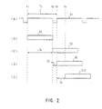
- Fig. 1 generally denotes the D-VTR.
- a digital video signal S1 (Fig. 2(B)) input from a predetermined video signal generating unit is input to a DCT shuffling circuit 2.
- the DCT shuffling circuit 2 has a DCT address circuit 3 in association therewith, a vertical synchronizing signal S V (Fig. 2(A)) is input to the DCT address circuit 3.
- the DCT shuffling circuit 2 divides the digital video signal S1 into DCT blocks of 8 columns x 4 rows for each one field by shuffle address generated by the DCT address circuit 3 on the basis of the vertical synchronizing signal S V .
- the DCT shuffling circuit 2 collects 10 blocks of the DCT blocks from their respective positions discretely located from each other within a screen to generate shuffle data S2 (Fig. 2(C)), and outputs the shuffle data S2 to the following DCT conversion circuit 4.
- the DCT shuffling circuit 2 performs shuffling processing by each one field.
- the shuffle data S2 output from the DCT shuffling circuit 2 is supplied to the DCT conversion circuit 4 at a timing delayed by one field time period T2 from the digital video signal S1 as shown in Fig. 2(C).
- the DCT conversion circuit 4 performs discrete cosine transform to data of each DCT block and supplies DCT data S3 to a quantization delay circuit 5 and a quantization level detecting circuit 6.
- the quantization level detecting circuit 6 detects a quantization level (quantization width) for achieving a target compression rate for the DCT data S3. Since, at this time, about ten-block time period is required as the signal processing time in the quantization level detecting circuit 6, the quantization delay circuit 5 delays the DCT data S3 by the signal processing time, and supplies it to a quantization circuit 7 as a quantization delay output data S5.
- the quantization delay output data S5 is input to the quantization circuit 7 at the same timing as quantization level data S4 which is output from the quantization level detecting circuit 6 at a time point t3 delayed by a 10-block time period T3 from the shuffle data S2 as shown in Fig. 2(D).
- the quantization circuit 7 quantizes the quantization delay output data S5 supplied from the quantization delay circuit 5 based on the quantization level data S4 supplied from the quantization level detecting circuit 6 in order to compress amount of information thereof. At this time, the quantization circuit 7 detects a maximum value, a minimum value, and a mean value etc., of quantization level within one field, on the basis of a period signal for each one field obtained from the vertical synchronizing signal S V at a vertical counter 8 provided in association therewith, and outputs the result as detection data S6 to a quantization monitor (not shown) to monitor the state of compression of data at the quantization circuit 7.
- quantization data S7 obtained from the quantization circuit 7 is supplied to a variable-length coding circuit 9.
- the variable-length coding circuit 9 performs variable-length coding to the quantization data S7 to generate variable-length coding data S9 having a block length prescribed in a format, and outputs it to an error correcting outer coding circuit 11.
- the error correcting outer coding circuit 11 generates an error correcting outer code for correcting an error occurred in the manner of a burst, on the basis of a timing obtained from the vertical synchronizing signal S V at a parity timing circuit 12 which is provided in association therewith, and the result is added to the variable-length coding data S9 and is output to a track shuffling circuit 13.
- the track shuffling circuit 13 generates track shuffle data S13 by recording the data into an order suitable for the track pattern on a magnetic tape, in accordance with shuffle address obtained from the vertical synchronizing signal S V at a track address circuit 14 which is provided in association therewith.
- the track shuffle data S13 is supplied to an error correcting inner coding circuit 15.
- the error correcting inner coding circuit 15 generates an error correcting inner code for correcting random error and adds to the track shuffle data S13.
- An ID counter 16 which is provided in association with the error correcting inner coding circuit 15, obtains a block number obtained from the vertical synchronizing signal S V and the color field signal S C , and color field information corresponding to a time period when the phase shift of carrier resulting from phase shifts by each scanning line completes a cycle.
- the error correcting inner coding circuit 15 adds the block number and the color field information to the track shuffle data S13 as ID information, and outputs the result to a recording circuit 17 as recording data S12.
- the recording circuit 17 converts the recording data S12 from an 8 [bit] parallel form to 1 [bit] serial form and effects channel coding suitable for magnetic recording, and records on a magnetic tape 19 by means of a magnetic head 18 provided on a rotary drum.
- the track shuffling circuit 13 since the track shuffling circuit 13 performs re-ordering processing of data by each 1/3 field, the recording data S12 obtained on the basis of the track shuffle data S13 is output from the error correcting inner coding circuit 15 at a time point t4 delayed by 1/3 field period T4 from quantization delay output data S5 output from the quantization delay circuit 5 as shown in Fig. 2(E).
- a synchronizing pattern is added to the beginning of a data block as a delimiter for the block and a delimiter for restoring data recorded in 1 [bit] serial form on the magnetic tape into the original 8 [bit] parallel form.
- a block number for indicating the sequential order of each data block is added as ID information at the error correcting inner coding circuit 15, so that an image is reproduced even when data blocks are not continuously reproduced as the reproducing head helically scans a plurality of tracks in double-speed reproducing etc. Furthermore, color field information is also added as ID information at the error correcting inner coding circuit 15.
- video data generated through the above DCT shuffling circuit 2 to the error correcting inner coding circuit 15 is recorded subsequently to the ID information.
- the quantization level information in data compression is added at the quantization circuit 7 in accordance with the quantization level data S4.
- an inner parity data for correcting a random error is added at the error correcting inner coding circuit 15.
- data is output with a delay of the time necessary for the signal processing at each signal processing circuit.
- data is output with a delay corresponding to one field time period T2 (Fig. 2(C)), and at the quantization delay circuit 5, data is delayed by 10-block time period T3 (Fig. 2(D)).
- the quantization circuit 7, and the variable-length coding circuit 9 data is delayed by about one block time period respectively, and at the track shuffling circuit 13, data is delayed by 1/3 field time period T4 (Fig. 2(E)).
- timing signals must be generated with their phase conforming to their respective delay time from the vertical synchronizing signal S V .
- EP-A-493,129 discloses an image processing method and apparatus which can transmit image data even on a transmission path of a bad quality.
- an analogue image signal is converted to digital data and is variable length compression coded.
- a sync code and transmission ID are added to the data train.
- Boundary information and parity information are then added to this data and blocks of data containing this information are transmitted.
- the present invention provides a video signal processing apparatus according to claim 1.
- the present invention provides a signal processing apparatus such that, data to be output with a delay at each signal processing circuit can securely be processed and delivered irrespective of delay time of the data due to the signal processing time of the respective signal processing circuit.
- a signal processing apparatus having a plurality of signal processing circuits which are sequentially connected so as to make a desired data into a predetermined unit and sequentially perform signal processing, at least one of which performs a predetermined signal processing to the desired data at the timing determined on the basis of a processing timing of the another signal processing circuits, wherein at least one of signal processing circuits outputs the desired data with adding timing data indicating the processing timing.
- the another signal processing circuits set the timing of signal processing for the desired data on the basis of the timing data.
- a signal processing apparatus having a plurality of signal processing circuits which are sequentially connected so as to make video data into a predetermined unit and sequentially perform signal processing, at least one of which performs predetermined signal processing to the video data at the timing determined on the basis of a processing timing of the another signal processing circuits, wherein at least one of signal processing circuits outputs the video data with adding timing data indicating the processing timing.
- the another signal processing circuits set the timing of signal processing for the video data on the basis of the timing data.
- a signal processing apparatus 20 for digital video signal for performing a predetermined signal processing for digital video signal S1 comprising: a block shuffling circuit 21 for making input digital video signal S1 into a predetermined unit in order to perform a block conversion coding and shuffling it to obtain shuffle data S21, and then for outputting the shuffle data S21 with adding a block number information D BL and a color field information D FI of the digital video signal S1 as header data; a block conversion coding circuit 23 receiving the output of the block shuffling circuit 21 for performing block conversion coding for the shuffle data S21 and obtain coding data S22, and for outputting the coded data S22 with adding the header data; a quantization circuit 25 receiving the output of the block conversion coding circuit 23 for quantizing the coding data S22 and obtain quantized data S25, and for outputting the quantized data S25 with adding the header data to which quantization level information D Q in quantizing is added to the quantized data S25;
- timing data D FI , D BL , and/or D Q are/is added to the data S1 and processing at each signal processing circuit 21 to 29 is performed at a timing based on the timing data D FI , D BL , and/or D Q , so that the data S1 can be delivered between the signal processing circuits 21 to 29 without regard to processing time in the respective signal processing circuits 21 to 29.
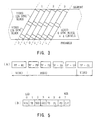
- Fig. 3 shows a recording format on a magnetic tape which is recorded by a D-VTR according to the present invention.
- Digital video signal and digital audio signal for one field are made into a predetermined unit and recorded in the area of six helical recording tracks.
- the six recording tracks are segmented by two recording tracks and at each of which the segment number 1, 2, 3 are sequentially allocated from the head of one field.
- the track number 0 or 1 is allocated to the two recording tracks of respective segment.
- a preamble, video data of 126 sync blocks, audio data of 6 sync blocks x 4 channels, and video data of 126 sync blocks are sequentially recorded.
- each sync block is 180-byte length, in which at the beginning 2 bytes, a synchronization pattern SYNC is recorded, at the succeeding 2 bytes, an identification pattern ID is recorded, at the succeeding 162 bytes, compressed video data, audio data, or these error correcting outer code parity is recorded as a recording data DATA, and at the end 14 bytes, an error correcting inner code parity IP of the identification pattern ID or recording data DATA is recorded.
- the value "2ED3(H)" is recorded as a fixed pattern.
- corresponding numbers of sync block are recorded as the identification pattern ID in the sequence of Fig. 5(A).
- flag information indicating the property of corresponding sync block is recorded as an identification pattern ID by sector numbers as shown in Fig. 5(B).
- bit 0 of the LSB in this byte indicates the sector of video data, and when being the value "0", which is an identification flag indicating the sector of audio data.
- bit 1 the value "0” or “1” is recorded as a track number in the above segment number.
- the value "1", “2”, or “3” of the above segment number is recorded in 2 bits.
- bit 4 the bit 7 of the MSB indicates a format of the digital video data, and when being component video data, the value "1" is recorded, and when being composite video data, the value "0" is recorded.
- a DCT address circuit 22 generates a shuffle address on the basis of the vertical synchronization signal S V , and a DCT shuffling circuit 21 shuffles digital video signal S1 in accordance with the shuffle address to generate shuffle data S21, and supplies it to a DCT circuit 23.
- the DCT shuffling circuit 21 adds a block number D BL generated by the DCT address circuit 22 and a color field information D FI to DCT block data D SH as header information.
- the block number D BL corresponds to the total of the sync block number of the first byte in the identification pattern ID which has been described accompanying with Figs. 4 and 5(A) and 5(B)
- the color field information D FI corresponds to the color field information of the bits 4 to 6 of the second byte.
- the DCT transformation circuit 23 performs discrete cosine transformation for respective DCT block data D SH on the basis of the block number D BL and color field information D FI , and supplies the result as DCT data S22 to a quantization level delay circuit 24.
- the quantization level delay circuit 24 detects a quantization level for determining a quantized width at the following quantization circuit 25 while delaying the DCT data S22, and as shown in Fig. 7(B), outputs the DCT data D DCT to a quantization circuit 25 as quantization level delay output data S23 with adding thus detected quantization level information D Q as a header information.
- the quantization circuit 25 quantizes the DCT data D DCT on the basis of the quantization level information D Q added as a header information in order to compress. At this time, the head and end of the field are investigated by the block number D BL added as a header information to calculate the mean value of the quantization levels, etc., the calculated result S24 is output to a quantization monitor (not shown), so that the compressed state can be monitored.
- the compression-processed quantized data S25 is supplied to a variable-length coding circuit 26 to be variable-length coded.
- variable-length coded data S26 is supplied to an error correcting outer coding circuit 27.
- the error correcting outer coding circuit 27 generates a parity timing from the block number D BL (Figs. 7(A) and 7(B)) which is in association with the variable-length coded data S26 as a header information to generate an error correcting outer code. Further, the following track shuffling circuit 28 also generates a shuffle address from the block number D BL (Figs. 7(A) and 7(B)) which is in association with the variable-length coded data S26 in order to re-order the data, and sends it to the following error correcting inner coding circuit 29 as track shuffle data S28.
- the error correcting inner coding circuit 29 generates an error correcting inner code, and adds the synchronization pattern SYNC to generate recording data S12 shown in Fig. 7(C).
- the recording data S12 is recorded on a magnetic tape 19 through the following recording circuit 30 and magnetic head 18.
- the error correcting inner coding circuit 19 since the block number D BL and field information D FI which are necessary as ID information, are previously added to the data as header information, it is unnecessary to add those again.
- reproduced data S31 which is reproduced through a reproducing head 31 and reproducing circuit 32 is input to a correcting circuit 33 to be correction-processed by using the error correcting inner code recorded with the recording data, and is output to a de-shuffling circuit 34.
- the de-shuffling circuit 34 de-shuffles the reproduced data re-ordered to the sequence corresponding to the track pattern on the magnetic tape into the original sequence, and outputs it to the following correcting circuit 35 as de-shuffle data S34.
- the correcting circuit 35 corrects an error in the manner of burst of the de-shuffle data S34 and outputs it to the following variable-length decoding circuit 36.
- the variable-length decoding circuit 36 obtains variable-length decoded data S35 from the de-shuffle data S34 and outputs it to an inverse-quantization circuit 37 to perform inverse-quantization processing.
- the inverse-quantization circuit 37 outputs thus obtained inverse-quantized data S37 to an IDCT circuit to perform inverse-transform processing for discrete cosine transformation at the DCT transforming circuit 23 described above.
- the IDCT circuit outputs thus obtained IDCT data S38 to the following de-shuffling circuit 39 to re-order the DCT-blocked data in the sequence of scanning, and outputs it as reproducing digital video signal S39.
- the D-VTR 20 adds the block number D BL and field number D FI to the digital video signal S1 as header information at the DCT shuffling circuit 21, and further adds the quantization level information D Q as a header information at the quantization level delay circuit 24.
- the header information information necessary for the signal processing can be obtained from only input data at each signal processing circuit, further the information is input at the same timing as the processing data.
- the header information is used as a timing information at each signal processing circuit, and signal processing is performed in accordance with the timing of the above header information, so that in each signal processing circuit, signal processing can be performed at the securely timing without regard to the processing delay time of signal processing circuits connected to the previous stage or latter stage. Therefore, in each signal processing circuit, a counter circuit for generating timing in respective signal processing, a latch circuit for timing phases by delaying the information, etc. can be omitted.
- the color field information D FI is added as a header information, so that the color field information D FI is delayed with the data at each signal processing circuit and transmitted to the last recording data S12. Further, also the quantization level information D Q detected at the quantization level delay circuit 24 is added to the data as a header information, so that at the quantization circuit 25 of next stage, the quantizing operation can be executed by investigating a quantization level from the header information.
- the timing necessary for respective signal processing is added for the data to be transmitted, as a header information, so that each signal processing circuit can be avoided to be complicated structure such that a circuit for obtaining the timing necessary for the signal processing is added at the respective signal processing circuits.
- each signal processing circuit the signal processing can be performed without generating a timing necessary for the signal processing at the respective signal processing circuits, so that the signal processing circuit can be developed without regard to delay time at each signal processing circuit. Therefore, even if processing time of each signal processing circuit is changed in its development process, the signal processing circuit provided to a latter stage of the above signal processing circuit may not be changed in accordance with the such changed time period, so can be developed more easily.
- the present invention is not only limited to this, but is widely applicable to a signal processing apparatus such that data is transmitted via a plurality of signal processing circuits.
- the present invention is being suitable to apply to a signal processing apparatus, for example, being a recording or reproducing apparatus for digital video tape recorder (DVTR) for discrete cosine transforming video signal in order to compress amount of information thereof and record.
- a signal processing apparatus for example, being a recording or reproducing apparatus for digital video tape recorder (DVTR) for discrete cosine transforming video signal in order to compress amount of information thereof and record.
- DVDTR digital video tape recorder
Landscapes
- Engineering & Computer Science (AREA)
- Multimedia (AREA)
- Signal Processing (AREA)
- Television Signal Processing For Recording (AREA)
- Compression Or Coding Systems Of Tv Signals (AREA)
- Communication Control (AREA)
- Time-Division Multiplex Systems (AREA)
Claims (7)
- Appareil de traitement de signal vidéo pour traiter un signal vidéo numérique d'entrée (S1, SC, SV), comprenant :
un premier moyen de traitement (21, 22) pour constituer des unités de bloc qui présentent une dimension prédéterminée à partir dudit signal vidéo numérique et pour additionner respectivement une information de numéro de bloc (DBL) qui indique l'ordre séquentiel desdites unités de bloc auxdites unités de bloc ;
caractérisé par :
un second moyen de traitement (23, 24) pour réaliser un codage par conversion de bloc sur lesdites unités de bloc afin de générer des données codées (S22) qui remplacent des données desdites unités de bloc en fonction de ladite information de numéro de bloc additionnée auxdites unités de bloc par ledit premier moyen de traitement. - Appareil de traitement de signal vidéo selon la revendication 1, dans lequel ledit second moyen de traitement (23, 24) inclut un moyen d'addition (24) pour additionner une information de niveau de quantification (DQ) qui indique une largeur de quantification desdites données codées.
- Appareil de traitement de signal vidéo selon la revendication 2, comprenant en outre un troisième moyen de traitement (25) connecté audit second moyen de traitement pour recevoir lesdites données codées, ladite information de numéro de bloc et ladite information de niveau de quantification, laquelle information est additionnée auxdites données codées en tant que données d'en-tête, pour quantifier lesdites données codées afin de générer des données de quantification (S25) en fonction de ladite information de numéro de bloc et de ladite information de niveau de quantification.
- Appareil de traitement de signal vidéo selon la revendication 3, dans lequel ledit troisième moyen de traitement (25) inclut un moyen pour calculer une valeur moyenne (S24) des niveaux de quantification sur la base de ladite information de numéro de bloc de telle sorte qu'un état de quantification puisse être surveillé.
- Appareil de traitement de signal vidéo selon la revendication 4, comprenant en outre un quatrième moyen de traitement (27) connecté audit troisième moyen de traitement pour recevoir lesdites données de quantification (S25) et ladite information de numéro de bloc (DBL) qui est additionnée auxdites données de quantification en tant qu'en-tête, pour générer des données de correction d'erreur (DP) conformément à une donnée de cadencement de parité qui est générée à partir de ladite information de numéro de bloc.
- Appareil de traitement de signal vidéo selon la revendication 1, dans lequel ladite information de numéro de bloc inclut des données de numéro de segment (SG0, SG1) et des données de numéro de piste (TR) qui indiquent une position d'enregistrement desdites données de quantification sur le support d'enregistrement.
- Appareil de traitement de signal vidéo selon la revendication 1, dans lequel :ledit premier moyen de traitement additionne une information de trame de couleur dudit signal vidéo numérique d'entrée auxdites unités de bloc ; etledit second moyen de traitement réalise ledit codage par conversion de bloc sur la base de ladite information de numéro de bloc et de ladite information de trame de couleur qui est additionnée auxdites unités de bloc dans ledit premier moyen de traitement.
Applications Claiming Priority (4)
| Application Number | Priority Date | Filing Date | Title |
|---|---|---|---|
| JP9685193 | 1993-03-31 | ||
| JP9685193 | 1993-03-31 | ||
| JP96851/93 | 1993-03-31 | ||
| EP94910554A EP0648051B1 (fr) | 1993-03-31 | 1994-03-29 | Processeur de signal |
Related Parent Applications (1)
| Application Number | Title | Priority Date | Filing Date |
|---|---|---|---|
| EP94910554A Division EP0648051B1 (fr) | 1993-03-31 | 1994-03-29 | Processeur de signal |
Publications (3)
| Publication Number | Publication Date |
|---|---|
| EP0853431A2 EP0853431A2 (fr) | 1998-07-15 |
| EP0853431A3 EP0853431A3 (fr) | 1998-08-26 |
| EP0853431B1 true EP0853431B1 (fr) | 2001-10-17 |
Family
ID=14175998
Family Applications (2)
| Application Number | Title | Priority Date | Filing Date |
|---|---|---|---|
| EP98200025A Expired - Lifetime EP0853431B1 (fr) | 1993-03-31 | 1994-03-29 | Dispositif de traitement de signal |
| EP94910554A Expired - Lifetime EP0648051B1 (fr) | 1993-03-31 | 1994-03-29 | Processeur de signal |
Family Applications After (1)
| Application Number | Title | Priority Date | Filing Date |
|---|---|---|---|
| EP94910554A Expired - Lifetime EP0648051B1 (fr) | 1993-03-31 | 1994-03-29 | Processeur de signal |
Country Status (6)
| Country | Link |
|---|---|
| US (3) | US5706056A (fr) |
| EP (2) | EP0853431B1 (fr) |
| JP (1) | JP3572324B2 (fr) |
| KR (1) | KR0148705B1 (fr) |
| DE (2) | DE69416372T2 (fr) |
| WO (1) | WO1994023534A1 (fr) |
Families Citing this family (3)
| Publication number | Priority date | Publication date | Assignee | Title |
|---|---|---|---|---|
| KR100660306B1 (ko) * | 1995-06-30 | 2007-03-28 | 소니 가부시끼 가이샤 | 데이터셔플링방법및그장치 |
| WO2004003897A1 (fr) * | 2002-07-01 | 2004-01-08 | Matsushita Electric Industrial Co., Ltd. | Disque optique, dispositif d'enregistrement de disque optique, procede d'enregistrement de disque optique |
| US8385424B2 (en) * | 2006-06-26 | 2013-02-26 | Qualcomm Incorporated | Reduction of errors during computation of inverse discrete cosine transform |
Family Cites Families (25)
| Publication number | Priority date | Publication date | Assignee | Title |
|---|---|---|---|---|
| US5194964A (en) * | 1988-09-15 | 1993-03-16 | Canon Kabushiki Kaisha | Apparatus for processing color or black and white video signals |
| EP0398741B1 (fr) * | 1989-05-19 | 1997-10-29 | Canon Kabushiki Kaisha | Système de transmission d'information d'image |
| JP3089475B2 (ja) * | 1989-06-21 | 2000-09-18 | ソニー株式会社 | ディジタル画像信号の符号化装置 |
| JPH03141752A (ja) * | 1989-10-27 | 1991-06-17 | Hitachi Ltd | 画像信号伝送方法 |
| JPH0468776A (ja) * | 1990-07-04 | 1992-03-04 | Pioneer Electron Corp | 情報記録及び静止画再生装置 |
| US5146324A (en) * | 1990-07-31 | 1992-09-08 | Ampex Corporation | Data compression using a feedforward quantization estimator |
| US5805302A (en) * | 1990-12-28 | 1998-09-08 | Canon Kabushiki Kaisha | Variable length encoding of image data |
| TW223690B (fr) * | 1991-02-13 | 1994-05-11 | Ampex | |
| JPH0541800A (ja) * | 1991-02-15 | 1993-02-19 | Olympus Optical Co Ltd | 画像復号化処理装置および復号化方法 |
| CA2062200A1 (fr) * | 1991-03-15 | 1992-09-16 | Stephen C. Purcell | Processeur de decompression pour applications video |
| US5220325A (en) * | 1991-03-28 | 1993-06-15 | At&T Bell Laboratories | Hierarchical variable length decoder for digital video data |
| JP3125451B2 (ja) * | 1991-11-05 | 2001-01-15 | ソニー株式会社 | 信号処理方法 |
| US5831679A (en) * | 1991-06-14 | 1998-11-03 | Wavephore, Inc. | Network for retrieval and video transmission of information |
| JPH0591494A (ja) * | 1991-09-26 | 1993-04-09 | Sony Corp | 高能率符号化装置 |
| US5349384A (en) * | 1992-01-14 | 1994-09-20 | Sony Corporation | Apparatus and methods for transmitting compressed digital image signals |
| JP3428033B2 (ja) * | 1992-02-19 | 2003-07-22 | 株式会社日立製作所 | ディジタルvtr |
| JPH05236427A (ja) * | 1992-02-25 | 1993-09-10 | Sony Corp | 画像信号の符号化装置及び符号化方法 |
| US5440344A (en) * | 1992-04-28 | 1995-08-08 | Mitsubishi Denki Kabushiki Kaisha | Video encoder using adjacent pixel difference for quantizer control |
| US5289577A (en) * | 1992-06-04 | 1994-02-22 | International Business Machines Incorporated | Process-pipeline architecture for image/video processing |
| JP3107826B2 (ja) * | 1992-06-16 | 2000-11-13 | サムスン エレクトロニクス カンパニー リミテッド | 逆互換性を有するhdtvの記録及び再生システム |
| US5289276A (en) * | 1992-06-19 | 1994-02-22 | General Electric Company | Method and apparatus for conveying compressed video data over a noisy communication channel |
| KR0134871B1 (ko) * | 1992-07-17 | 1998-04-22 | 사또오 후미오 | 고능률 부호화 복호화 시스템 |
| US5396497A (en) * | 1993-02-26 | 1995-03-07 | Sony Corporation | Synchronization of audio/video information |
| US5473385A (en) * | 1994-06-07 | 1995-12-05 | Tv/Com Technologies, Inc. | Clock correction in a video data decoder using video synchronization signals |
| JP3336754B2 (ja) * | 1994-08-19 | 2002-10-21 | ソニー株式会社 | デジタルビデオ信号の記録方法及び記録装置 |
-
1994
- 1994-03-29 KR KR1019940704409A patent/KR0148705B1/ko not_active IP Right Cessation
- 1994-03-29 DE DE69416372T patent/DE69416372T2/de not_active Expired - Fee Related
- 1994-03-29 EP EP98200025A patent/EP0853431B1/fr not_active Expired - Lifetime
- 1994-03-29 DE DE69428722T patent/DE69428722T2/de not_active Expired - Fee Related
- 1994-03-29 EP EP94910554A patent/EP0648051B1/fr not_active Expired - Lifetime
- 1994-03-29 WO PCT/JP1994/000503 patent/WO1994023534A1/fr active IP Right Grant
- 1994-03-29 JP JP52191494A patent/JP3572324B2/ja not_active Expired - Lifetime
- 1994-03-29 US US08/347,329 patent/US5706056A/en not_active Expired - Fee Related
-
1997
- 1997-06-05 US US08/869,592 patent/US6839385B1/en not_active Expired - Fee Related
- 1997-07-15 US US08/893,024 patent/US6704356B1/en not_active Expired - Fee Related
Also Published As
| Publication number | Publication date |
|---|---|
| US6704356B1 (en) | 2004-03-09 |
| DE69428722D1 (de) | 2001-11-22 |
| DE69416372T2 (de) | 1999-08-26 |
| DE69428722T2 (de) | 2002-06-20 |
| US6839385B1 (en) | 2005-01-04 |
| EP0853431A3 (fr) | 1998-08-26 |
| EP0648051A1 (fr) | 1995-04-12 |
| EP0853431A2 (fr) | 1998-07-15 |
| DE69416372D1 (de) | 1999-03-18 |
| EP0648051B1 (fr) | 1999-02-03 |
| US5706056A (en) | 1998-01-06 |
| KR0148705B1 (ko) | 1998-09-15 |
| WO1994023534A1 (fr) | 1994-10-13 |
| EP0648051A4 (fr) | 1995-04-19 |
| JP3572324B2 (ja) | 2004-09-29 |
Similar Documents
| Publication | Publication Date | Title |
|---|---|---|
| US6028726A (en) | Digital data recording/reproducing apparatus and method with means for adding arrival time to a data packet | |
| US4429334A (en) | Method for recording and reproducing a digital color video signal | |
| EP0599226B1 (fr) | Méthode pour copier des signaux vidéo numériques | |
| US5349384A (en) | Apparatus and methods for transmitting compressed digital image signals | |
| EP0553817B1 (fr) | Appareil de transfert d'informations digitales | |
| EP0853431B1 (fr) | Dispositif de traitement de signal | |
| US6429985B2 (en) | Digital information recording apparatus and digital information recording and reproducing apparatus | |
| JPH07226022A (ja) | ディジタル記録再生装置 | |
| US6393197B2 (en) | Digital video signal recording/reproducing apparatus and method thereof | |
| US6788877B1 (en) | Recording and reproducing apparatus | |
| US6438316B1 (en) | Recording/reproducing apparatus and method for including line numbers | |
| EP0772366B1 (fr) | Appareil d'enregistrement/de reproduction numérique | |
| US6724824B2 (en) | Digital signal processing method | |
| JP3105046B2 (ja) | 記録再生装置 | |
| JPH0520794A (ja) | デイジタル信号記録再生装置 | |
| JP2000132914A (ja) | データ処理装置およびデータ記録装置 | |
| JP3456601B2 (ja) | 映像記録装置、映像再生装置及びその方法 | |
| JP3956510B2 (ja) | 同期検出装置および方法、ならびに、再生装置 | |
| JP2000152187A (ja) | 同期検出装置および方法、ならびに、再生装置 | |
| JPH04329088A (ja) | ディジタル映像信号の符号化装置および復号化装置 | |
| JPS6314557B2 (fr) | ||
| JPH0583736A (ja) | 静止画記録再生装置 | |
| JPH04249992A (ja) | 磁気記録再生装置 |
Legal Events
| Date | Code | Title | Description |
|---|---|---|---|
| PUAI | Public reference made under article 153(3) epc to a published international application that has entered the european phase |
Free format text: ORIGINAL CODE: 0009012 |
|
| PUAL | Search report despatched |
Free format text: ORIGINAL CODE: 0009013 |
|
| AC | Divisional application: reference to earlier application |
Ref document number: 648051 Country of ref document: EP |
|
| AK | Designated contracting states |
Kind code of ref document: A2 Designated state(s): DE FR GB |
|
| AK | Designated contracting states |
Kind code of ref document: A3 Designated state(s): DE FR GB |
|
| 17P | Request for examination filed |
Effective date: 19990118 |
|
| 17Q | First examination report despatched |
Effective date: 19991014 |
|
| GRAG | Despatch of communication of intention to grant |
Free format text: ORIGINAL CODE: EPIDOS AGRA |
|
| GRAG | Despatch of communication of intention to grant |
Free format text: ORIGINAL CODE: EPIDOS AGRA |
|
| GRAH | Despatch of communication of intention to grant a patent |
Free format text: ORIGINAL CODE: EPIDOS IGRA |
|
| GRAH | Despatch of communication of intention to grant a patent |
Free format text: ORIGINAL CODE: EPIDOS IGRA |
|
| GRAA | (expected) grant |
Free format text: ORIGINAL CODE: 0009210 |
|
| RIN1 | Information on inventor provided before grant (corrected) |
Inventor name: UEDA, MAMORU |
|
| AC | Divisional application: reference to earlier application |
Ref document number: 648051 Country of ref document: EP |
|
| AK | Designated contracting states |
Kind code of ref document: B1 Designated state(s): DE FR GB |
|
| REF | Corresponds to: |
Ref document number: 69428722 Country of ref document: DE Date of ref document: 20011122 |
|
| REG | Reference to a national code |
Ref country code: GB Ref legal event code: IF02 |
|
| ET | Fr: translation filed | ||
| PLBE | No opposition filed within time limit |
Free format text: ORIGINAL CODE: 0009261 |
|
| STAA | Information on the status of an ep patent application or granted ep patent |
Free format text: STATUS: NO OPPOSITION FILED WITHIN TIME LIMIT |
|
| 26N | No opposition filed | ||
| PGFP | Annual fee paid to national office [announced via postgrant information from national office to epo] |
Ref country code: FR Payment date: 20030310 Year of fee payment: 10 |
|
| PGFP | Annual fee paid to national office [announced via postgrant information from national office to epo] |
Ref country code: GB Payment date: 20030326 Year of fee payment: 10 |
|
| PGFP | Annual fee paid to national office [announced via postgrant information from national office to epo] |
Ref country code: DE Payment date: 20030409 Year of fee payment: 10 |
|
| PG25 | Lapsed in a contracting state [announced via postgrant information from national office to epo] |
Ref country code: GB Free format text: LAPSE BECAUSE OF NON-PAYMENT OF DUE FEES Effective date: 20040329 |
|
| PG25 | Lapsed in a contracting state [announced via postgrant information from national office to epo] |
Ref country code: DE Free format text: LAPSE BECAUSE OF NON-PAYMENT OF DUE FEES Effective date: 20041001 |
|
| GBPC | Gb: european patent ceased through non-payment of renewal fee |
Effective date: 20040329 |
|
| PG25 | Lapsed in a contracting state [announced via postgrant information from national office to epo] |
Ref country code: FR Free format text: LAPSE BECAUSE OF NON-PAYMENT OF DUE FEES Effective date: 20041130 |
|
| REG | Reference to a national code |
Ref country code: FR Ref legal event code: ST |