EP0843895B1 - Method of manufacturing a metal interconnect structure for an integrated circuit with improved electromigration reliability - Google Patents
Method of manufacturing a metal interconnect structure for an integrated circuit with improved electromigration reliability Download PDFInfo
- Publication number
- EP0843895B1 EP0843895B1 EP96926850A EP96926850A EP0843895B1 EP 0843895 B1 EP0843895 B1 EP 0843895B1 EP 96926850 A EP96926850 A EP 96926850A EP 96926850 A EP96926850 A EP 96926850A EP 0843895 B1 EP0843895 B1 EP 0843895B1
- Authority
- EP
- European Patent Office
- Prior art keywords
- layer
- interconnect structure
- silicon
- deposited
- depositing
- Prior art date
- Legal status (The legal status is an assumption and is not a legal conclusion. Google has not performed a legal analysis and makes no representation as to the accuracy of the status listed.)
- Expired - Lifetime
Links
Images


Classifications
-
- H—ELECTRICITY
- H01—ELECTRIC ELEMENTS
- H01L—SEMICONDUCTOR DEVICES NOT COVERED BY CLASS H10
- H01L23/00—Details of semiconductor or other solid state devices
- H01L23/52—Arrangements for conducting electric current within the device in operation from one component to another, i.e. interconnections, e.g. wires, lead frames
-
- H—ELECTRICITY
- H01—ELECTRIC ELEMENTS
- H01L—SEMICONDUCTOR DEVICES NOT COVERED BY CLASS H10
- H01L21/00—Processes or apparatus adapted for the manufacture or treatment of semiconductor or solid state devices or of parts thereof
- H01L21/70—Manufacture or treatment of devices consisting of a plurality of solid state components formed in or on a common substrate or of parts thereof; Manufacture of integrated circuit devices or of parts thereof
- H01L21/71—Manufacture of specific parts of devices defined in group H01L21/70
- H01L21/768—Applying interconnections to be used for carrying current between separate components within a device comprising conductors and dielectrics
- H01L21/76838—Applying interconnections to be used for carrying current between separate components within a device comprising conductors and dielectrics characterised by the formation and the after-treatment of the conductors
- H01L21/76841—Barrier, adhesion or liner layers
- H01L21/76843—Barrier, adhesion or liner layers formed in openings in a dielectric
-
- H—ELECTRICITY
- H01—ELECTRIC ELEMENTS
- H01L—SEMICONDUCTOR DEVICES NOT COVERED BY CLASS H10
- H01L21/00—Processes or apparatus adapted for the manufacture or treatment of semiconductor or solid state devices or of parts thereof
- H01L21/02—Manufacture or treatment of semiconductor devices or of parts thereof
- H01L21/04—Manufacture or treatment of semiconductor devices or of parts thereof the devices having potential barriers, e.g. a PN junction, depletion layer or carrier concentration layer
- H01L21/18—Manufacture or treatment of semiconductor devices or of parts thereof the devices having potential barriers, e.g. a PN junction, depletion layer or carrier concentration layer the devices having semiconductor bodies comprising elements of Group IV of the Periodic Table or AIIIBV compounds with or without impurities, e.g. doping materials
- H01L21/28—Manufacture of electrodes on semiconductor bodies using processes or apparatus not provided for in groups H01L21/20 - H01L21/268
- H01L21/283—Deposition of conductive or insulating materials for electrodes conducting electric current
- H01L21/285—Deposition of conductive or insulating materials for electrodes conducting electric current from a gas or vapour, e.g. condensation
- H01L21/28506—Deposition of conductive or insulating materials for electrodes conducting electric current from a gas or vapour, e.g. condensation of conductive layers
- H01L21/28512—Deposition of conductive or insulating materials for electrodes conducting electric current from a gas or vapour, e.g. condensation of conductive layers on semiconductor bodies comprising elements of Group IV of the Periodic Table
-
- H—ELECTRICITY
- H01—ELECTRIC ELEMENTS
- H01L—SEMICONDUCTOR DEVICES NOT COVERED BY CLASS H10
- H01L21/00—Processes or apparatus adapted for the manufacture or treatment of semiconductor or solid state devices or of parts thereof
- H01L21/70—Manufacture or treatment of devices consisting of a plurality of solid state components formed in or on a common substrate or of parts thereof; Manufacture of integrated circuit devices or of parts thereof
- H01L21/71—Manufacture of specific parts of devices defined in group H01L21/70
- H01L21/768—Applying interconnections to be used for carrying current between separate components within a device comprising conductors and dielectrics
- H01L21/76838—Applying interconnections to be used for carrying current between separate components within a device comprising conductors and dielectrics characterised by the formation and the after-treatment of the conductors
- H01L21/76841—Barrier, adhesion or liner layers
- H01L21/7685—Barrier, adhesion or liner layers the layer covering a conductive structure
-
- H—ELECTRICITY
- H01—ELECTRIC ELEMENTS
- H01L—SEMICONDUCTOR DEVICES NOT COVERED BY CLASS H10
- H01L21/00—Processes or apparatus adapted for the manufacture or treatment of semiconductor or solid state devices or of parts thereof
- H01L21/70—Manufacture or treatment of devices consisting of a plurality of solid state components formed in or on a common substrate or of parts thereof; Manufacture of integrated circuit devices or of parts thereof
- H01L21/71—Manufacture of specific parts of devices defined in group H01L21/70
- H01L21/768—Applying interconnections to be used for carrying current between separate components within a device comprising conductors and dielectrics
- H01L21/76838—Applying interconnections to be used for carrying current between separate components within a device comprising conductors and dielectrics characterised by the formation and the after-treatment of the conductors
- H01L21/76877—Filling of holes, grooves or trenches, e.g. vias, with conductive material
-
- H—ELECTRICITY
- H01—ELECTRIC ELEMENTS
- H01L—SEMICONDUCTOR DEVICES NOT COVERED BY CLASS H10
- H01L23/00—Details of semiconductor or other solid state devices
- H01L23/52—Arrangements for conducting electric current within the device in operation from one component to another, i.e. interconnections, e.g. wires, lead frames
- H01L23/522—Arrangements for conducting electric current within the device in operation from one component to another, i.e. interconnections, e.g. wires, lead frames including external interconnections consisting of a multilayer structure of conductive and insulating layers inseparably formed on the semiconductor body
- H01L23/532—Arrangements for conducting electric current within the device in operation from one component to another, i.e. interconnections, e.g. wires, lead frames including external interconnections consisting of a multilayer structure of conductive and insulating layers inseparably formed on the semiconductor body characterised by the materials
- H01L23/53204—Conductive materials
- H01L23/53209—Conductive materials based on metals, e.g. alloys, metal silicides
- H01L23/53214—Conductive materials based on metals, e.g. alloys, metal silicides the principal metal being aluminium
- H01L23/53223—Additional layers associated with aluminium layers, e.g. adhesion, barrier, cladding layers
-
- H—ELECTRICITY
- H01—ELECTRIC ELEMENTS
- H01L—SEMICONDUCTOR DEVICES NOT COVERED BY CLASS H10
- H01L2924/00—Indexing scheme for arrangements or methods for connecting or disconnecting semiconductor or solid-state bodies as covered by H01L24/00
- H01L2924/0001—Technical content checked by a classifier
- H01L2924/0002—Not covered by any one of groups H01L24/00, H01L24/00 and H01L2224/00
Definitions
- the present invention relates generally to the interconnect structures contained within an integrated circuit device. More particularly, the present invention relates to a method of manufacturing a multilayer interconnect structure that uses layers of titanium, titanium nitride and aluminum-copper alloy to improve electromigration reliability.
- Integrated circuits generally comprise a semiconductor substrate upon which are formed various electronic components such as transistors, diodes and the like.
- Interconnect layers are formed on the semiconductor substrate to electrically interconnect the various electronic components to each other and to external components.
- the interconnect layers used on the semiconductor substrate have been made from polysilicon films, high temperature metal films, metal silicide films, aluminum films and aluminum alloy films.
- Each of these interconnect layers have an inherent resistance.
- the performance characteristics of highly integrated, high speed integrated circuits require that the resistance within the interconnect layers be held to a minimum.
- high speed integrated circuits typically use interconnect structures made of aluminum films or aluminum alloy films that have a relatively small resistivity as compared to the other interconnect structure choices.
- an objective of the present invention to provide an interconnect structure for an integrated circuit that prevents alloy spiking of the below lying substrate and has greatly improved electromigration reliability, thereby enabling integrated circuits that are more reliable, have higher performance rates and have increased ship density.
- a method of manufacturing a multilayer interconnect structure for a semiconductor integrated circuit comprising the steps of:
- the present invention relates to the production of a multilayer interconnect structure for use within an integrated circuit.
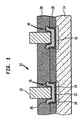
- a multilayer interconnect structure which has been produced in accordance with a preferred embodiment of the present invention is shown as part of an integrated circuit segment 12.
- the integrated circuit segment 12 includes a silicon-based substrate 14 upon which are disposed doped regions 16.
- An insulating oxide film 18 is deposited over the silicon-based substrate 14 leaving the doped regions 16 exposed.
- the multilayer interconnect structures 10 are deposited over the insulating oxide layer 18 and the exposed doped regions 16 of the silicon-based substrate 14.
- the multilayer interconnect structure 1 is comprised of a layer of titanium (Ti) 20, a layer of titanium nitride (TiN) 22, a layer of aluminum copper alloy 24 and a top layer of titanium nitride 26.
- the multilayer interconnect structures 10 are isolated from each other by a second oxide layer 28. Segments of a metal contact layer 32 extend through the second oxide layer 28 and contact the multilayer interconnect structures 10, thereby providing a means for electrically coupling the multilayer interconnect structures 10 to external components.
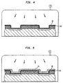
- Figs. 2 through 6 which also serve to illustrate an exemplary method according to the present invention of fabricating the multilayer interconnect structures 10.
- a silicon-based semiconductor substrate 14 is provided.
- the silicon-based substrate is selectively doped by conventional methods creating the doped regions 16.
- the doped regions 16 may be formed as part of a transistor structure or any other integrated component.
- An oxide layer 18 is deposited onto the silicon-based substrate 14 using tradition deposition techniques. The oxide layer 18 is selectively etched, thereby exposing the doped regions 16 on the silicon-based substrate 14.
- the silicon-based substrate 14 is placed within a clustered ultra-high vacuum (UHV) deposition system.
- UHV ultra-high vacuum
- the UHV deposition chamber 30 is evacuated to an ultra high vacuum where the pressure of oxygen and other reactive impurity gases within the UHV deposition chamber are reduced to below 10 -6 Pa.
- the silicon-based substrate 14 and oxide layer 18 are heated and cleaned of impurities within the UHV deposition chamber 30.
- the Ti layer 20 is deposited at a temperature between 150°C and 300°C.
- the TiN layer 22 is deposited in-situ within the same UHV deposition chamber 30 without release of the vacuum between the Ti deposition and the TiN deposition.
- the TiN layer 22 is preferably deposited at between 150°C and 350°C.
- a layer of aluminum alloy 24 is deposited over the TiN layer 22.
- the aluminum alloy layer 24 is Al-0.5% Cu.
- the aluminum alloy layer 24 is deposited at a thickness of approximately 1 ⁇ m, and deposition is conducted at a high temperature.
- the deposition of the aluminum alloy layer 24 is performed in the UHV deposition chamber 30 with no release of the ultra high vacuum between the TiN deposition and the aluminum alloy deposition.
- the aluminum alloy deposition is preferably performed at the highest temperature possible, given the temperature tolerances of the substrate 14, oxide layer 18, Ti layer 20 and TiN layer 22.
- the deposition temperature is preferably at least 350°C but preferably deposition should be performed near or about 550°C.
- a TiN antireflection layer 26 is deposited over the aluminum alloy layer 24, thereby completing the four layers of the interconnect structure 10.
- the TiN antireflection layer 26 is deposited in the same UHV deposition chamber 30 as are the other layers of the interconnect structure 10, without a release of the ultra high vacuum. Since the TiN layer 22 below the aluminum alloy layer 24 has already been deposited, the deposition source and targets already exist within the UHV deposition chamber 30 to deposit the TiN antireflection layer 26. This reduces the complexity and cost associated with manufacturing the overall interconnect structure 10.
- the Ti layer 20 is provided to function as a barrier metal layer between the aluminum alloy layer 24 and the silicon-based substrate 14.
- the Ti layer 20 alone while being a superior contact material in achieving a low resistance ohmic contact, does not act as a complete barrier to alloy spikes. If the Ti layer 20 alone were provided between the silicon-based substrate 14 and aluminum alloy layer 24, the titanium would react simultaneously with the silicon and the aluminum, so that alloy spikes into the silicon-based substrate eventually would occur. It is for this reason that the TiN layer 22 is provided between the Ti layer 20 and the aluminum alloy layer 24.
- the TiN layer 22 acts as a barrier metal to block aluminum diffusion along the grain boundaries in the aluminum alloy layer 24, thus preventing the growth of alloy spikes.
- the Ti layer 20 and the TiN layer 22 have a high resistance to electromigration and will constitute a current path even if the aluminum alloy layer 24 were to fail due to electromigration. As a result, a complete failure of the overall multilayer interconnect structure 10 is prevented.
- ELT electromigration lifetime
- sigma of the electromigration fail distribution are summarized for the seven test samples set forth in Table I.
- the test structures consist of M1 tungsten cap aluminum line, tapered vias (only one size allowed), and a RIE M2 line.
- the electromigration test-structure is designed to void the M2 near the Via 2, simulating the weakest point in normal product design.
- Electromigration Result ELT(hours)/sigma Test Sample Alloy M2V21 M2V23 M2V24 M2V22 1.2u 1 via 1.2u 4 via 3.8u 12 via 3.8u 3 via #1 AlCuTi 30/0.34 103/0.17 17/0.37 31/0.32 #2 AlCul%Si 31/0.22 147/0.11 15/0.21 39/0.18 #3 AlCu0.5%Si 36/0.18 138/0.27 12/0.28 25/0.23 #4 AlCu0.15%Si 32/0.20 128/0.14 12/0.20 32/0.21 #5 AlCu250C w/Ti 36/0.25 107/0.2 .13.5/0.2 34/0.2 #6 AlCul50C w/TIN 58/0.43 190/0.24 18/0.35 50/0.25 #7 AlCu350C w/TIN 81/0.35 450 61/0.33 116/0.26
- the electromigration life time (ELT) of an interconnect structure (sample #7) produced according to a preferred method embodying the present invention is between two times and four times as long as the other samples tested.
- the prior art does use Ti/TiN/aluminium alloy interconnect structures, the prior art does not deposit the aluminium alloy with in-situ UHV deposition at temperatures in excess of 300°C. Rather the prior art is more indicative of test sample #6, wherein Ti/TiN/aluminum alloy is deposited at low temperatures using traditional deposition techniques.
- the present invention test sample still has an ELT of between two times and four times greater than the other samples even though the same base materials are used.
- the interconnect structure 10 is etched and covered with an insulating second oxide layer 28.
- the second oxide layer 28 is then etched in the areas above where the interconnect structure 10 is to be engaged.
- a metal contact layer 32 is deposited upon the second oxide layer 28 and the exposed region of the interconnect structure 10.
- the metal contact layer 32 is then selectively etched, providing external contacts for coupling the underlying interconnect structure 10 to external components. Since the first TiN layer 22 under the aluminum alloy layer 24 has a thickness sufficient to prevent the growth of alloy spikes, the aluminum alloy layer 24 need not contain silicon. As a result, silicon does not precipitate in the metal contact layer 32 and the problems of silicon precipitation are avoided.
Landscapes
- Engineering & Computer Science (AREA)
- Physics & Mathematics (AREA)
- Condensed Matter Physics & Semiconductors (AREA)
- General Physics & Mathematics (AREA)
- Computer Hardware Design (AREA)
- Microelectronics & Electronic Packaging (AREA)
- Power Engineering (AREA)
- Manufacturing & Machinery (AREA)
- Internal Circuitry In Semiconductor Integrated Circuit Devices (AREA)
- Electrodes Of Semiconductors (AREA)
Applications Claiming Priority (3)
| Application Number | Priority Date | Filing Date | Title |
|---|---|---|---|
| US08/513,494 US5641992A (en) | 1995-08-10 | 1995-08-10 | Metal interconnect structure for an integrated circuit with improved electromigration reliability |
| US513494 | 1995-08-10 | ||
| PCT/US1996/012603 WO1997006562A1 (en) | 1995-08-10 | 1996-08-01 | Metal interconnect structure for an integrated circuit with improved electromigration reliability |
Publications (2)
| Publication Number | Publication Date |
|---|---|
| EP0843895A1 EP0843895A1 (en) | 1998-05-27 |
| EP0843895B1 true EP0843895B1 (en) | 2002-11-06 |
Family
ID=24043525
Family Applications (1)
| Application Number | Title | Priority Date | Filing Date |
|---|---|---|---|
| EP96926850A Expired - Lifetime EP0843895B1 (en) | 1995-08-10 | 1996-08-01 | Method of manufacturing a metal interconnect structure for an integrated circuit with improved electromigration reliability |
Country Status (6)
| Country | Link |
|---|---|
| US (2) | US5641992A (enExample) |
| EP (1) | EP0843895B1 (enExample) |
| JP (1) | JP2000501882A (enExample) |
| KR (1) | KR19990036191A (enExample) |
| DE (1) | DE69624712T2 (enExample) |
| WO (1) | WO1997006562A1 (enExample) |
Families Citing this family (27)
| Publication number | Priority date | Publication date | Assignee | Title |
|---|---|---|---|---|
| JPH09115829A (ja) * | 1995-10-17 | 1997-05-02 | Nissan Motor Co Ltd | アルミニウム配線部を有する半導体装置およびその製造方法 |
| US5994217A (en) * | 1996-12-16 | 1999-11-30 | Chartered Semiconductor Manufacturing Ltd. | Post metallization stress relief annealing heat treatment for ARC TiN over aluminum layers |
| US5943601A (en) * | 1997-04-30 | 1999-08-24 | International Business Machines Corporation | Process for fabricating a metallization structure |
| US5891802A (en) * | 1997-07-23 | 1999-04-06 | Advanced Micro Devices, Inc. | Method for fabricating a metallization stack structure to improve electromigration resistance and keep low resistivity of ULSI interconnects |
| US5942799A (en) * | 1997-11-20 | 1999-08-24 | Novellus Systems, Inc. | Multilayer diffusion barriers |
| KR100249047B1 (ko) | 1997-12-12 | 2000-03-15 | 윤종용 | 반도체 소자 및 그 제조 방법 |
| FR2774811B1 (fr) * | 1998-02-10 | 2003-05-09 | Sgs Thomson Microelectronics | Procede de formation de lignes conductrices sur des circuits integres |
| US5994219A (en) * | 1998-06-04 | 1999-11-30 | Taiwan Semiconductor Manufacturing Company, Ltd. | Add one process step to control the SI distribution of Alsicu to improved metal residue process window |
| TW439204B (en) * | 1998-09-18 | 2001-06-07 | Ibm | Improved-reliability damascene interconnects and process of manufacture |
| JP2000150520A (ja) * | 1998-11-10 | 2000-05-30 | Internatl Business Mach Corp <Ibm> | 相互接続部、及び相互接続部の製造方法 |
| US6777810B2 (en) * | 1999-02-19 | 2004-08-17 | Intel Corporation | Interconnection alloy for integrated circuits |
| US6352620B2 (en) | 1999-06-28 | 2002-03-05 | Applied Materials, Inc. | Staged aluminum deposition process for filling vias |
| US6433429B1 (en) * | 1999-09-01 | 2002-08-13 | International Business Machines Corporation | Copper conductive line with redundant liner and method of making |
| US6534404B1 (en) | 1999-11-24 | 2003-03-18 | Novellus Systems, Inc. | Method of depositing diffusion barrier for copper interconnect in integrated circuit |
| AU2003303784A1 (en) * | 2003-01-20 | 2004-08-13 | Systems On Silicon Manufacturing Company Pte Ltd | Titanium underlayer for lines in semiconductor devices |
| JP2004266039A (ja) * | 2003-02-28 | 2004-09-24 | Shin Etsu Handotai Co Ltd | 発光素子及び発光素子の製造方法 |
| US20040207093A1 (en) * | 2003-04-17 | 2004-10-21 | Sey-Shing Sun | Method of fabricating an alloy cap layer over CU wires to improve electromigration performance of CU interconnects |
| US6882924B2 (en) * | 2003-05-05 | 2005-04-19 | Precision Engine Controls Corp. | Valve flow control system and method |
| US7096450B2 (en) | 2003-06-28 | 2006-08-22 | International Business Machines Corporation | Enhancement of performance of a conductive wire in a multilayered substrate |
| KR100536808B1 (ko) * | 2004-06-09 | 2005-12-14 | 동부아남반도체 주식회사 | 반도체 소자 및 그 제조 방법 |
| US7339274B2 (en) * | 2004-08-17 | 2008-03-04 | Agere Systems Inc. | Metallization performance in electronic devices |
| US20090120785A1 (en) * | 2005-12-26 | 2009-05-14 | United Microelectronics Corp. | Method for forming metal film or stacked layer including metal film with reduced surface roughness |
| US20070144892A1 (en) * | 2005-12-26 | 2007-06-28 | Hui-Shen Shih | Method for forming metal film or stacked layer including metal film with reduced surface roughness |
| KR100650904B1 (ko) * | 2005-12-29 | 2006-11-28 | 동부일렉트로닉스 주식회사 | 알루미늄 배선 형성 방법 |
| US8003536B2 (en) * | 2009-03-18 | 2011-08-23 | International Business Machines Corporation | Electromigration resistant aluminum-based metal interconnect structure |
| CN102157356B (zh) * | 2011-03-15 | 2015-10-07 | 上海华虹宏力半导体制造有限公司 | 金属-绝缘体-金属半导体器件的下电极的制备方法 |
| US9851506B2 (en) * | 2015-06-04 | 2017-12-26 | Elenion Technologies, Llc | Back end of line process integrated optical device fabrication |
Family Cites Families (20)
| Publication number | Priority date | Publication date | Assignee | Title |
|---|---|---|---|---|
| US3879840A (en) * | 1969-01-15 | 1975-04-29 | Ibm | Copper doped aluminum conductive stripes and method therefor |
| US4926237A (en) * | 1988-04-04 | 1990-05-15 | Motorola, Inc. | Device metallization, device and method |
| US4998157A (en) * | 1988-08-06 | 1991-03-05 | Seiko Epson Corporation | Ohmic contact to silicon substrate |
| US5658828A (en) * | 1989-11-30 | 1997-08-19 | Sgs-Thomson Microelectronics, Inc. | Method for forming an aluminum contact through an insulating layer |
| US5478780A (en) * | 1990-03-30 | 1995-12-26 | Siemens Aktiengesellschaft | Method and apparatus for producing conductive layers or structures for VLSI circuits |
| JPH04116821A (ja) * | 1990-09-06 | 1992-04-17 | Fujitsu Ltd | 半導体装置の製造方法 |
| KR960001601B1 (ko) * | 1992-01-23 | 1996-02-02 | 삼성전자주식회사 | 반도체 장치의 접촉구 매몰방법 및 구조 |
| KR920010620A (ko) * | 1990-11-30 | 1992-06-26 | 원본미기재 | 다층 상호접속선을 위한 알루미늄 적층 접점/통로 형성방법 |
| US5345108A (en) * | 1991-02-26 | 1994-09-06 | Nec Corporation | Semiconductor device having multi-layer electrode wiring |
| DE4200809C2 (de) * | 1991-03-20 | 1996-12-12 | Samsung Electronics Co Ltd | Verfahren zur Bildung einer metallischen Verdrahtungsschicht in einem Halbleiterbauelement |
| US5270254A (en) * | 1991-03-27 | 1993-12-14 | Sgs-Thomson Microelectronics, Inc. | Integrated circuit metallization with zero contact enclosure requirements and method of making the same |
| JP2811131B2 (ja) * | 1991-04-26 | 1998-10-15 | 三菱電機株式会社 | 半導体装置の配線接続構造およびその製造方法 |
| EP0525517A1 (de) * | 1991-08-02 | 1993-02-03 | Siemens Aktiengesellschaft | Verfahren zur Auffüllung mindestens eines Kontaktloches in einer isolierenden Schicht |
| JPH0590203A (ja) * | 1991-09-27 | 1993-04-09 | Nec Corp | 半導体装置の製造方法 |
| US5240880A (en) * | 1992-05-05 | 1993-08-31 | Zilog, Inc. | Ti/TiN/Ti contact metallization |
| US5371042A (en) * | 1992-06-16 | 1994-12-06 | Applied Materials, Inc. | Method of filling contacts in semiconductor devices |
| US5270255A (en) * | 1993-01-08 | 1993-12-14 | Chartered Semiconductor Manufacturing Pte, Ltd. | Metallization process for good metal step coverage while maintaining useful alignment mark |
| US5378660A (en) * | 1993-02-12 | 1995-01-03 | Applied Materials, Inc. | Barrier layers and aluminum contacts |
| US5427666A (en) * | 1993-09-09 | 1995-06-27 | Applied Materials, Inc. | Method for in-situ cleaning a Ti target in a Ti + TiN coating process |
| JPH0786401A (ja) * | 1993-09-17 | 1995-03-31 | Fujitsu Ltd | 半導体装置の製造方法 |
-
1995
- 1995-08-10 US US08/513,494 patent/US5641992A/en not_active Expired - Lifetime
-
1996
- 1996-08-01 WO PCT/US1996/012603 patent/WO1997006562A1/en not_active Ceased
- 1996-08-01 EP EP96926850A patent/EP0843895B1/en not_active Expired - Lifetime
- 1996-08-01 JP JP9508537A patent/JP2000501882A/ja active Pending
- 1996-08-01 KR KR1019980700859A patent/KR19990036191A/ko not_active Ceased
- 1996-08-01 DE DE69624712T patent/DE69624712T2/de not_active Expired - Lifetime
-
1997
- 1997-04-29 US US08/841,030 patent/US5798301A/en not_active Expired - Lifetime
Also Published As
| Publication number | Publication date |
|---|---|
| US5798301A (en) | 1998-08-25 |
| DE69624712T2 (de) | 2003-09-11 |
| KR19990036191A (ko) | 1999-05-25 |
| WO1997006562A1 (en) | 1997-02-20 |
| JP2000501882A (ja) | 2000-02-15 |
| EP0843895A1 (en) | 1998-05-27 |
| US5641992A (en) | 1997-06-24 |
| DE69624712D1 (de) | 2002-12-12 |
Similar Documents
| Publication | Publication Date | Title |
|---|---|---|
| EP0843895B1 (en) | Method of manufacturing a metal interconnect structure for an integrated circuit with improved electromigration reliability | |
| US6255733B1 (en) | Metal-alloy interconnections for integrated circuits | |
| KR940010520B1 (ko) | 반도체장치 및 그 제조방법 | |
| US4985750A (en) | Semiconductor device using copper metallization | |
| US4912543A (en) | Integrated semiconductor circuit having an external contacting track level consisting of aluminum or of an aluminum alloy | |
| US5130274A (en) | Copper alloy metallurgies for VLSI interconnection structures | |
| JP3330495B2 (ja) | 電気的相互接続用薄膜金属バリア層 | |
| US5925933A (en) | Interconnect structure using Al2 -Cu for an integrated circuit chip | |
| US5286676A (en) | Methods of making integrated circuit barrier structures | |
| US4680612A (en) | Integrated semiconductor circuit including a tantalum silicide diffusion barrier | |
| US5567647A (en) | Method for fabricating a gate electrode structure of compound semiconductor device | |
| EP0542262B1 (en) | Method for forming a metal conductor in semiconductor device | |
| US5561083A (en) | Method of making multilayered Al-alloy structure for metal conductors | |
| US5238874A (en) | Fabrication method for laminated films comprising Al-Si-Co alloy film and refractory metal silioide copper film | |
| US5308792A (en) | Method for fabricating semiconductor device | |
| JP2600593B2 (ja) | 半導体装置およびその製造方法 | |
| JP3099406B2 (ja) | 集積回路の多層配線構造 | |
| JPH0653216A (ja) | 半導体装置およびその製造方法 | |
| JPH0629294A (ja) | 半導体装置の製造方法 | |
| EP1001463A2 (en) | Aluminum interconnects for integrated circuits comprising titanium under and overlayers | |
| JPH05102148A (ja) | 半導体装置 | |
| US5888899A (en) | Method for copper doping of aluminum films | |
| JPH05102154A (ja) | 半導体装置 | |
| KR100454629B1 (ko) | 반도체소자의도전배선형성방법 | |
| JPH07130849A (ja) | 半導体装置及びその製造方法 |
Legal Events
| Date | Code | Title | Description |
|---|---|---|---|
| PUAI | Public reference made under article 153(3) epc to a published international application that has entered the european phase |
Free format text: ORIGINAL CODE: 0009012 |
|
| 17P | Request for examination filed |
Effective date: 19980304 |
|
| AK | Designated contracting states |
Kind code of ref document: A1 Designated state(s): DE FR GB IE IT |
|
| 17Q | First examination report despatched |
Effective date: 19991202 |
|
| GRAG | Despatch of communication of intention to grant |
Free format text: ORIGINAL CODE: EPIDOS AGRA |
|
| RTI1 | Title (correction) |
Free format text: METHOD OF MANUFACTURING A METAL INTERCONNECT STRUCTURE FOR AN INTEGRATED CIRCUIT WITH IMPROVED ELECTROMIGRATION RELIABILITY |
|
| GRAG | Despatch of communication of intention to grant |
Free format text: ORIGINAL CODE: EPIDOS AGRA |
|
| GRAH | Despatch of communication of intention to grant a patent |
Free format text: ORIGINAL CODE: EPIDOS IGRA |
|
| GRAH | Despatch of communication of intention to grant a patent |
Free format text: ORIGINAL CODE: EPIDOS IGRA |
|
| GRAA | (expected) grant |
Free format text: ORIGINAL CODE: 0009210 |
|
| AK | Designated contracting states |
Kind code of ref document: B1 Designated state(s): DE FR GB IE IT |
|
| REG | Reference to a national code |
Ref country code: GB Ref legal event code: FG4D |
|
| REG | Reference to a national code |
Ref country code: IE Ref legal event code: FG4D |
|
| REF | Corresponds to: |
Ref document number: 69624712 Country of ref document: DE Date of ref document: 20021212 |
|
| RAP2 | Party data changed (patent owner data changed or rights of a patent transferred) |
Owner name: INTERNATIONAL BUSINESS MACHINES CORPORATION Owner name: INFINEON TECHNOLOGIES AG |
|
| ET | Fr: translation filed | ||
| PLBE | No opposition filed within time limit |
Free format text: ORIGINAL CODE: 0009261 |
|
| STAA | Information on the status of an ep patent application or granted ep patent |
Free format text: STATUS: NO OPPOSITION FILED WITHIN TIME LIMIT |
|
| 26N | No opposition filed |
Effective date: 20030807 |
|
| REG | Reference to a national code |
Ref country code: DE Ref legal event code: R082 Ref document number: 69624712 Country of ref document: DE Ref country code: DE Ref legal event code: R081 Ref document number: 69624712 Country of ref document: DE Owner name: INTERNATIONAL BUSINESS MACHINES CORPORATION, A, US Free format text: FORMER OWNERS: INTERNATIONAL BUSINESS MACHINES CORP., ARMONK, N.Y., US; QIMONDA AG, 81739 MUENCHEN, DE Ref country code: DE Ref legal event code: R081 Ref document number: 69624712 Country of ref document: DE Owner name: INFINEON TECHNOLOGIES AG, DE Free format text: FORMER OWNERS: INTERNATIONAL BUSINESS MACHINES CORP., ARMONK, N.Y., US; QIMONDA AG, 81739 MUENCHEN, DE Ref country code: DE Ref legal event code: R081 Ref document number: 69624712 Country of ref document: DE Owner name: INFINEON TECHNOLOGIES AG, DE Free format text: FORMER OWNER: INTERNATIONAL BUSINESS MACHINES, QIMONDA AG, , US Ref country code: DE Ref legal event code: R081 Ref document number: 69624712 Country of ref document: DE Owner name: INTERNATIONAL BUSINESS MACHINES CORPORATION, A, US Free format text: FORMER OWNER: INTERNATIONAL BUSINESS MACHINES, QIMONDA AG, , US |
|
| REG | Reference to a national code |
Ref country code: FR Ref legal event code: PLFP Year of fee payment: 20 |
|
| PGFP | Annual fee paid to national office [announced via postgrant information from national office to epo] |
Ref country code: IE Payment date: 20150820 Year of fee payment: 20 Ref country code: GB Payment date: 20150819 Year of fee payment: 20 |
|
| PGFP | Annual fee paid to national office [announced via postgrant information from national office to epo] |
Ref country code: FR Payment date: 20150820 Year of fee payment: 20 |
|
| PGFP | Annual fee paid to national office [announced via postgrant information from national office to epo] |
Ref country code: IT Payment date: 20150824 Year of fee payment: 20 |
|
| PGFP | Annual fee paid to national office [announced via postgrant information from national office to epo] |
Ref country code: DE Payment date: 20151020 Year of fee payment: 20 |
|
| REG | Reference to a national code |
Ref country code: DE Ref legal event code: R071 Ref document number: 69624712 Country of ref document: DE |
|
| REG | Reference to a national code |
Ref country code: GB Ref legal event code: PE20 Expiry date: 20160731 Ref country code: IE Ref legal event code: MK9A |
|
| PG25 | Lapsed in a contracting state [announced via postgrant information from national office to epo] |
Ref country code: GB Free format text: LAPSE BECAUSE OF EXPIRATION OF PROTECTION Effective date: 20160731 Ref country code: IE Free format text: LAPSE BECAUSE OF EXPIRATION OF PROTECTION Effective date: 20160801 |