EP0813675B1 - Magnetische modulation des kraftsensors zur wechseldetektion in einem rasterkraftmikroskop - Google Patents
Magnetische modulation des kraftsensors zur wechseldetektion in einem rasterkraftmikroskop Download PDFInfo
- Publication number
- EP0813675B1 EP0813675B1 EP96910346A EP96910346A EP0813675B1 EP 0813675 B1 EP0813675 B1 EP 0813675B1 EP 96910346 A EP96910346 A EP 96910346A EP 96910346 A EP96910346 A EP 96910346A EP 0813675 B1 EP0813675 B1 EP 0813675B1
- Authority
- EP
- European Patent Office
- Prior art keywords
- cantilever
- force sensing
- film
- magnetic field
- force
- Prior art date
- Legal status (The legal status is an assumption and is not a legal conclusion. Google has not performed a legal analysis and makes no representation as to the accuracy of the status listed.)
- Expired - Lifetime
Links
Images


Classifications
-
- G—PHYSICS
- G01—MEASURING; TESTING
- G01Q—SCANNING-PROBE TECHNIQUES OR APPARATUS; APPLICATIONS OF SCANNING-PROBE TECHNIQUES, e.g. SCANNING PROBE MICROSCOPY [SPM]
- G01Q60/00—Particular types of SPM [Scanning Probe Microscopy] or microscopes; Essential components thereof
- G01Q60/24—AFM [Atomic Force Microscopy] or apparatus therefor, e.g. AFM probes
- G01Q60/32—AC mode
-
- B—PERFORMING OPERATIONS; TRANSPORTING
- B82—NANOTECHNOLOGY
- B82Y—SPECIFIC USES OR APPLICATIONS OF NANOSTRUCTURES; MEASUREMENT OR ANALYSIS OF NANOSTRUCTURES; MANUFACTURE OR TREATMENT OF NANOSTRUCTURES
- B82Y35/00—Methods or apparatus for measurement or analysis of nanostructures
-
- G—PHYSICS
- G01—MEASURING; TESTING
- G01Q—SCANNING-PROBE TECHNIQUES OR APPARATUS; APPLICATIONS OF SCANNING-PROBE TECHNIQUES, e.g. SCANNING PROBE MICROSCOPY [SPM]
- G01Q10/00—Scanning or positioning arrangements, i.e. arrangements for actively controlling the movement or position of the probe
- G01Q10/04—Fine scanning or positioning
- G01Q10/06—Circuits or algorithms therefor
-
- G—PHYSICS
- G01—MEASURING; TESTING
- G01Q—SCANNING-PROBE TECHNIQUES OR APPARATUS; APPLICATIONS OF SCANNING-PROBE TECHNIQUES, e.g. SCANNING PROBE MICROSCOPY [SPM]
- G01Q30/00—Auxiliary means serving to assist or improve the scanning probe techniques or apparatus, e.g. display or data processing devices
- G01Q30/08—Means for establishing or regulating a desired environmental condition within a sample chamber
- G01Q30/12—Fluid environment
- G01Q30/14—Liquid environment
-
- G—PHYSICS
- G01—MEASURING; TESTING
- G01Q—SCANNING-PROBE TECHNIQUES OR APPARATUS; APPLICATIONS OF SCANNING-PROBE TECHNIQUES, e.g. SCANNING PROBE MICROSCOPY [SPM]
- G01Q60/00—Particular types of SPM [Scanning Probe Microscopy] or microscopes; Essential components thereof
- G01Q60/24—AFM [Atomic Force Microscopy] or apparatus therefor, e.g. AFM probes
- G01Q60/38—Probes, their manufacture, or their related instrumentation, e.g. holders
-
- Y—GENERAL TAGGING OF NEW TECHNOLOGICAL DEVELOPMENTS; GENERAL TAGGING OF CROSS-SECTIONAL TECHNOLOGIES SPANNING OVER SEVERAL SECTIONS OF THE IPC; TECHNICAL SUBJECTS COVERED BY FORMER USPC CROSS-REFERENCE ART COLLECTIONS [XRACs] AND DIGESTS
- Y10—TECHNICAL SUBJECTS COVERED BY FORMER USPC
- Y10S—TECHNICAL SUBJECTS COVERED BY FORMER USPC CROSS-REFERENCE ART COLLECTIONS [XRACs] AND DIGESTS
- Y10S977/00—Nanotechnology
- Y10S977/84—Manufacture, treatment, or detection of nanostructure
- Y10S977/849—Manufacture, treatment, or detection of nanostructure with scanning probe
-
- Y—GENERAL TAGGING OF NEW TECHNOLOGICAL DEVELOPMENTS; GENERAL TAGGING OF CROSS-SECTIONAL TECHNOLOGIES SPANNING OVER SEVERAL SECTIONS OF THE IPC; TECHNICAL SUBJECTS COVERED BY FORMER USPC CROSS-REFERENCE ART COLLECTIONS [XRACs] AND DIGESTS
- Y10—TECHNICAL SUBJECTS COVERED BY FORMER USPC
- Y10S—TECHNICAL SUBJECTS COVERED BY FORMER USPC CROSS-REFERENCE ART COLLECTIONS [XRACs] AND DIGESTS
- Y10S977/00—Nanotechnology
- Y10S977/84—Manufacture, treatment, or detection of nanostructure
- Y10S977/849—Manufacture, treatment, or detection of nanostructure with scanning probe
- Y10S977/85—Scanning probe control process
- Y10S977/851—Particular movement or positioning of scanning tip
-
- Y—GENERAL TAGGING OF NEW TECHNOLOGICAL DEVELOPMENTS; GENERAL TAGGING OF CROSS-SECTIONAL TECHNOLOGIES SPANNING OVER SEVERAL SECTIONS OF THE IPC; TECHNICAL SUBJECTS COVERED BY FORMER USPC CROSS-REFERENCE ART COLLECTIONS [XRACs] AND DIGESTS
- Y10—TECHNICAL SUBJECTS COVERED BY FORMER USPC
- Y10S—TECHNICAL SUBJECTS COVERED BY FORMER USPC CROSS-REFERENCE ART COLLECTIONS [XRACs] AND DIGESTS
- Y10S977/00—Nanotechnology
- Y10S977/84—Manufacture, treatment, or detection of nanostructure
- Y10S977/849—Manufacture, treatment, or detection of nanostructure with scanning probe
- Y10S977/86—Scanning probe structure
-
- Y—GENERAL TAGGING OF NEW TECHNOLOGICAL DEVELOPMENTS; GENERAL TAGGING OF CROSS-SECTIONAL TECHNOLOGIES SPANNING OVER SEVERAL SECTIONS OF THE IPC; TECHNICAL SUBJECTS COVERED BY FORMER USPC CROSS-REFERENCE ART COLLECTIONS [XRACs] AND DIGESTS
- Y10—TECHNICAL SUBJECTS COVERED BY FORMER USPC
- Y10S—TECHNICAL SUBJECTS COVERED BY FORMER USPC CROSS-REFERENCE ART COLLECTIONS [XRACs] AND DIGESTS
- Y10S977/00—Nanotechnology
- Y10S977/84—Manufacture, treatment, or detection of nanostructure
- Y10S977/849—Manufacture, treatment, or detection of nanostructure with scanning probe
- Y10S977/86—Scanning probe structure
- Y10S977/863—Atomic force probe
-
- Y—GENERAL TAGGING OF NEW TECHNOLOGICAL DEVELOPMENTS; GENERAL TAGGING OF CROSS-SECTIONAL TECHNOLOGIES SPANNING OVER SEVERAL SECTIONS OF THE IPC; TECHNICAL SUBJECTS COVERED BY FORMER USPC CROSS-REFERENCE ART COLLECTIONS [XRACs] AND DIGESTS
- Y10—TECHNICAL SUBJECTS COVERED BY FORMER USPC
- Y10S—TECHNICAL SUBJECTS COVERED BY FORMER USPC CROSS-REFERENCE ART COLLECTIONS [XRACs] AND DIGESTS
- Y10S977/00—Nanotechnology
- Y10S977/84—Manufacture, treatment, or detection of nanostructure
- Y10S977/849—Manufacture, treatment, or detection of nanostructure with scanning probe
- Y10S977/86—Scanning probe structure
- Y10S977/865—Magnetic force probe
-
- Y—GENERAL TAGGING OF NEW TECHNOLOGICAL DEVELOPMENTS; GENERAL TAGGING OF CROSS-SECTIONAL TECHNOLOGIES SPANNING OVER SEVERAL SECTIONS OF THE IPC; TECHNICAL SUBJECTS COVERED BY FORMER USPC CROSS-REFERENCE ART COLLECTIONS [XRACs] AND DIGESTS
- Y10—TECHNICAL SUBJECTS COVERED BY FORMER USPC
- Y10S—TECHNICAL SUBJECTS COVERED BY FORMER USPC CROSS-REFERENCE ART COLLECTIONS [XRACs] AND DIGESTS
- Y10S977/00—Nanotechnology
- Y10S977/84—Manufacture, treatment, or detection of nanostructure
- Y10S977/849—Manufacture, treatment, or detection of nanostructure with scanning probe
- Y10S977/86—Scanning probe structure
- Y10S977/872—Positioner
-
- Y—GENERAL TAGGING OF NEW TECHNOLOGICAL DEVELOPMENTS; GENERAL TAGGING OF CROSS-SECTIONAL TECHNOLOGIES SPANNING OVER SEVERAL SECTIONS OF THE IPC; TECHNICAL SUBJECTS COVERED BY FORMER USPC CROSS-REFERENCE ART COLLECTIONS [XRACs] AND DIGESTS
- Y10—TECHNICAL SUBJECTS COVERED BY FORMER USPC
- Y10S—TECHNICAL SUBJECTS COVERED BY FORMER USPC CROSS-REFERENCE ART COLLECTIONS [XRACs] AND DIGESTS
- Y10S977/00—Nanotechnology
- Y10S977/84—Manufacture, treatment, or detection of nanostructure
- Y10S977/849—Manufacture, treatment, or detection of nanostructure with scanning probe
- Y10S977/86—Scanning probe structure
- Y10S977/873—Tip holder
-
- Y—GENERAL TAGGING OF NEW TECHNOLOGICAL DEVELOPMENTS; GENERAL TAGGING OF CROSS-SECTIONAL TECHNOLOGIES SPANNING OVER SEVERAL SECTIONS OF THE IPC; TECHNICAL SUBJECTS COVERED BY FORMER USPC CROSS-REFERENCE ART COLLECTIONS [XRACs] AND DIGESTS
- Y10—TECHNICAL SUBJECTS COVERED BY FORMER USPC
- Y10S—TECHNICAL SUBJECTS COVERED BY FORMER USPC CROSS-REFERENCE ART COLLECTIONS [XRACs] AND DIGESTS
- Y10S977/00—Nanotechnology
- Y10S977/84—Manufacture, treatment, or detection of nanostructure
- Y10S977/849—Manufacture, treatment, or detection of nanostructure with scanning probe
- Y10S977/86—Scanning probe structure
- Y10S977/875—Scanning probe structure with tip detail
- Y10S977/879—Material
-
- Y—GENERAL TAGGING OF NEW TECHNOLOGICAL DEVELOPMENTS; GENERAL TAGGING OF CROSS-SECTIONAL TECHNOLOGIES SPANNING OVER SEVERAL SECTIONS OF THE IPC; TECHNICAL SUBJECTS COVERED BY FORMER USPC CROSS-REFERENCE ART COLLECTIONS [XRACs] AND DIGESTS
- Y10—TECHNICAL SUBJECTS COVERED BY FORMER USPC
- Y10S—TECHNICAL SUBJECTS COVERED BY FORMER USPC CROSS-REFERENCE ART COLLECTIONS [XRACs] AND DIGESTS
- Y10S977/00—Nanotechnology
- Y10S977/84—Manufacture, treatment, or detection of nanostructure
- Y10S977/88—Manufacture, treatment, or detection of nanostructure with arrangement, process, or apparatus for testing
- Y10S977/881—Microscopy or spectroscopy, e.g. sem, tem
-
- Y—GENERAL TAGGING OF NEW TECHNOLOGICAL DEVELOPMENTS; GENERAL TAGGING OF CROSS-SECTIONAL TECHNOLOGIES SPANNING OVER SEVERAL SECTIONS OF THE IPC; TECHNICAL SUBJECTS COVERED BY FORMER USPC CROSS-REFERENCE ART COLLECTIONS [XRACs] AND DIGESTS
- Y10—TECHNICAL SUBJECTS COVERED BY FORMER USPC
- Y10S—TECHNICAL SUBJECTS COVERED BY FORMER USPC CROSS-REFERENCE ART COLLECTIONS [XRACs] AND DIGESTS
- Y10S977/00—Nanotechnology
- Y10S977/902—Specified use of nanostructure
- Y10S977/932—Specified use of nanostructure for electronic or optoelectronic application
- Y10S977/949—Radiation emitter using nanostructure
- Y10S977/95—Electromagnetic energy
- Y10S977/951—Laser
Definitions
- This invention relates to the use of a magnetic field as a means of applying a time-varying force to a force-sensing cantilever in an atomic force microscope in order to enhance the imaging sensitivity of the microscope through a scheme of synchronous detection of the corresponding modulation in the cantilever deflection signal.
- the cantilever may be coated with a magnetic material in which case the force may be applied either as a result of the torque induced by a magnetic field on a permanently magnetized cantilever or as the result of the force on a permanent or induced magnetic moment that arises from gradients in the applied field.
- the atomic force microscope works by scanning a force-sensing probe over a surface and in close proximity to it. Small deflections of the probe are sensed and used to maintain a constant interaction force (i.e., constant height of the probe above the surface). By recording the adjustments needed to maintain the interactions constant, a topographical map of surface features may be made [Binnig, G., et al., Atomic Force Microscope, Physical Review Letters 56(9), pp. 930-933 (1986)].
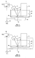
- FIG. 1 A laser beam 10 is reflected off a force-sensing cantilever 12 deflections of which are detected by a position sensitive detector 14.
- the cantilever is scanned over the sample surface 16 by a piezoelectric transducer 18.
- the force-sensing cantilever is immersed in a fluid body 20 contained in a fluid cell 22.
- the fluid cell 22 is mounted on a second transducer 24 which can displace the fluid cell 22 and sample surface 16 relative to the scanning transducer 18.
- An ac signal 26 is applied to the second transducer 24 so as to modulate the gap 28 between the force sensing probe tip 30 on cantilever 12 and the sample surface 16.
- the corresponding modulation of the laser beam position is detected by the detector 14.
- a synchronous detector 32 determines the amplitude and phase of the modulation. These signals are used to set the operating point of the microscope.
- the tip deflection is in phase with the modulation and the amplitude decreased by closer contact with the surface.
- the height of the tip is adjusted so as to give a constant, in phase, reduction of the modulation signal as the tip is scanned over the surface.
- a plot of these adjustments as a function of the position of the tip in the plane of the surface constitutes a topographical height map of the surface taken at constant interaction-force-gradient.
- Lindsay Neither do they describe a method for producing force-gradient images by using this technique to modulate the gap between the tip and sample.
- Lindsay has described a reproducible method for applying a force to a cantilever using an external magnetic field and also a method for forming images by modulating the position of the cantilever with this technique.
- the magnetic arrangement described by Lindsay requires either a large magnetic moment on the tip or a large field gradient.
- Florin et al Atomic force microscope with magnetic force modulation shows in Figure 1(b) thereof positioning a magnetic particle on the cantilever with the north-south poles being normal (perpendicular) to the long (soft) axis of the cantilever and using an external magnetic field to drive the tip.
- a particle of magnetic material is placed on the end of the cantilever with its magnetic moment M aligned along the direction of desired motion.
- a magnetic field gradient, dB/dz is applied along the same direction as the magnetic moment, resulting in a force F z along the Z direction
- F z M z (dB/dz)
- this method relies on the magnitude of dB/dz , but large magnetic field gradients are difficult to generate.
- US Patent No. 5,266,896 to Rugar et al differs from the present invention by teaching magnetizing the cantilever tip, not a magnetic particle or film on the back of the cantilever. Rugar et al does not teach how to magnetize only a cantilever tip nor what materials might be used. Nor does Rugar et al teach the specific method by which the tip is magnetized.
- Another object of the present invention is to use a method of modulation that is consistent with operation in fluids.
- Yet another object of the present invention is to produce force-sensing cantilevers that are consistently magnetized with a moment along the soft axis of the cantilever.
- a scanning probe microscope for generating a signal corresponding to the surface characteristics of a sample, said signal being for determining said characteristics
- said microscope comprising: a force sensing probe tip disposed on a first side of a free end of a flexible cantilever; a magnetic material disposed on a second side of said free end of said cantilever, said second side being opposite said first side; means for detecting bending of said cantilever and producing a deflection signal in response thereto; means for scanning said force sensing probe tip relative to the surface of the sample; an ac signal source; magnetic field generating means for generating a magnetic field, said magnetic field generating means responsive to said ac signal source for causing ac modulation of said magnetic field; and a synchronous detector responsive to said deflection signal and said ac signal for generating an output signal corresponding to surface characteristics of the scanned sample.
- the invention is characterized with respect to Florin et al in that said magnetic
- said magnetised material is a film, a particle or particles disposed on said second side of said cantilever.
- FIG. 3 shows the arrangement described in Lindsay, which is akin to that described in Florin et al and Lantz et al.
- a magnetic particle or film 33 is magnetized so that the resulting moment, M (34) lies perpendicular to the soft axis of the cantilever 36.
- M the resulting moment
- FIG. 4 A second arrangement, in accordance with the invention, is shown in FIG. 4.
- a film or particle 39 attached to the cantilever is magnetized with a moment M (40) along the soft axis of the cantilever 42.
- a magnetic field B (44) is applied normal to the soft axis of the cantilever.
- N M x B.
- a force F of magnitude F
- /R is applied to the end of the tip perpendicular to the soft axis of the cantilever.
- /R is applied to the end of the tip perpendicular to the soft axis of the cantilever.
- /R is applied to the end of the tip perpendicular to the soft axis of the cantilever.
- /R is applied to the end of the tip perpendicular to the soft axis of the cantilever.
- /R is applied to the end of the tip perpendicular to the soft axis of the cantilever.
- /R
- the inventive concept thus also embraces a method for magnetizing a thin film of magnetizable material disposed on a force sensing cantilever, comprising: placing the thin film of magnetizable material on the force sensing cantilever; placing the force sensing cantilever between two opposite poles of an electromagnet; and applying current to said electromagnet so as to generate a magnetic field between said opposite poles of said electromagnet while said force sensing cantilever is between said opposite poles.
- the invention is characterized with respect to Lantz et al in that a soft axis of said force sensing cantilever lies along the direction of said magnetic field so that the film, when magnetized, has a magnetic moment parallel to the soft axis.
- a thin film of a magnetic material is applied to one or both surfaces of a force sensing cantilever.
- the cantilevers are then placed between the poles of an electromagnet and a magnetizing field applied in the direction of the soft axis of the cantilevers.
- the field is chosen so as to be bigger than the saturation field for the magnetic film.
- a small electromagnet is placed in the housing of the microscope so as to generate a field normal to the soft axis of the cantilever.
- the field is generated by an ac voltage and causes a time varying force to be applied to the cantilever.
- the corresponding modulation of the cantilever position is sensed by reflection of a laser beam into a position sensitive detector.
- FIG. 1 is a schematic diagram of one prior art scheme for modulating the tip to substrate gap in force microscopy in fluids where the whole sample is moved up and down relative to the probe scanner.
- FIG. 2 is a schematic diagram of another prior art scheme where the modulating signal is applied directly to the probe scanner.
- FIG. 3 is a diagram of a prior art scheme for placing a magnetic force on a force-sensing cantilever.
- FIG. 4 is a diagram illustrating the arrangement used in the present invention: a field normal to the magnetic moment of the cantilever exerts a torque on the cantilever.
- FIG. 5 is a schematic diagram illustrating the overall layout of an ac magnetically modulated force sensing microscope constructed according to a presently preferred embodiment of the present invention.
- FIG. 6 is a schematic diagram illustrating the scheme used in the present invention for magnetizing the cantilevers and for calibrating the magnetization.
- FIG. 7 is a graphical plot illustrating a typical hysteresis loop for a magnetic thin film.
- FIG. 5 An overall layout of the scanning force microscope according to a presently preferred embodiment of the present invention is shown in FIG. 5.
- a thin film or particles of magnetic material 46 is applied to the back of a force-sensing cantilever 48 with the direction of the magnetic moment M along the soft axis of the cantilever 48.
- the cantilever 48 is attached to a scanning transducer 50 which holds it above the surface 52 of a sample 54 which may be submerged in a fluid body 56.
- a laser beam 58 is reflected from the back of the cantilever 48 into a position-sensitive detector 60 so that deflections of the cantilever 48 may be detected and recorded.
- a small solenoid 62 is placed near cantilever 48 so as to generate a magnetic field B that is predominantly perpendicular to the soft axis of cantilever 48.
- an alternating current (ac) voltage source 66 is used to drive the solenoid 62.
- the corresponding modulation level is detected by a synchronous detector 68 which is also driven with the ac signal 66 as a reference.
- the ac signal is preferably a sine wave. It is higher in frequency than the highest frequency associated with scanning a pixel, but generally equal to (or less than) the resonant frequency of the force sensing cantilever (which is typically about 50kHz).
- the synchronous detector averages that part of the input signal bearing a constant phase to the reference signal. If the input signal is S(t) and the reference signal (the signal that did the modulation) is A cos(wt), then the synchronous detector forms the averaged product: where f is a fixed phase shift (which can be set electronically to cancel systematic unwanted phase shifts or to detect the quadrature component of the signal) and t is a time constant for integration of the signal. This time constant is set equal to about the time taken to scan one pixel in the final image. In this way, the averaging does not loose resolution.
- the modulation period (2p/w) must be less than the integration time in order for averaging to occur.
- the microscope height (z height) is controlled by a feedback control loop as is well known to those of ordinary skill in the art.
- the output of the feedback control loop acts to adjust the output of the synchronous detector so that it remains constant while the z height is adjusted to achieve this.
- the topographical output of the microscope is the map of adjustments to the z height.
- the solenoid is made from several hundred turns of pile-wound wire 70 on a Permendur core 72 (available from Eagle Alloys of Jefferson City, Tennessee). This produces a field of about 100 Gauss at a distance of about 3mm from the pole piece when a current of 500mA is passed through the coil.
- An important step in the preparation of the cantilevers 48 is the formation of a controlled magnetic moment.
- One method for doing this is to place the cantilever in a strong magnetizing field.
- a film of Cobalt of about 500 angstroms thickness is evaporated onto the cantilever surface. Films of this thickness and composition are relatively easy to magnetize in the plane of the film.
- the magnetization can be monitored by simultaneous preparation of a film on a test substrate such as a wafer of silicon. This process is illustrated in FIG. 6.
- the cantilever 74 is coated with a magnetic film 76 and is placed between the pole pieces of an electromagnet 78, 80 with its soft axis lying along the field direction.
- Magnetization of the thin film 76 can be monitored using a separate test specimen, consisting of a silicon wafer 82 coated with an identical thin magnetic film 84.
- a laser beam 86 from an ellipsometer (not shown) is used to measure the local magnetization using rotation of the polarization of the incident light 86.
- the magnetic field is swept as the magnetization of the film is recorded.
- a typical magnetization curve for such a thin film is shown in FIG. 7. It shows the characteristic hysteresis loop due to the permanent magnetization of the sample at a saturation magnetization M s which occurs at a saturating field Hs.
- a typical value for M s is 1,400 emu/cm 3 and a typical value for H s is 400 Gauss.
- a force sensing cantilever has typical dimensions of 100 ⁇ m by 100 ⁇ m. Covered with a 500A thickness of cobalt film, this gives a volume of 5 x 10 -10 cm 3 of magnetic material. When magnetized to saturation, this yields a moment of 7 x 10 -10 emu. In a field of 100 Gauss normal to the magnetic moment, this results in a torque of 7 x 10 -5 dyne-cm. Thus, at the end of a 100 ⁇ m cantilever, the force is 7 x 10 -3 dyne or 7 x 10 -8 N. Thus, for a force-sensing cantilever with a spring constant of 0.1N/m, a reasonable magnetic field can move the tip by up to 100nm.
- the degree of control is adequate not only for applying modulation to the cantilever (where displacements of 0.01nm are adequate) but also for controlling instabilities in the cantilever position caused by attractive forces which pull the cantilever into the surface. This is described more fully in United States Patent Application Serial No. 08/246,035 (US-A-5 515 719 published 14, 5, 96).
Landscapes
- Physics & Mathematics (AREA)
- Health & Medical Sciences (AREA)
- General Health & Medical Sciences (AREA)
- General Physics & Mathematics (AREA)
- Nuclear Medicine, Radiotherapy & Molecular Imaging (AREA)
- Radiology & Medical Imaging (AREA)
- Engineering & Computer Science (AREA)
- Chemical & Material Sciences (AREA)
- Power Engineering (AREA)
- Nanotechnology (AREA)
- Analytical Chemistry (AREA)
- Crystallography & Structural Chemistry (AREA)
- Length Measuring Devices With Unspecified Measuring Means (AREA)
- A Measuring Device Byusing Mechanical Method (AREA)
- Measurement Of Length, Angles, Or The Like Using Electric Or Magnetic Means (AREA)
Claims (10)
- Fühler-Abtast-Mikroskop zur Generierung eines Signals entsprechend den Oberflächencharakteristiken einer Probe (54), wobei dieses Signal zur Bestimmung dieser Charakteristiken bestimmt ist und das Mikroskop mindestens umfaßt:dadurch gekennzeichnet, daßeinen Kräfte wahrnehmenden Fühlerkopf (64), der auf einer ersten Seite eines freien Endes eines flexiblen Auslegers (48) angeordnet ist,ein magnetisches Material (46), das auf einer zweiten Seite des freien Endes dieses Auslegers (48) angeordnet ist, wobei diese zweite Seite gegenüber der ersten Seite liegt,Mittel (60) für die Detektierung des Biegens dieses Auslegers (48) und für das Erzeugen eines Ausschlagsignals in Antwort dazu,Mittel (50) für das Abtasten dieses Kräfte wahrnehmenden Fühlerkopfes (64) relativ zur Oberfläche (52) der Probe (54),eine Wechselstrom-Signal-Quelle (66),Magnetfeld generierende Mittel (62) zur Generierung eines Magnetfeldes, wobei diese Magnetfeld generierenden Mittel (62) auf die Wechselstrom-Signal-Quelle (66) zur Erzeugung einer Wechselstrommodulation dieses Magnetfeldes ansprechen undeinem Synchrondetektor (68), der auf das Ausschlagsignal und das Wechselstromsignal zur Generierung eines Ausgangssignales entsprechend den Oberflächencharakteristiken der abgetasteten Probe (54) anspricht,
das Magnetfeld bei Gebrauch auf die zweite Seite des freien Endes des Auslegers (48) zu gerichtet ist und darum das magnetische Material (46) ein magnetisches Moment parallel zu der weichen Achse dieses flexiblen Auslegers (48) hat. - Fühler-Abtast-Mikroskop nach Anspruch 1, bei dem das magnetisierte Material (46) ein Film, ein Teilchen oder mehrere Teilchen, angeordnet auf der zweiten Seite des flexiblen Auslegers (48), ist.
- Fühler-Abtast-Mikroskop nach Anspruch 1, bei dem die das Magnetfeld generierenden Mittel eine Magnetspule (62) beinhalten.
- Fühler-Abtast-Mikroskop nach Anspruch 1, bei dem der flexible Ausleger (48), der Kräfte wahrnehmende Fühlerkopf (64) und die Probenoberfläche (52) in ein Fluid (56) eingetaucht sind.
- Fühler-Abtast-Mikroskop nach Anspruch 4, bei dem dieses Fluid (56) eine Flüssigkeit ist.
- Fühler-Abtast-Mikroskop nach Anspruch 5, bei dem dieses Fluid (56) Wasser ist.
- Verfahren zum Magnetisieren eines dünnen Films von magnetisierbarem Material (76), das auf einem Kräfte wahrnehmenden Ausleger (74) für ein Fühler-Abtast-Mikroskop angeordnet ist und umfaßt:dadurch gekennzeichnet, daßPlazieren des dünnen Films von magnetisierbarem Material (76) auf dem Kräfte wahrnehmenden Ausleger (74),Plazieren des Kräfte wahrnehmenden Auslegers (74) zwischen zwei entgegengesetzten Polen (78, 80) eines Elektromagneten, undAnlegen eines Stromes an diesen Elektromagneten, um ein Magnetfeld zwischen den entgegengesetzten Polen (78, 80) dieses Elektromagneten zu generieren, während der Kräfte wahrnehmende Ausleger (74) sich zwischen diesen entgegengesetzten Polen (78, 80) befindet,
eine weiche Achse des Kräfte wahrnehmenden Auslegers (74) entlang der Richtung des Magnetfeldes liegt, so daß der Film (76), sobald er magnetisiert ist, ein magnetisches Moment parallel zu der weichen Achse hat. - Verfahren nach Anspruch 7, das des weiteren umfaßt:Plazierung eines flachen Kalibrierungsobjektes (82) zwischen den entgegengesetzten Polen während des Verfahrensschrittes des Stromanlegens.
- Verfahren nach Anspruch 8, das des weiteren umfaßt:Benutzen eines Ellipsometers, um eine Messung der Magnetisierung dieses flachen Kalibrierungsobjektes (82) zu erhalten undBestimmung der Magnetisierung des Kräfte wahrnehmenden Auslegers (74) aufgrund dieser Messung.
- Verfahren nach Anspruch 7, das des weiteren umfaßt:Bildung eines flachen Kalibrierungsobjektes (82) aus einem nicht leitfähigen Material, undPlazierung eines dünnen Films von magnetisierbarem Material (84) auf diesen flachen Kalibrierungsobjekt (82), wobei dieser Film (84) aus dem gleichen Material ist wie der Film (76), der auf dem Kräfte wahrnehmenden Ausleger (74) plaziert ist und dieser Film (84) die gleiche Dicke hat wie der Film (76), der auf dem Kräfte wahrnehmenden Ausleger (74) plaziert ist und dieser Film (84) die gleiche Gesamtmasse hat wie der Film (76), der auf dem Kräfte wahrnehmenden Ausleger (74) plaziert ist.
Applications Claiming Priority (3)
| Application Number | Priority Date | Filing Date | Title |
|---|---|---|---|
| US403238 | 1995-03-10 | ||
| US08/403,238 US5513518A (en) | 1994-05-19 | 1995-03-10 | Magnetic modulation of force sensor for AC detection in an atomic force microscope |
| PCT/US1996/002753 WO1996028706A1 (en) | 1995-03-10 | 1996-02-29 | Magnetic modulation of force sensor for ac detection in an atomic force microscope |
Publications (3)
| Publication Number | Publication Date |
|---|---|
| EP0813675A1 EP0813675A1 (de) | 1997-12-29 |
| EP0813675A4 EP0813675A4 (de) | 1998-06-03 |
| EP0813675B1 true EP0813675B1 (de) | 2000-07-26 |
Family
ID=23595030
Family Applications (1)
| Application Number | Title | Priority Date | Filing Date |
|---|---|---|---|
| EP96910346A Expired - Lifetime EP0813675B1 (de) | 1995-03-10 | 1996-02-29 | Magnetische modulation des kraftsensors zur wechseldetektion in einem rasterkraftmikroskop |
Country Status (5)
| Country | Link |
|---|---|
| US (2) | US5513518A (de) |
| EP (1) | EP0813675B1 (de) |
| JP (1) | JP3249132B2 (de) |
| DE (1) | DE69609493T2 (de) |
| WO (1) | WO1996028706A1 (de) |
Families Citing this family (47)
| Publication number | Priority date | Publication date | Assignee | Title |
|---|---|---|---|---|
| US5983712A (en) * | 1994-05-19 | 1999-11-16 | Molecular Imaging Corporation | Microscope for compliance measurement |
| US5866805A (en) | 1994-05-19 | 1999-02-02 | Molecular Imaging Corporation Arizona Board Of Regents | Cantilevers for a magnetically driven atomic force microscope |
| US5753814A (en) | 1994-05-19 | 1998-05-19 | Molecular Imaging Corporation | Magnetically-oscillated probe microscope for operation in liquids |
| US5670712A (en) * | 1994-08-15 | 1997-09-23 | The Regents Of The University Of California | Method and apparatus for magnetic force control of a scanning probe |
| US5750989A (en) * | 1995-02-10 | 1998-05-12 | Molecular Imaging Corporation | Scanning probe microscope for use in fluids |
| US5621210A (en) * | 1995-02-10 | 1997-04-15 | Molecular Imaging Corporation | Microscope for force and tunneling microscopy in liquids |
| US5675154A (en) * | 1995-02-10 | 1997-10-07 | Molecular Imaging Corporation | Scanning probe microscope |
| EP0807799B1 (de) * | 1996-05-13 | 2002-10-09 | Seiko Instruments Inc. | Abtastgerät für eine Sonde |
| US6038916A (en) * | 1997-07-22 | 2000-03-21 | Digital Instruments | Method and apparatus for measuring energy dissipation by a probe during operation of an atomic force microscope |
| US6181131B1 (en) | 1997-07-25 | 2001-01-30 | University Of Washington | Magnetic resonance force microscopy with oscillator actuation |
| US6518570B1 (en) | 1998-04-03 | 2003-02-11 | Brookhaven Science Associates | Sensing mode atomic force microscope |
| US6121611A (en) * | 1998-05-20 | 2000-09-19 | Molecular Imaging Corporation | Force sensing probe for scanning probe microscopy |
| JP3235786B2 (ja) | 1998-06-30 | 2001-12-04 | 技術研究組合オングストロームテクノロジ研究機構 | 走査プローブの力制御方法 |
| US6330824B1 (en) | 1999-02-19 | 2001-12-18 | The University Of North Carolina At Chapel Hill | Photothermal modulation for oscillating mode atomic force microscopy in solution |
| DE10007617B4 (de) * | 1999-03-20 | 2006-04-20 | International Business Machines Corp. | Charakterisierung von Magnetfeldern |
| DE19912814C2 (de) | 1999-03-22 | 2002-02-14 | Max Planck Gesellschaft | Verfahren und Vorrichtung zur Rastertunnelmikroskopie |
| US6245204B1 (en) | 1999-03-23 | 2001-06-12 | Molecular Imaging Corporation | Vibrating tip conducting probe microscope |
| US6377066B1 (en) | 1999-07-09 | 2002-04-23 | Mfi Technologies Corporation | Method and apparatus for sub-micron imaging and probing on probe station |
| FR2807162B1 (fr) * | 2000-03-31 | 2002-06-28 | Inst Curie | Sonde d'analyse de surface pour un microscope a force atomique et microscope a force atomique la comportant |
| CN1483136A (zh) * | 2000-11-30 | 2004-03-17 | 阿赛勒姆研究股份有限公司 | 用于高精度位置测量的改进线性变量差接变压器 |
| SE0103781D0 (sv) * | 2001-11-12 | 2001-11-12 | Nanofactory Instruments Ab | Mätanordning för elektronmikroskop |
| US6668628B2 (en) | 2002-03-29 | 2003-12-30 | Xerox Corporation | Scanning probe system with spring probe |
| US6866255B2 (en) * | 2002-04-12 | 2005-03-15 | Xerox Corporation | Sputtered spring films with low stress anisotropy |
| ES2194607B1 (es) * | 2002-05-03 | 2005-03-16 | Consejo Superior Investigaciones Cientificas | Un dispositivo de control de una señal de excitacion de un elemento oscilador mecanico resonante, un dispositivo de medicion, un metodo para controlar la señal de excitacion, un metodo para realizar mediciones, un programa de ordenador y un dispositivo de almacenamiento. |
| US6952952B2 (en) * | 2002-11-01 | 2005-10-11 | Molecular Imaging Corporation | Topography and recognition imaging atomic force microscope and method of operation |
| US7191639B2 (en) * | 2003-04-08 | 2007-03-20 | California Institute Of Technology | On-chip magnetic force actuation of microcantilevers by coplanar coils |
| US7015584B2 (en) * | 2003-07-08 | 2006-03-21 | Xerox Corporation | High force metal plated spring structure |
| US6819125B1 (en) * | 2003-07-23 | 2004-11-16 | Micron Technology, Inc. | Method and apparatus for integrated circuit failure analysis |
| US20050088173A1 (en) * | 2003-10-24 | 2005-04-28 | Abraham David W. | Method and apparatus for tunable magnetic force interaction in a magnetic force microscope |
| KR100631208B1 (ko) | 2004-07-20 | 2006-10-04 | 삼성전자주식회사 | 전자기유도를 이용한 바이오결합 검출장치 및 이를 이용한검출 방법 |
| US7230440B2 (en) * | 2004-10-21 | 2007-06-12 | Palo Alto Research Center Incorporated | Curved spring structure with elongated section located under cantilevered section |
| US8330485B2 (en) * | 2004-10-21 | 2012-12-11 | Palo Alto Research Center Incorporated | Curved spring structure with downturned tip |
| US20070236213A1 (en) * | 2006-03-30 | 2007-10-11 | Paden Bradley E | Telemetry method and apparatus using magnetically-driven mems resonant structure |
| US8024963B2 (en) * | 2006-10-05 | 2011-09-27 | Asylum Research Corporation | Material property measurements using multiple frequency atomic force microscopy |
| ES2303491A1 (es) * | 2007-12-21 | 2008-08-01 | Universidad Politecnica De Madrid | Detector de campo magnetico, mecanico y miniaturizable y su funcionamiento. |
| WO2010044871A1 (en) | 2008-10-14 | 2010-04-22 | Roger Proksch | Integrated micro actuator and linear variable defferential transformer for high precision position measurements |
| US8955161B2 (en) | 2008-11-13 | 2015-02-10 | Bruker Nano, Inc. | Peakforce photothermal-based detection of IR nanoabsorption |
| KR101873936B1 (ko) * | 2008-11-13 | 2018-07-04 | 브루커 나노, 인코퍼레이션. | 탐침형 원자 현미경 |
| US8650660B2 (en) | 2008-11-13 | 2014-02-11 | Bruker Nano, Inc. | Method and apparatus of using peak force tapping mode to measure physical properties of a sample |
| US8484760B2 (en) | 2009-11-24 | 2013-07-09 | International Business Machines Corporation | Device comprising a cantilever and scanning system |
| MY156153A (en) | 2009-12-01 | 2016-01-15 | Bruker Nano Inc | Method and apparatus of operating a scanning probe microscope |
| US8726410B2 (en) * | 2010-07-30 | 2014-05-13 | The United States Of America As Represented By The Secretary Of The Air Force | Atomic force microscopy system and method for nanoscale measurement |
| CN102519354A (zh) * | 2011-11-18 | 2012-06-27 | 东南大学 | 扫描式触觉纹理检测装置 |
| US9395388B2 (en) | 2012-09-14 | 2016-07-19 | The University Of North Carolina At Chapel Hill | Methods, systems, and computer readable media for dual resonance frequency enhanced electrostatic force microscopy |
| CN104865408A (zh) * | 2015-04-28 | 2015-08-26 | 中山大学 | 一种调控原子力显微镜悬臂梁共振频率的方法和装置 |
| KR20190060769A (ko) | 2016-08-22 | 2019-06-03 | 브루커 나노, 아이엔씨. | 피크 포스 탭핑을 이용한 샘플의 적외선 특성 |
| CN110441559B (zh) * | 2019-08-26 | 2020-07-28 | 上海大学 | 一种力实时可调的微纳探针自动成型装置和控制方法 |
Family Cites Families (116)
| Publication number | Priority date | Publication date | Assignee | Title |
|---|---|---|---|---|
| GB1433887A (en) * | 1973-04-19 | 1976-03-17 | Bactomatic Inc | Microbiological detection apparatus |
| CH643397A5 (de) * | 1979-09-20 | 1984-05-30 | Ibm | Raster-tunnelmikroskop. |
| EP0071666B1 (de) * | 1981-08-10 | 1985-02-06 | International Business Machines Corporation | Elektrische bewegbare Träger |
| US4520570A (en) * | 1983-12-30 | 1985-06-04 | International Business Machines Corporation | Piezoelectric x-y-positioner |
| DE3572030D1 (en) * | 1985-03-07 | 1989-09-07 | Ibm | Scanning tunneling microscope |
| USRE33387E (en) * | 1985-11-26 | 1990-10-16 | International Business Machines Corporation | Atomic force microscope and method for imaging surfaces with atomic resolution |
| US4724318A (en) * | 1985-11-26 | 1988-02-09 | International Business Machines Corporation | Atomic force microscope and method for imaging surfaces with atomic resolution |
| DE3610540A1 (de) * | 1986-03-27 | 1987-10-01 | Kernforschungsanlage Juelich | Bewegungseinrichtung zur mikrobewegung von objekten |
| EP0252745A3 (de) * | 1986-07-11 | 1990-01-24 | AGENCY OF INDUSTRIAL SCIENCE & TECHNOLOGY MINISTRY OF INTERNATIONAL TRADE & INDUSTRY | Gerät zum Steuern relativer Verschiebungen |
| US4877957A (en) * | 1986-07-14 | 1989-10-31 | Olympus Optical Co., Ltd. | Scanning type tunnel microscope |
| EP0262253A1 (de) * | 1986-10-03 | 1988-04-06 | International Business Machines Corporation | Mikromechanische Fühlervorrichtung für atomare Kräfte |
| US4800274A (en) * | 1987-02-02 | 1989-01-24 | The Regents Of The University Of California | High resolution atomic force microscope |
| JPS643502A (en) * | 1987-06-25 | 1989-01-09 | Seiko Instr & Electronics | Scanning type tunnel microscope |
| EP0307211A3 (de) * | 1987-09-10 | 1991-05-15 | Seiko Instruments Inc. | Speicher-Lesegerät |
| US4868396A (en) * | 1987-10-13 | 1989-09-19 | Arizona Board Of Regents, Arizona State University | Cell and substrate for electrochemical STM studies |
| JP2566794B2 (ja) * | 1987-10-15 | 1996-12-25 | セイコー電子工業株式会社 | 走査型トンネル顕微鏡の測定方法 |
| US4823004A (en) * | 1987-11-24 | 1989-04-18 | California Institute Of Technology | Tunnel and field effect carrier ballistics |
| JPH06105262B2 (ja) * | 1987-11-27 | 1994-12-21 | セイコー電子工業株式会社 | 電気化学測定およびトンネル電流同時測定方法および装置 |
| DE68916667T2 (de) * | 1988-03-04 | 1995-01-12 | Kabushiki Kaisha Toshiba, Kawasaki, Kanagawa | Mikroskop. |
| US4956817A (en) * | 1988-05-26 | 1990-09-11 | Quanscan, Inc. | High density data storage and retrieval system |
| US5257024A (en) * | 1988-05-26 | 1993-10-26 | Quan-Scan, Inc. | Search position encoder |
| US4871938A (en) * | 1988-06-13 | 1989-10-03 | Digital Instruments, Inc. | Positioning device for a scanning tunneling microscope |
| DE3844659A1 (de) | 1988-07-03 | 1990-11-29 | Forschungszentrum Juelich Gmbh | Mikromanipulator |
| USRE34331E (en) * | 1988-07-06 | 1993-08-03 | Digital Instruments, Inc. | Feedback control for scanning tunnel microscopes |
| US4889988A (en) * | 1988-07-06 | 1989-12-26 | Digital Instruments, Inc. | Feedback control for scanning tunnel microscopes |
| US5009111A (en) * | 1988-08-31 | 1991-04-23 | Quanscan, Inc. | Differential force balance apparatus |
| US4999495A (en) * | 1988-08-31 | 1991-03-12 | Seiko Instruments Inc. | Scanning tunneling microscope |
| US5018865A (en) * | 1988-10-21 | 1991-05-28 | Ferrell Thomas L | Photon scanning tunneling microscopy |
| US4968390A (en) * | 1988-11-03 | 1990-11-06 | Board Of Regents, The University Of Texas System | High resolution deposition and etching in polymer films |
| US4947042A (en) * | 1988-12-13 | 1990-08-07 | Mitsubishi Denki Kabushiki Kaisha | Tunnel unit and scanning head for scanning tunneling microscope |
| JPH02187944A (ja) * | 1989-01-13 | 1990-07-24 | Sharp Corp | 再生装置 |
| JP2814256B2 (ja) * | 1989-01-31 | 1998-10-22 | セイコーインスツルメンツ株式会社 | 電気化学測定トンネル電流同時測定装置およびトンネル探針 |
| US4924091A (en) * | 1989-02-01 | 1990-05-08 | The Regents Of The University Of California | Scanning ion conductance microscope |
| US4935634A (en) * | 1989-03-13 | 1990-06-19 | The Regents Of The University Of California | Atomic force microscope with optional replaceable fluid cell |
| US4952857A (en) * | 1989-03-24 | 1990-08-28 | Quanscan, Inc. | Scanning micromechanical probe control system |
| US5260622A (en) * | 1989-03-24 | 1993-11-09 | Topometrix Corporation | High resolution electromechanical translation device |
| US4968914A (en) * | 1989-03-24 | 1990-11-06 | Quanscan, Inc. | High resolution electromechanical translation device |
| US5304924A (en) * | 1989-03-29 | 1994-04-19 | Canon Kabushiki Kaisha | Edge detector |
| US5260824A (en) * | 1989-04-24 | 1993-11-09 | Olympus Optical Co., Ltd. | Atomic force microscope |
| US5051646A (en) * | 1989-04-28 | 1991-09-24 | Digital Instruments, Inc. | Method of driving a piezoelectric scanner linearly with time |
| GB8910566D0 (en) * | 1989-05-08 | 1989-06-21 | Amersham Int Plc | Imaging apparatus and method |
| US5017010A (en) * | 1989-05-16 | 1991-05-21 | International Business Machines Corporation | High sensitivity position sensor and method |
| US5266801A (en) * | 1989-06-05 | 1993-11-30 | Digital Instruments, Inc. | Jumping probe microscope |
| US5229606A (en) * | 1989-06-05 | 1993-07-20 | Digital Instruments, Inc. | Jumping probe microscope |
| JP2909829B2 (ja) * | 1989-07-05 | 1999-06-23 | セイコーインスツルメンツ株式会社 | 位置合わせ機能付複合走査型トンネル顕微鏡 |
| JP2909828B2 (ja) * | 1989-07-05 | 1999-06-23 | セイコーインスツルメンツ株式会社 | 複合走査型トンネル顕微鏡 |
| US4992659A (en) * | 1989-07-27 | 1991-02-12 | International Business Machines Corporation | Near-field lorentz force microscopy |
| US4999494A (en) * | 1989-09-11 | 1991-03-12 | Digital Instruments, Inc. | System for scanning large sample areas with a scanning probe microscope |
| JP2815196B2 (ja) * | 1989-10-02 | 1998-10-27 | オリンパス光学工業株式会社 | 微細表面形状計測装置 |
| US5206702A (en) * | 1989-10-09 | 1993-04-27 | Olympus Optical Co., Ltd. | Technique for canceling the effect of external vibration on an atomic force microscope |
| US5003815A (en) * | 1989-10-20 | 1991-04-02 | International Business Machines Corporation | Atomic photo-absorption force microscope |
| US5025658A (en) * | 1989-11-28 | 1991-06-25 | Digital Instruments, Inc. | Compact atomic force microscope |
| US5189906A (en) * | 1989-11-28 | 1993-03-02 | Digital Instruments, Inc. | Compact atomic force microscope |
| US4954704A (en) * | 1989-12-04 | 1990-09-04 | Digital Instruments, Inc. | Method to increase the speed of a scanning probe microscope |
| US5224376A (en) * | 1989-12-08 | 1993-07-06 | Digital Instruments, Inc. | Atomic force microscope |
| US5237859A (en) * | 1989-12-08 | 1993-08-24 | Digital Instruments, Inc. | Atomic force microscope |
| US5202004A (en) * | 1989-12-20 | 1993-04-13 | Digital Instruments, Inc. | Scanning electrochemical microscopy |
| US4992728A (en) * | 1989-12-21 | 1991-02-12 | International Business Machines Corporation | Electrical probe incorporating scanning proximity microscope |
| US5289004A (en) * | 1990-03-27 | 1994-02-22 | Olympus Optical Co., Ltd. | Scanning probe microscope having cantilever and detecting sample characteristics by means of reflected sample examination light |
| US5066858A (en) * | 1990-04-18 | 1991-11-19 | Digital Instruments, Inc. | Scanning tunneling microscopes with correction for coupling effects |
| US5198715A (en) * | 1990-05-23 | 1993-03-30 | Digital Instruments, Inc. | Scanner for scanning probe microscopes having reduced Z-axis non-linearity |
| US5103095A (en) * | 1990-05-23 | 1992-04-07 | Digital Instruments, Inc. | Scanning probe microscope employing adjustable tilt and unitary head |
| US5253516A (en) * | 1990-05-23 | 1993-10-19 | Digital Instruments, Inc. | Atomic force microscope for small samples having dual-mode operating capability |
| US5245863A (en) * | 1990-07-11 | 1993-09-21 | Olympus Optical Co., Ltd. | Atomic probe microscope |
| US5077473A (en) * | 1990-07-26 | 1991-12-31 | Digital Instruments, Inc. | Drift compensation for scanning probe microscopes using an enhanced probe positioning system |
| US5081390A (en) * | 1990-08-13 | 1992-01-14 | Digital Instruments, Inc. | Method of operating a scanning probe microscope to improve drift characteristics |
| US5274230A (en) * | 1990-08-31 | 1993-12-28 | Olympus Optical Co., Ltd. | Scanning probe microscope having first and second optical waveguides |
| US5231286A (en) * | 1990-08-31 | 1993-07-27 | Olympus Optical Co., Ltd. | Scanning probe microscope utilizing an optical element in a waveguide for dividing the center part of the laser beam perpendicular to the waveguide |
| US5266897A (en) * | 1990-09-05 | 1993-11-30 | International Business Machines Corporation | Magnetic field observation with tunneling microscopy |
| JPH0758193B2 (ja) * | 1990-09-14 | 1995-06-21 | 三菱電機株式会社 | 原子間力顕微鏡の微動走査機構 |
| US5144833A (en) * | 1990-09-27 | 1992-09-08 | International Business Machines Corporation | Atomic force microscopy |
| JPH04161807A (ja) * | 1990-10-26 | 1992-06-05 | Olympus Optical Co Ltd | 走査型プローブ顕微鏡 |
| JP2915554B2 (ja) * | 1990-11-19 | 1999-07-05 | オリンパス光学工業株式会社 | バリアハイト測定装置 |
| JPH04188022A (ja) * | 1990-11-22 | 1992-07-06 | Olympus Optical Co Ltd | 変位検出装置 |
| US5283437A (en) * | 1990-12-21 | 1994-02-01 | International Business Machines Corporation | Pneumatically and electrostatically driven scanning tunneling microscope |
| US5107113A (en) * | 1990-12-26 | 1992-04-21 | Bell Communications Research, Inc. | Method and apparatus for correcting distortions in scanning tunneling microscope images |
| US5157251A (en) * | 1991-03-13 | 1992-10-20 | Park Scientific Instruments | Scanning force microscope having aligning and adjusting means |
| JP3000491B2 (ja) * | 1991-04-10 | 2000-01-17 | キヤノン株式会社 | カンチレバーユニット及びこれを用いた情報処理装置、原子間力顕微鏡、磁力顕微鏡 |
| US5293042A (en) * | 1991-05-10 | 1994-03-08 | Olympus Optical Co., Ltd. | Servo circuit of scanning probe microscope |
| JPH04337403A (ja) * | 1991-05-14 | 1992-11-25 | Olympus Optical Co Ltd | 光集積型変位センサー |
| JP2961334B2 (ja) * | 1991-05-28 | 1999-10-12 | セイコーインスツルメンツ株式会社 | 尖鋭な金属針を持つ原子間力顕微鏡のカンチレバー製造法 |
| US5319977A (en) | 1991-06-20 | 1994-06-14 | The Board Of Trustees Of The Leland Stanford Junior University | Near field acoustic ultrasonic microscope system and method |
| US5155361A (en) * | 1991-07-26 | 1992-10-13 | The Arizona Board Of Regents, A Body Corporate Acting For And On Behalf Of Arizona State University | Potentiostatic preparation of molecular adsorbates for scanning probe microscopy |
| JPH0540034A (ja) | 1991-08-08 | 1993-02-19 | Nikon Corp | 複合型顕微鏡 |
| US5317153A (en) * | 1991-08-08 | 1994-05-31 | Nikon Corporation | Scanning probe microscope |
| JPH0540009A (ja) * | 1991-08-08 | 1993-02-19 | Nikon Corp | 走査型トンネル顕微鏡 |
| US5323003A (en) | 1991-09-03 | 1994-06-21 | Canon Kabushiki Kaisha | Scanning probe microscope and method of observing sample by using such a microscope |
| US5210410A (en) * | 1991-09-26 | 1993-05-11 | The Board Of Trustees Of The Leland Stanford Junior University | Scanning probe microscope having scan correction |
| US5298975A (en) * | 1991-09-27 | 1994-03-29 | International Business Machines Corporation | Combined scanning force microscope and optical metrology tool |
| JP2598851B2 (ja) * | 1992-01-23 | 1997-04-09 | 松下電器産業株式会社 | 位置決め装置 |
| JP2501282B2 (ja) * | 1992-02-04 | 1996-05-29 | インターナショナル・ビジネス・マシーンズ・コーポレイション | 原子間力走査顕微鏡を使用した表面プロフィル検査方法及びその装置 |
| US5204531A (en) * | 1992-02-14 | 1993-04-20 | Digital Instruments, Inc. | Method of adjusting the size of the area scanned by a scanning probe |
| US5280341A (en) * | 1992-02-27 | 1994-01-18 | International Business Machines Corporation | Feedback controlled differential fiber interferometer |
| US5291775A (en) * | 1992-03-04 | 1994-03-08 | Topometrix | Scanning force microscope with integrated optics and cantilever mount |
| US5319960A (en) * | 1992-03-06 | 1994-06-14 | Topometrix | Scanning force microscope |
| JPH05256641A (ja) * | 1992-03-11 | 1993-10-05 | Olympus Optical Co Ltd | カンチレバー変位検出装置 |
| US5267471A (en) * | 1992-04-30 | 1993-12-07 | Ibm Corporation | Double cantilever sensor for atomic force microscope |
| JP3081979B2 (ja) | 1992-05-08 | 2000-08-28 | セイコーインスツルメンツ株式会社 | 顕微鏡 |
| US5266896A (en) * | 1992-06-09 | 1993-11-30 | International Business Machines Corporation | Mechanical detection and imaging of magnetic resonance by magnetic moment modulation |
| US5262643A (en) * | 1992-06-12 | 1993-11-16 | International Business Machines Corp. | Automatic tip approach method and apparatus for scanning probe microscope |
| JP3141555B2 (ja) * | 1992-08-10 | 2001-03-05 | 株式会社日立製作所 | 走査表面磁気顕微鏡 |
| US5306919A (en) * | 1992-09-21 | 1994-04-26 | Digital Instruments, Inc. | Positioning device for scanning probe microscopes |
| US5331589A (en) * | 1992-10-30 | 1994-07-19 | International Business Machines Corporation | Magnetic STM with a non-magnetic tip |
| US5314254A (en) * | 1992-11-03 | 1994-05-24 | Digital Instruments | Stiffness enhancer for movable stage assembly |
| US5308974B1 (en) * | 1992-11-30 | 1998-01-06 | Digital Instr Inc | Scanning probe microscope using stored data for vertical probe positioning |
| US5314829A (en) * | 1992-12-18 | 1994-05-24 | California Institute Of Technology | Method for imaging informational biological molecules on a semiconductor substrate |
| US5321977A (en) | 1992-12-31 | 1994-06-21 | International Business Machines Corporation | Integrated tip strain sensor for use in combination with a single axis atomic force microscope |
| US5338932A (en) | 1993-01-04 | 1994-08-16 | Motorola, Inc. | Method and apparatus for measuring the topography of a semiconductor device |
| US5307693A (en) * | 1993-01-21 | 1994-05-03 | At&T Bell Laboratories | Force-sensing system, including a magnetically mounted rocking element |
| JP2743761B2 (ja) | 1993-03-19 | 1998-04-22 | 松下電器産業株式会社 | 走査型プローブ顕微鏡および原子種同定方法 |
| US5461907A (en) | 1993-03-23 | 1995-10-31 | Regents Of The University Of California | Imaging, cutting, and collecting instrument and method |
| US5354985A (en) | 1993-06-03 | 1994-10-11 | Stanford University | Near field scanning optical and force microscope including cantilever and optical waveguide |
| US5388452A (en) * | 1993-10-15 | 1995-02-14 | Quesant Instrument Corporation | Detection system for atomic force microscopes |
| US5357105A (en) * | 1993-11-09 | 1994-10-18 | Quesant Instrument Corporation | Light modulated detection system for atomic force microscopes |
| US5515719A (en) * | 1994-05-19 | 1996-05-14 | Molecular Imaging Corporation | Controlled force microscope for operation in liquids |
| US5670712A (en) * | 1994-08-15 | 1997-09-23 | The Regents Of The University Of California | Method and apparatus for magnetic force control of a scanning probe |
-
1995
- 1995-03-10 US US08/403,238 patent/US5513518A/en not_active Expired - Lifetime
- 1995-11-07 US US08/553,111 patent/US5612491A/en not_active Expired - Lifetime
-
1996
- 1996-02-29 WO PCT/US1996/002753 patent/WO1996028706A1/en not_active Ceased
- 1996-02-29 JP JP52765996A patent/JP3249132B2/ja not_active Expired - Lifetime
- 1996-02-29 EP EP96910346A patent/EP0813675B1/de not_active Expired - Lifetime
- 1996-02-29 DE DE69609493T patent/DE69609493T2/de not_active Expired - Lifetime
Also Published As
| Publication number | Publication date |
|---|---|
| US5612491A (en) | 1997-03-18 |
| EP0813675A4 (de) | 1998-06-03 |
| JPH10511467A (ja) | 1998-11-04 |
| JP3249132B2 (ja) | 2002-01-21 |
| DE69609493T2 (de) | 2001-06-28 |
| EP0813675A1 (de) | 1997-12-29 |
| DE69609493D1 (de) | 2000-08-31 |
| US5513518A (en) | 1996-05-07 |
| WO1996028706A1 (en) | 1996-09-19 |
Similar Documents
| Publication | Publication Date | Title |
|---|---|---|
| US5513518A (en) | Magnetic modulation of force sensor for AC detection in an atomic force microscope | |
| US6134955A (en) | Magnetic modulation of force sensor for AC detection in an atomic force microscope | |
| US5925818A (en) | Method and apparatus for magnetic force control of a scanning probe | |
| US5515719A (en) | Controlled force microscope for operation in liquids | |
| US6121611A (en) | Force sensing probe for scanning probe microscopy | |
| US5918274A (en) | Detecting fields with a single-pass, dual-amplitude-mode scanning force microscope | |
| Martin et al. | High‐resolution magnetic imaging of domains in TbFe by force microscopy | |
| US10215773B2 (en) | Material property measurements using multiple frequency atomic force microscopy | |
| KR100961571B1 (ko) | 주사 탐침 현미경 | |
| US8448501B2 (en) | Multiple frequency atomic force microscopy | |
| EP1002216B1 (de) | Mikroskop zur nachgiebigkeitsmessung | |
| US6121771A (en) | Magnetic force microscopy probe with bar magnet tip | |
| Proksch et al. | Energy dissipation measurements in frequency-modulated scanning probe microscopy | |
| Zavala | Atomic force microscopy, a tool for characterization, synthesis and chemical processes | |
| US6448766B1 (en) | Method of imaging a magnetic field emanating from a surface using a conventional scanning force microscope | |
| Yamamoto et al. | Precise force curve detection system with a cantilever controlled by magnetic force feedback | |
| Yaminsky et al. | Magnetic force microscopy | |
| Valera et al. | A high performance magnetic force microscope | |
| WO2008156722A1 (en) | Material property measurements using multiple frequency atomic forece microsocopy | |
| JP3398411B2 (ja) | 磁気力顕微鏡 | |
| Foss et al. | Magnetic force microscopy for magneto-optic bit imaging | |
| Yamamoto et al. | Detection of Similar Elastic Properties Using a Magnetic Force Controlled Afm | |
| Liu | Magnetic dissipation force microscopy | |
| Dahlberg et al. | Microbes, magnetism, and microscopy | |
| JPH11142105A (ja) | フリクション・フォース・プローブ顕微鏡およびフリクション・フォース・プローブ顕微鏡を用いた原子種や材料の同定方法 |
Legal Events
| Date | Code | Title | Description |
|---|---|---|---|
| PUAI | Public reference made under article 153(3) epc to a published international application that has entered the european phase |
Free format text: ORIGINAL CODE: 0009012 |
|
| 17P | Request for examination filed |
Effective date: 19971006 |
|
| AK | Designated contracting states |
Kind code of ref document: A1 Designated state(s): CH DE FR GB LI |
|
| A4 | Supplementary search report drawn up and despatched |
Effective date: 19980409 |
|
| AK | Designated contracting states |
Kind code of ref document: A4 Designated state(s): CH DE FR GB LI |
|
| 17Q | First examination report despatched |
Effective date: 19980812 |
|
| GRAG | Despatch of communication of intention to grant |
Free format text: ORIGINAL CODE: EPIDOS AGRA |
|
| GRAG | Despatch of communication of intention to grant |
Free format text: ORIGINAL CODE: EPIDOS AGRA |
|
| GRAG | Despatch of communication of intention to grant |
Free format text: ORIGINAL CODE: EPIDOS AGRA |
|
| GRAH | Despatch of communication of intention to grant a patent |
Free format text: ORIGINAL CODE: EPIDOS IGRA |
|
| GRAH | Despatch of communication of intention to grant a patent |
Free format text: ORIGINAL CODE: EPIDOS IGRA |
|
| GRAA | (expected) grant |
Free format text: ORIGINAL CODE: 0009210 |
|
| AK | Designated contracting states |
Kind code of ref document: B1 Designated state(s): CH DE FR GB LI |
|
| REG | Reference to a national code |
Ref country code: CH Ref legal event code: EP |
|
| REF | Corresponds to: |
Ref document number: 69609493 Country of ref document: DE Date of ref document: 20000831 |
|
| ET | Fr: translation filed | ||
| REG | Reference to a national code |
Ref country code: CH Ref legal event code: NV Representative=s name: NOVAPAT INTERNATIONAL S.A. |
|
| RAP2 | Party data changed (patent owner data changed or rights of a patent transferred) |
Owner name: MOLECULAR IMAGING CORPORATION |
|
| PGFP | Annual fee paid to national office [announced via postgrant information from national office to epo] |
Ref country code: CH Payment date: 20010202 Year of fee payment: 6 |
|
| PLBE | No opposition filed within time limit |
Free format text: ORIGINAL CODE: 0009261 |
|
| STAA | Information on the status of an ep patent application or granted ep patent |
Free format text: STATUS: NO OPPOSITION FILED WITHIN TIME LIMIT |
|
| 26N | No opposition filed | ||
| REG | Reference to a national code |
Ref country code: GB Ref legal event code: IF02 |
|
| PG25 | Lapsed in a contracting state [announced via postgrant information from national office to epo] |
Ref country code: LI Free format text: LAPSE BECAUSE OF NON-PAYMENT OF DUE FEES Effective date: 20020228 Ref country code: CH Free format text: LAPSE BECAUSE OF NON-PAYMENT OF DUE FEES Effective date: 20020228 |
|
| REG | Reference to a national code |
Ref country code: CH Ref legal event code: PL |
|
| PGFP | Annual fee paid to national office [announced via postgrant information from national office to epo] |
Ref country code: FR Payment date: 20040219 Year of fee payment: 9 |
|
| PG25 | Lapsed in a contracting state [announced via postgrant information from national office to epo] |
Ref country code: FR Free format text: LAPSE BECAUSE OF NON-PAYMENT OF DUE FEES Effective date: 20051031 |
|
| REG | Reference to a national code |
Ref country code: FR Ref legal event code: ST Effective date: 20051031 |
|
| GBPC | Gb: european patent ceased through non-payment of renewal fee |
Effective date: 20070228 |
|
| PG25 | Lapsed in a contracting state [announced via postgrant information from national office to epo] |
Ref country code: GB Free format text: LAPSE BECAUSE OF NON-PAYMENT OF DUE FEES Effective date: 20070228 |
|
| PGFP | Annual fee paid to national office [announced via postgrant information from national office to epo] |
Ref country code: GB Payment date: 20060329 Year of fee payment: 11 |
|
| REG | Reference to a national code |
Ref country code: DE Ref legal event code: R082 Ref document number: 69609493 Country of ref document: DE Representative=s name: MEHLER ACHLER PATENTANWAELTE, DE |
|
| REG | Reference to a national code |
Ref country code: DE Ref legal event code: R082 Ref document number: 69609493 Country of ref document: DE Representative=s name: MEHLER ACHLER PATENTANWAELTE, DE |
|
| REG | Reference to a national code |
Ref country code: DE Ref legal event code: R082 Ref document number: 69609493 Country of ref document: DE Representative=s name: SCHOPPE, ZIMMERMANN, STOECKELER, ZINKLER, SCHE, DE Effective date: 20120121 Ref country code: DE Ref legal event code: R082 Ref document number: 69609493 Country of ref document: DE Representative=s name: SCHOPPE, ZIMMERMANN, STOECKELER, ZINKLER, SCHE, DE Effective date: 20120418 Ref country code: DE Ref legal event code: R082 Ref document number: 69609493 Country of ref document: DE Representative=s name: SCHOPPE, ZIMMERMANN, STOECKELER, ZINKLER & PAR, DE Effective date: 20120121 Ref country code: DE Ref legal event code: R082 Ref document number: 69609493 Country of ref document: DE Representative=s name: SCHOPPE, ZIMMERMANN, STOECKELER, ZINKLER & PAR, DE Effective date: 20120418 Ref country code: DE Ref legal event code: R081 Ref document number: 69609493 Country of ref document: DE Owner name: KEYSIGHT TECHNOLOGIES, INC., SANTA ROSA, US Free format text: FORMER OWNER: MOLECULAR IMAGING CORP., TEMPE, ARIZ., US Effective date: 20120418 Ref country code: DE Ref legal event code: R081 Ref document number: 69609493 Country of ref document: DE Owner name: AGILENT TECHNOLOGIES, INC. (N.D.GES.D. STAATES, US Free format text: FORMER OWNER: MOLECULAR IMAGING CORP., TEMPE, ARIZ., US Effective date: 20120418 Ref country code: DE Ref legal event code: R081 Ref document number: 69609493 Country of ref document: DE Owner name: AGILENT TECHNOLOGIES, INC. (N.D.GES.D. STAATES, US Free format text: FORMER OWNER: MOLECULAR IMAGING CORP., TEMPE, US Effective date: 20120418 |
|
| REG | Reference to a national code |
Ref country code: DE Ref legal event code: R082 Ref document number: 69609493 Country of ref document: DE Representative=s name: SCHOPPE, ZIMMERMANN, STOECKELER, ZINKLER, SCHE, DE Ref country code: DE Ref legal event code: R082 Ref document number: 69609493 Country of ref document: DE Representative=s name: SCHOPPE, ZIMMERMANN, STOECKELER, ZINKLER & PAR, DE |
|
| PGFP | Annual fee paid to national office [announced via postgrant information from national office to epo] |
Ref country code: DE Payment date: 20150224 Year of fee payment: 20 |
|
| REG | Reference to a national code |
Ref country code: DE Ref legal event code: R082 Ref document number: 69609493 Country of ref document: DE Representative=s name: SCHOPPE, ZIMMERMANN, STOECKELER, ZINKLER, SCHE, DE Ref country code: DE Ref legal event code: R081 Ref document number: 69609493 Country of ref document: DE Owner name: KEYSIGHT TECHNOLOGIES, INC., SANTA ROSA, US Free format text: FORMER OWNER: AGILENT TECHNOLOGIES, INC. (N.D.GES.D. STAATES DELAWARE), SANTA CLARA, CALIF., US |
|
| REG | Reference to a national code |
Ref country code: DE Ref legal event code: R071 Ref document number: 69609493 Country of ref document: DE |