EP0809290A2 - Mehrschicht-Verbindung für integrierte Schaltung - Google Patents
Mehrschicht-Verbindung für integrierte Schaltung Download PDFInfo
- Publication number
- EP0809290A2 EP0809290A2 EP97303230A EP97303230A EP0809290A2 EP 0809290 A2 EP0809290 A2 EP 0809290A2 EP 97303230 A EP97303230 A EP 97303230A EP 97303230 A EP97303230 A EP 97303230A EP 0809290 A2 EP0809290 A2 EP 0809290A2
- Authority
- EP
- European Patent Office
- Prior art keywords
- metal layer
- metal
- layer
- dielectric layer
- interconnect
- Prior art date
- Legal status (The legal status is an assumption and is not a legal conclusion. Google has not performed a legal analysis and makes no representation as to the accuracy of the status listed.)
- Withdrawn
Links
Images

Classifications
-
- H—ELECTRICITY
- H10—SEMICONDUCTOR DEVICES; ELECTRIC SOLID-STATE DEVICES NOT OTHERWISE PROVIDED FOR
- H10D—INORGANIC ELECTRIC SEMICONDUCTOR DEVICES
- H10D1/00—Resistors, capacitors or inductors
- H10D1/60—Capacitors
- H10D1/68—Capacitors having no potential barriers
-
- H10W20/01—
-
- H10W20/031—
-
- H10W20/496—
-
- H10W20/425—
-
- H10W20/4421—
-
- Y—GENERAL TAGGING OF NEW TECHNOLOGICAL DEVELOPMENTS; GENERAL TAGGING OF CROSS-SECTIONAL TECHNOLOGIES SPANNING OVER SEVERAL SECTIONS OF THE IPC; TECHNICAL SUBJECTS COVERED BY FORMER USPC CROSS-REFERENCE ART COLLECTIONS [XRACs] AND DIGESTS
- Y10—TECHNICAL SUBJECTS COVERED BY FORMER USPC
- Y10S—TECHNICAL SUBJECTS COVERED BY FORMER USPC CROSS-REFERENCE ART COLLECTIONS [XRACs] AND DIGESTS
- Y10S438/00—Semiconductor device manufacturing: process
- Y10S438/957—Making metal-insulator-metal device
Definitions
- the present invention relates to integrated circuit structures and fabrication and, more particularly, to the formation of interconnect wiring having improved resistance to electromigration and stress migration failure.
- connections referred to as interconnects
- interconnects While methods of depositing interconnection materials on wafers have become highly developed and can be performed with high manufacturing yield, connections, referred to as interconnects, formed at small sizes may fail after being put into service due to processes which occur within grains and grain boundaries of interconnect materials. Specifically, metal migration phenomena, known as electromigration and stress migration are principal causes of such failures. (The term “metal migration” is used hereinafter as generic to both stress migration failure and electromigration.)
- Electromigration is an incident of drift, motion, transport, migration, or displacement of metal atoms caused by passage of an electric current through an interconnect. Electromigration phenomena are affected by interconnect structure such as composition, grain size, layering and film orientation texture. For this reason, for example, large grain metal deposition is favoured for resistance of a single metal to electromigration. Metal migration causes an accumulation of metal atoms and a complementary formation of voids in the crystal lattice which may eventually lead to opening of the interconnect. The transport and piling-up of metal atoms may also cause the formation of so-called hillocks or extrusions which are localized increases in cross-sectional dimensions of the conductor. Such an increase in dimensions may cause an electrical short circuit to a nearby conductor or breakage of adjacent structures such as cracking of insulators which constitute another but related failure mode of a chip.
- Electromigration is enhanced at any point at which current density increases in a conductor such as at a notch, a void or a thinning of an interconnect. Electromigration thus tends to increase any irregularity in the formation of an interconnect and to accelerate over time.
- the principal mechanism of preventing electromigration has been to decrease current density in the electronic design of the integrated circuit which, of course, imposes a trade-off between circuit reliability and both performance (if current density is reduced by reduction of signal levels) and integration density (if current density is reduced by increased interconnect dimensions).
- Stress migration failure is also an incident of diffusion of metal atoms and is principally due to thermally induced stress. Specifically, while increase of temperature may tend to reduce stress in a semiconductor device, subsequent cooling increases stress while the device remains at a relatively high temperature allowing some relief of stress through material movement. A net migration of metal atoms can eventually cause opening of a conductor in the same manner as electromigration. Further, even when integrated circuits are carefully designed with cautious observance of current density levels in design and close tolerances in manufacture, the effects of stress-induced void formation can exacerbate electromigration effects.
- hafnium sandwich structure For example, a so-called hafnium sandwich structure is known and has shown particular promise by reducing electromigration and median time to failure, thereby increasing circuit reliability.
- a thin layer of hafnium is deposited on an aluminum layer and a further aluminum layer deposited thereover. Then, the aluminum and hafnium are reacted to form hafnium tri-aluminide (HfAl 3 ) at the interfaces.
- This structure provides a stable, dense barrier which prevents diffusion of aluminum between aluminum layers and the coincidence of voids or opens which might eventually develop.
- This structure does not prevent electromigration within each aluminum layer but an open or near-open which eventually develops in one aluminum layer would be able to heal before an open in the other aluminum alloy layer would be caused by an increase in current density at the same location in the other aluminum alloy layer.
- hafnium sandwich structure has additional unique problems and failure modes. Specifically, the formation of hafnium tri-aluminide is accompanied by a reduction of volume, causing void formation in the aluminum alloy. If the hafnium-aluminide is not completely formed prior to passivation, additional volume reduction may occur due to continuance of the reaction, further increasing stresses in surrounding structures and leading to defect formation. Formation of extrusions also occurs in the hafnium sandwich structure.
- topography As alluded to above, another failure mode of interconnections formed on integrated circuit chips is caused by severe topography over which a conductor is deposited. Further, severe topography can compromise the accuracy with which lithographic patterning can be carried out and may cause irregularity of conductor width and/or separation. Topography of sufficient severity to compromise conductor integrity may occur at any edge of any layer formed on the surface of the substrate or another layer such as a conductor crossing another conductor (and insulator) particularly if the layer is relatively thick or patterned in a manner to form a sharp angle with the surface of the substrate or other underlying layer, as may be required in many electronic elements.
- Trench capacitor structures employed to save space in, for example, large dynamic memories tend to exhibit variation in capacitance because of low carrier concentrations at interfaces of both capacitor plates.
- Another concern is the limited voltage which may be applied across the dielectric of a trench capacitor structure. While such a variation in capacitance and voltage limitation is generally tolerable in digital circuits, there are many types of analog circuits in which variation in capacitance with voltage is not tolerable and requires metal plates to increase carrier concentrations.
- the thickness of two metal plates and an intervening capacitor dielectric layer is generally sufficient to present severe topography and thus to compromise the integrity of conductors and other structures which may be formed thereover.
- an integrated circuit including an interconnect comprising portions of a first metal layer, a dielectric layer and a second metal layer, and further including a connection to both the first metal layer and the second metal layer of the interconnect.
- the same metal layers may be used to form the plates of a capacitor, a separate connection being provided in this case to each of the metal layers.
- the electrical connections in either case are formed as studs in an inter-level dielectric layer.
- a method of making an interconnect in an integrated circuit including the steps of depositing a first metal layer and a dielectric layer on a surface, patterning the first metal layer and the dielectric layer to form a first aperture, depositing a second metal layer on the dielectric layer, patterning the second metal layer to form a second aperture overlying the first aperture, and connecting the first metal layer and the second metal layer at an edge of the second aperture.
- the present invention thus provides both a metal conductor and metal-to-metal precision capacitor structure which are highly resistant to metal migration and can be formed with the same process.
- the method of the invention permits simultaneous production of interconnects which are highly resistant to metal migration coplanar with high precision capacitors.
- a semiconductor device structure in which a group of layers containing both interconnects and metal-to-metal capacitors also allows planarization of an overlying passivation layer or inter-level dielectric to be readily and economically achieved.
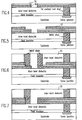
- Figure 1 there is shown, in cross-sectional view, an early stage in the fabrication of a semiconductor circuit structure in accordance with the invention.
- Figures 1 - 6 assume formation of the structure at a so-called first metal level for simplicity and to illustrate a useful form of plug or stud connection thereto but that the structure can also be formed directly on a substrate or on any layer of a multi-layer integrated circuit over a preferably planarized inter-level dielectric and preferably contiguous therewith.
- substrate 10 may have any number or type of integrated circuit structures formed thereon or therein, symbolically indicated by a junction 11 such as an implanted and/or diffused impurity conductive region 11 which may be connected to an overlying layer in a manner which will be described below.
- junction 11 such as an implanted and/or diffused impurity conductive region 11 which may be connected to an overlying layer in a manner which will be described below.
- Such structures as may be thus formed are then covered with a blanket field insulator 12, followed by an inter-level dielectric layer 13 which preferably can be planarized. Planarization can be accomplished by known techniques such as chemical-mechanical polishing. Layers 12 and 13 could also be formed by a single layer of insulating material.
- a connection is to be made to or from a lower layer (e.g. substrate 10)
- layers 12 and 13 are then patterned to form a via aperture for a plug or stud 14 of conductive material such as metal which is deposited therein.
- planarization can be delayed until after plug deposition or further planarization can be performed to remove metal from the upper surface of layer 13 and to avoid or limit protrusion of the metal plug above the upper surface of layer 13.
- a metal or alloy e.g. CuAlSi
- Each of the metal layers 15, 17 is preferably about one-half the nominal thickness of an interconnect in accordance with the design rules for a particular design. It is also considered preferable to form both metal layers of the same metal or alloy to obtain a consistent coefficient of thermal expansion. A thickness of about 150 nm is preferred and adequate to the practice of the invention. Thickness of insulator 16 is noncritical to the practice of the basic principles of the invention but should preferably be designed in view of a desired capacitance value and available capacitor plate area consistent with the electrical and physical integrity of the insulator material.
- the insulator material is similarly non-critical to the practice of the basic principles of the invention and silicon oxide, silicon nitride, and oxide-nitride-oxide layered structure or tantalum oxide may generally be used unless the capacitors of a particular circuit design requires a higher dielectric constant insulator, such as barium-strontium-titanate which can also be used in the practice of the invention.
- layers 15, 16 and 17 of the structure of Figure 1 are patterned to form capacitor plates (e.g. 21, 22) and a conductor (e.g. 23) and to form a stepped structure at a portion of each where connections are to be made.
- This patterning is preferably carried out in a two step process and the order of some steps is arbitrary or can be done as may be required by a particular design.
- portions of the layered structure comprising layers 15, 16 and 17 must be separated by etching down to the inter-level dielectric 13 to form the boundaries of the interconnect and/or capacitor structures and layer 17 must be etched to at least the dielectric layer 16 to form a stepped structure to facilitate connections thereto but in no particular order.
- dielectric layer 16 should be additionally patterned as desired interconnects may dictate. However, this can advantageously be done at the same time the inter-level dielectric 31 is patterned for formation of metal studs 32, 33 and 34, as will be described below with reference to Figure 3. If done separately however, it is generally preferable that the entire portion 16' exposed by opening of layer 17 should be removed for formation of connections to conductors and a lesser area 16'' should be removed for connection to capacitors to increase registration tolerances. However, removal of only a portion of the dielectric as shown at 16'' is adequate for the practice of the invention but may impose limits or a trade-off between registration tolerances and minimum stud size as will be evident to those skilled in the art in view of this description.
- the resist, exposure, resist development and etching methodology and process are completely arbitrary for practice of the basic principles of the invention although some processes and materials may be preferred for fabrication of particular designs, as will also be abundantly evident to those skilled in the art.
- a blanket inter-level dielectric 31 can be applied over and preferably contiguous with layer 17 and patterned by any technique suitable to the material thereof to form apertures where connections are to be made to metal layers 15 and 17 and via metal studs (e.g.32, 33 and 34) deposited, as described above.
- the deposition method for the metal studs is not important to the practice of the invention.
- the patterning of the inter-level dielectric 31, while not particularly critical as to accuracy or registration, is important to the formation of the structure in accordance with the invention since the connections made to layers 15, 17 determine the functions of those layers.
- metal studs 32, 33 are respectively connected to only one of layers 17, 15 since the structure at the right side of Figures 1 - 3 is intended to be a precision metal-to-metal capacitor. Stud 32 is connected to only the upper plate 22 and can be located at any point above the capacitor, just as stud 14 can be located at any point below the capacitor. The location of stud 33 is slightly more critical since it must contact only the lower capacitor plate 22 from above. However, the patterning (e.g. at 16'') of dielectric layer 16 provides a substantial region 35 upon which the location of stud 33 may encroach while correctly forming the connection. Similarly, the patterning of layer 15 provides a similar registration tolerance in the opposite direction.
- connection may be formed as illustrated between metal stud 14 and metal stud 33 through the capacitor plate 21 although either of studs 14 and 33 could be omitted as the design may require. If both connections are made, current density in the capacitor plate is generally not sufficiently great to cause metal migration since such a capacitor plate is generally at least several times the width of a conductor. However, since the connection is made only through metal layer 21, the relative location and proximity of studs 14 and 33 and current density limitation may be important design considerations.
- Metal stud 34 which corresponds to an interconnect termination (although one or more similar studs may be formed at intermediate locations along the length of the interconnect, as desired) contacts both layers 24 and 25 of the interconnect.
- registration tolerance is provided by the transverse dimension of metal stud 34 which can advantageously be enlarged somewhat relative to studs 32 and 33 and can be made comparable to registration tolerances 35 and 36.
- studs 32 and 33 are generally required to carry only currents sufficient to charge and discharge the precision metal-to-metal capacitor; which currents are generally small and of low duty cycle. Therefore, current carrying requirements of metal studs 32 and 33 are low and studs 32 and 33 can be made relatively small. Accordingly, it is preferable to size the transverse dimension of stud 34 in accordance with registration tolerance 36 and to form stud 33 as small as current carrying requirements permit in order to maximize registration tolerance 35. In any event, meeting registration tolerances can be readily achieved.
- the structure formed in accordance with the invention allows formation of a precision metal-to-metal capacitor in the same layer with an interconnect.
- Connection to the capacitor or conductor e.g. as shown by dashed lines 37
- the conductor which, in contrast to known redundant conductor structures has an insulator structure between the metal layers, is expected to be highly resistant to failure from electromigration and/or stress migration (particularly for aluminum) at least for the reason that thinning of one metal layer does not cause localized increase of current density in the other metal layer.
- Severe topography is avoided and the structure is readily and easily planarized to allow accurate lithography to form further layers having interconnects, capacitors and other electronic components therein. Additionally, process complexity and problems of corrosion and adhesion between layers associated with the use of diverse metals and alloys are avoided.
- this alternative method differs from that described above by patterning the metal and insulator layers 15 and 16 prior to formation of a following metal layer 17, as shown in Figure 4. Since this alternative process maintains a more nearly planar surface, lithographic exposure may be somewhat more accurately performed. This process may also be advantageously combined with other processes for forming other structures, depending on the chip design, since the metal deposition and patterning steps are separated.
- the dielectric layer 16 can serve to protect the surface of metal layer 15 from oxidation, corrosion and some additional processes which might be employed prior to deposition of metal layer 17.
- a second blanket metal layer 17 is deposited and patterned as shown in Figure 5. It should be noted that the patterning of layer 17 will also remove metal in the blanket layer which is deposited in the opening previously formed in layer 15. For this reason, it is preferable that the patterning be performed by an etching process which is highly selective between metal and dielectric layer 16 which can then serve as a mask for layer 15 to prevent further etching thereof during the process of patterning layer 17. The particular patterning process used is otherwise unimportant to the invention.
- the dielectric layer 16 can be further patterned either before or, preferably, after deposition of metal layer 17 but, as before, is advantageously patterned in accordance with patterning of the inter-level dielectric 31 for deposition of metal studs, as shown in Figure 6, to complete the structure.
- connection to both layers 15 and 17 can be made in a single material removal step. Particularly for aluminum, a substantially perpendicular end surface of the layered interconnect would then be formed. (Other combinations of metals and etch processes may form a sloping end face having some of the properties of both the embodiment of Figures 1 - 6 and Figure 7.)
- a metal stud can then be formed in an opening in inter-level dielectric 31 covering the end face of the interconnect and connected to both metal layers 15 and 17. Connections to the capacitor may be made with studs within the boundaries of the metal plates from respective sides of the layer.
- This embodiment of the invention is less preferred for most applications at the present time since the reduced contact area to the metal layers of the interconnect increases contact resistance. Potential contact area to the capacitor plates is unaffected but the embodiment is somewhat restricted in that connections to the capacitor plates cannot be made from the same side of the layer without additional structure which may negate space savings and reduction of process steps. However, chip space is saved for interconnects in comparison with a stepped structure and for capacitors in which the connections can be properly routed. Thus the embodiment of Figure 7 would be appropriate where integration density is of paramount importance. Further, as noted above, a patterning step would be saved relative to the variations of the invention illustrated in Figures 1 - 6 and the variation of Figure 7 may be relatively favoured for that reason.
- the invention provides a metal migration resistant interconnect in the same layer with a precision metal-to-metal capacitor.
- the interconnect and capacitor can be simultaneously formed in the same process with substantial increase in process economy and manufacturing yield.
- the structure can be formed at any desired level or any desired number of levels within an integrated circuit and planarization of an inter-level dielectric can be readily performed.
- the invention is expected to be most advantageously employed in integrated circuits, electronic devices of larger scale such as flexible chip carriers may advantageously employ the invention to concurrently form interconnects and capacitors in the same structural level even where metal migration is not observed.
- the invention provides an interconnect structure highly resistant to failure due to metal migration, even when aluminum and aluminum alloys are used which avoids problems of adhesion and corrosion incident to the use of dissimilar metals in a layered structure.
Landscapes
- Internal Circuitry In Semiconductor Integrated Circuit Devices (AREA)
- Semiconductor Integrated Circuits (AREA)
- Semiconductor Memories (AREA)
Applications Claiming Priority (2)
| Application Number | Priority Date | Filing Date | Title |
|---|---|---|---|
| US08/651,772 US5972788A (en) | 1996-05-22 | 1996-05-22 | Method of making flexible interconnections with dual-metal-dual-stud structure |
| US651772 | 1996-05-22 |
Publications (2)
| Publication Number | Publication Date |
|---|---|
| EP0809290A2 true EP0809290A2 (de) | 1997-11-26 |
| EP0809290A3 EP0809290A3 (de) | 2000-05-17 |
Family
ID=24614177
Family Applications (1)
| Application Number | Title | Priority Date | Filing Date |
|---|---|---|---|
| EP97303230A Withdrawn EP0809290A3 (de) | 1996-05-22 | 1997-05-12 | Mehrschicht-Verbindung für integrierte Schaltung |
Country Status (5)
| Country | Link |
|---|---|
| US (2) | US5972788A (de) |
| EP (1) | EP0809290A3 (de) |
| JP (1) | JP3197844B2 (de) |
| KR (1) | KR100252613B1 (de) |
| TW (1) | TW406389B (de) |
Cited By (1)
| Publication number | Priority date | Publication date | Assignee | Title |
|---|---|---|---|---|
| EP1143528A3 (de) * | 2000-02-02 | 2004-04-21 | Lsi Logic Corporation | In Verbindungsschicht eingebettete Metall-Isolator-Metall Kapazität und Verfahren zur Herstellung |
Families Citing this family (27)
| Publication number | Priority date | Publication date | Assignee | Title |
|---|---|---|---|---|
| US5985766A (en) * | 1997-02-27 | 1999-11-16 | Micron Technology, Inc. | Semiconductor processing methods of forming a contact opening |
| US6069398A (en) * | 1997-08-01 | 2000-05-30 | Advanced Micro Devices, Inc. | Thin film resistor and fabrication method thereof |
| US6245664B1 (en) * | 1998-01-05 | 2001-06-12 | Texas Instruments Incorporated | Method and system of interconnecting conductive elements in an integrated circuit |
| US6906370B1 (en) * | 1998-04-09 | 2005-06-14 | Infineon Technologies Ag | Semiconductor component having a material reinforced contact area |
| US6159787A (en) * | 1998-05-28 | 2000-12-12 | International Business Machines Corporation | Structures and processes for reduced topography trench capacitors |
| US6088258A (en) * | 1998-05-28 | 2000-07-11 | International Business Machines Corporation | Structures for reduced topography capacitors |
| EP0971403A1 (de) * | 1998-07-07 | 2000-01-12 | Interuniversitair Microelektronica Centrum Vzw | Herstellungsverfahren von Kupfer enthaltenden Metallstützen |
| US6972436B2 (en) * | 1998-08-28 | 2005-12-06 | Cree, Inc. | High voltage, high temperature capacitor and interconnection structures |
| KR20000012252U (ko) * | 1998-12-16 | 2000-07-05 | 전주범 | 압전소자를 사용한 커넥터 |
| US6497824B1 (en) * | 1999-09-23 | 2002-12-24 | Texas Instruments Incorporated | One mask solution for the integration of the thin film resistor |
| US6412786B1 (en) * | 1999-11-24 | 2002-07-02 | United Microelectronics Corp. | Die seal ring |
| JP4947849B2 (ja) * | 2001-05-30 | 2012-06-06 | ルネサスエレクトロニクス株式会社 | 半導体装置およびその製造方法 |
| JP2004022551A (ja) | 2002-06-12 | 2004-01-22 | Oki Electric Ind Co Ltd | 半導体素子の製造方法 |
| US6847077B2 (en) * | 2002-06-25 | 2005-01-25 | Agere Systems, Inc. | Capacitor for a semiconductor device and method for fabrication therefor |
| JP2006190889A (ja) * | 2005-01-07 | 2006-07-20 | Fujitsu Ltd | 半導体装置とその製造方法 |
| IL176056A (en) * | 2006-05-31 | 2012-02-29 | Avraham Shekalim | Drip irrigation system |
| WO2008010028A1 (en) * | 2006-06-15 | 2008-01-24 | Freescale Semiconductor, Inc. | Mim capacitor integration |
| JP5640438B2 (ja) * | 2010-04-15 | 2014-12-17 | 富士通セミコンダクター株式会社 | 半導体装置 |
| US8988895B2 (en) * | 2011-08-23 | 2015-03-24 | Tessera, Inc. | Interconnection elements with encased interconnects |
| US8941430B2 (en) * | 2012-09-12 | 2015-01-27 | Nvidia Corporation | Timing calibration for on-chip interconnect |
| US8689159B1 (en) * | 2012-09-12 | 2014-04-01 | Nvidia Corporation | Redundancy for on-chip interconnect |
| JP5925711B2 (ja) * | 2013-02-20 | 2016-05-25 | 浜松ホトニクス株式会社 | 検出器、pet装置及びx線ct装置 |
| US9305879B2 (en) | 2013-05-09 | 2016-04-05 | Globalfoundries Inc. | E-fuse with hybrid metallization |
| US9536830B2 (en) | 2013-05-09 | 2017-01-03 | Globalfoundries Inc. | High performance refractory metal / copper interconnects to eliminate electromigration |
| US9059166B2 (en) | 2013-05-09 | 2015-06-16 | International Business Machines Corporation | Interconnect with hybrid metallization |
| US9171801B2 (en) | 2013-05-09 | 2015-10-27 | Globalfoundries U.S. 2 Llc | E-fuse with hybrid metallization |
| US11600519B2 (en) * | 2019-09-16 | 2023-03-07 | International Business Machines Corporation | Skip-via proximity interconnect |
Family Cites Families (24)
| Publication number | Priority date | Publication date | Assignee | Title |
|---|---|---|---|---|
| FR2526225B1 (fr) * | 1982-04-30 | 1985-11-08 | Radiotechnique Compelec | Procede de realisation d'un condensateur integre, et dispositif ainsi obtenu |
| US4553050A (en) * | 1983-12-27 | 1985-11-12 | International Business Machines Corporation | Transmission line terminator-decoupling capacitor chip for off-chip driver |
| JPS60257553A (ja) * | 1984-06-04 | 1985-12-19 | Oki Electric Ind Co Ltd | 半導体装置 |
| US4767724A (en) * | 1986-03-27 | 1988-08-30 | General Electric Company | Unframed via interconnection with dielectric etch stop |
| US4920072A (en) * | 1988-10-31 | 1990-04-24 | Texas Instruments Incorporated | Method of forming metal interconnects |
| US4962058A (en) * | 1989-04-14 | 1990-10-09 | International Business Machines Corporation | Process for fabricating multi-level integrated circuit wiring structure from a single metal deposit |
| JPH03142973A (ja) * | 1989-10-30 | 1991-06-18 | Seiko Epson Corp | 半導体記憶装置 |
| JP3469251B2 (ja) * | 1990-02-14 | 2003-11-25 | 株式会社東芝 | 半導体装置の製造方法 |
| EP0469214A1 (de) * | 1990-07-31 | 1992-02-05 | International Business Machines Corporation | Verfahren zur Herstellung geschichteter Leiter- und/oder Widerstandsbereiche in Multiebenen-Halbleiterbauelementen und daraus resultierende Struktur |
| US5290396A (en) * | 1991-06-06 | 1994-03-01 | Lsi Logic Corporation | Trench planarization techniques |
| US5406447A (en) * | 1992-01-06 | 1995-04-11 | Nec Corporation | Capacitor used in an integrated circuit and comprising opposing electrodes having barrier metal films in contact with a dielectric film |
| JPH06125013A (ja) * | 1992-03-14 | 1994-05-06 | Toshiba Corp | 半導体装置及びその製造方法 |
| DE69333864T2 (de) * | 1992-06-12 | 2006-06-29 | Matsushita Electric Industrial Co., Ltd., Kadoma | Herstellungsverfahren für Halbleiterbauelement mit Kondensator |
| KR0136684B1 (en) * | 1993-06-01 | 1998-04-29 | Matsushita Electric Industrial Co Ltd | Semiconductor device and manufacture thereof |
| JPH0738068A (ja) * | 1993-06-28 | 1995-02-07 | Mitsubishi Electric Corp | 半導体装置およびその製造方法 |
| US5444022A (en) * | 1993-12-29 | 1995-08-22 | Intel Corporation | Method of fabricating an interconnection structure for an integrated circuit |
| US5366911A (en) * | 1994-05-11 | 1994-11-22 | United Microelectronics Corporation | VLSI process with global planarization |
| KR0138305B1 (ko) * | 1994-11-30 | 1998-06-01 | 김광호 | 반도체소자 배선형성방법 |
| JPH08181282A (ja) * | 1994-12-21 | 1996-07-12 | Sony Corp | 半導体装置製造方法 |
| US5534462A (en) * | 1995-02-24 | 1996-07-09 | Motorola, Inc. | Method for forming a plug and semiconductor device having the same |
| US5593919A (en) * | 1995-09-05 | 1997-01-14 | Motorola Inc. | Process for forming a semiconductor device including conductive members |
| JP2755243B2 (ja) * | 1996-01-23 | 1998-05-20 | 日本電気株式会社 | 半導体記憶装置およびその製造方法 |
| US5741626A (en) * | 1996-04-15 | 1998-04-21 | Motorola, Inc. | Method for forming a dielectric tantalum nitride layer as an anti-reflective coating (ARC) |
| US5874770A (en) * | 1996-10-10 | 1999-02-23 | General Electric Company | Flexible interconnect film including resistor and capacitor layers |
-
1996
- 1996-05-22 US US08/651,772 patent/US5972788A/en not_active Expired - Fee Related
- 1996-12-06 TW TW085115115A patent/TW406389B/zh not_active IP Right Cessation
-
1997
- 1997-03-25 KR KR1019970010305A patent/KR100252613B1/ko not_active Expired - Fee Related
- 1997-05-12 EP EP97303230A patent/EP0809290A3/de not_active Withdrawn
- 1997-05-12 JP JP12113097A patent/JP3197844B2/ja not_active Expired - Fee Related
-
1999
- 1999-07-12 US US09/351,440 patent/US6426544B1/en not_active Expired - Fee Related
Cited By (1)
| Publication number | Priority date | Publication date | Assignee | Title |
|---|---|---|---|---|
| EP1143528A3 (de) * | 2000-02-02 | 2004-04-21 | Lsi Logic Corporation | In Verbindungsschicht eingebettete Metall-Isolator-Metall Kapazität und Verfahren zur Herstellung |
Also Published As
| Publication number | Publication date |
|---|---|
| US20020053716A1 (en) | 2002-05-09 |
| US6426544B1 (en) | 2002-07-30 |
| TW406389B (en) | 2000-09-21 |
| US5972788A (en) | 1999-10-26 |
| JP3197844B2 (ja) | 2001-08-13 |
| JPH1056063A (ja) | 1998-02-24 |
| KR100252613B1 (ko) | 2000-04-15 |
| KR970077352A (ko) | 1997-12-12 |
| EP0809290A3 (de) | 2000-05-17 |
Similar Documents
| Publication | Publication Date | Title |
|---|---|---|
| US5972788A (en) | Method of making flexible interconnections with dual-metal-dual-stud structure | |
| US5541442A (en) | Integrated compact capacitor-resistor/inductor configuration | |
| EP0176010B1 (de) | Herstellungsverfahren für integrierte Schaltungen und Anordnung | |
| EP0129476B1 (de) | Planare verkettete Schaltung für integrierte Schaltkreise | |
| US6847077B2 (en) | Capacitor for a semiconductor device and method for fabrication therefor | |
| US6025275A (en) | Method of forming improved thick plated copper interconnect and associated auxiliary metal interconnect | |
| US6309958B1 (en) | Semiconductor device and method of manufacturing the same | |
| EP0908945A2 (de) | Doppel Damaszene mit selbstjustierten Durchkontaktierungen | |
| US5759912A (en) | Method of manufacturing a semiconductor device having multi-layered wiring without hillocks at the insulating layers | |
| US6790780B2 (en) | Fabrication of 3-D capacitor with dual damascene process | |
| KR100233315B1 (ko) | 반도체 집적 회로 및 그 제조 방법 | |
| US6200890B1 (en) | Method of fabricating copper damascene | |
| US6445071B1 (en) | Semiconductor device having an improved multi-layer interconnection structure and manufacturing method thereof | |
| JPH10229086A (ja) | 半導体装置およびその製造方法 | |
| KR100257481B1 (ko) | 플러그 금속막을 구비한 반도체 소자의 금속배선 형성방법 | |
| US6472697B2 (en) | Assorted aluminum wiring design to enhance chip-level performance for deep sub-micron application | |
| JPH05226475A (ja) | 半導体装置の製造方法 | |
| KR960014462B1 (ko) | 다층 금속배선 형성 방법 | |
| KR100230731B1 (ko) | 반도체 디바이스의 콘택 구조 및 그 제조방법 | |
| JP4089316B2 (ja) | 半導体装置およびその製造方法 | |
| KR100191710B1 (ko) | 반도체 소자의 금속 배선 방법 | |
| JPH11186386A (ja) | 半導体装置およびその製造方法 | |
| KR20000026376A (ko) | 다층 배선 형성을 위한 다마신 방법 | |
| JPH0786209A (ja) | 半導体装置の製造方法 | |
| JP2738358B2 (ja) | 半導体装置の製造方法 |
Legal Events
| Date | Code | Title | Description |
|---|---|---|---|
| PUAI | Public reference made under article 153(3) epc to a published international application that has entered the european phase |
Free format text: ORIGINAL CODE: 0009012 |
|
| AK | Designated contracting states |
Kind code of ref document: A2 Designated state(s): DE FR GB |
|
| PUAL | Search report despatched |
Free format text: ORIGINAL CODE: 0009013 |
|
| AK | Designated contracting states |
Kind code of ref document: A3 Designated state(s): DE FR GB |
|
| 17P | Request for examination filed |
Effective date: 20001025 |
|
| 17Q | First examination report despatched |
Effective date: 20040525 |
|
| STAA | Information on the status of an ep patent application or granted ep patent |
Free format text: STATUS: THE APPLICATION IS DEEMED TO BE WITHDRAWN |
|
| 18D | Application deemed to be withdrawn |
Effective date: 20041005 |