EP0803897A2 - Elektrode für Plasmaätzen - Google Patents
Elektrode für Plasmaätzen Download PDFInfo
- Publication number
- EP0803897A2 EP0803897A2 EP97302745A EP97302745A EP0803897A2 EP 0803897 A2 EP0803897 A2 EP 0803897A2 EP 97302745 A EP97302745 A EP 97302745A EP 97302745 A EP97302745 A EP 97302745A EP 0803897 A2 EP0803897 A2 EP 0803897A2
- Authority
- EP
- European Patent Office
- Prior art keywords
- electrode
- carbon material
- plasma
- glassy carbon
- plasma etching
- Prior art date
- Legal status (The legal status is an assumption and is not a legal conclusion. Google has not performed a legal analysis and makes no representation as to the accuracy of the status listed.)
- Granted
Links
- 238000001020 plasma etching Methods 0.000 title claims abstract description 24
- 239000003575 carbonaceous material Substances 0.000 claims abstract description 45
- 229910021397 glassy carbon Inorganic materials 0.000 claims abstract description 34
- 229910052710 silicon Inorganic materials 0.000 claims abstract description 18
- 239000010703 silicon Substances 0.000 claims abstract description 18
- 229910052751 metal Inorganic materials 0.000 claims abstract description 13
- 239000002184 metal Substances 0.000 claims abstract description 13
- 239000000428 dust Substances 0.000 abstract description 5
- XUIMIQQOPSSXEZ-UHFFFAOYSA-N Silicon Chemical compound [Si] XUIMIQQOPSSXEZ-UHFFFAOYSA-N 0.000 description 16
- 239000000463 material Substances 0.000 description 9
- OKTJSMMVPCPJKN-UHFFFAOYSA-N Carbon Chemical compound [C] OKTJSMMVPCPJKN-UHFFFAOYSA-N 0.000 description 7
- 238000000034 method Methods 0.000 description 7
- 239000011347 resin Substances 0.000 description 7
- 229920005989 resin Polymers 0.000 description 7
- XPFVYQJUAUNWIW-UHFFFAOYSA-N furfuryl alcohol Chemical compound OCC1=CC=CO1 XPFVYQJUAUNWIW-UHFFFAOYSA-N 0.000 description 6
- 229910002804 graphite Inorganic materials 0.000 description 6
- 239000010439 graphite Substances 0.000 description 6
- 238000003754 machining Methods 0.000 description 6
- 238000005530 etching Methods 0.000 description 5
- 239000002245 particle Substances 0.000 description 5
- CSCPPACGZOOCGX-UHFFFAOYSA-N Acetone Chemical compound CC(C)=O CSCPPACGZOOCGX-UHFFFAOYSA-N 0.000 description 4
- 230000000052 comparative effect Effects 0.000 description 4
- 239000004065 semiconductor Substances 0.000 description 4
- 239000000853 adhesive Substances 0.000 description 3
- 230000001070 adhesive effect Effects 0.000 description 3
- 238000005219 brazing Methods 0.000 description 3
- 238000005470 impregnation Methods 0.000 description 3
- XKRFYHLGVUSROY-UHFFFAOYSA-N Argon Chemical compound [Ar] XKRFYHLGVUSROY-UHFFFAOYSA-N 0.000 description 2
- XPDWGBQVDMORPB-UHFFFAOYSA-N Fluoroform Chemical compound FC(F)F XPDWGBQVDMORPB-UHFFFAOYSA-N 0.000 description 2
- 239000001913 cellulose Substances 0.000 description 2
- 229920002678 cellulose Polymers 0.000 description 2
- 239000011248 coating agent Substances 0.000 description 2
- 238000000576 coating method Methods 0.000 description 2
- 238000005553 drilling Methods 0.000 description 2
- 239000000945 filler Substances 0.000 description 2
- 239000007849 furan resin Substances 0.000 description 2
- 229920005546 furfural resin Polymers 0.000 description 2
- 238000004519 manufacturing process Methods 0.000 description 2
- 239000000203 mixture Substances 0.000 description 2
- 239000005011 phenolic resin Substances 0.000 description 2
- 238000005498 polishing Methods 0.000 description 2
- 239000012495 reaction gas Substances 0.000 description 2
- 238000005507 spraying Methods 0.000 description 2
- 230000003746 surface roughness Effects 0.000 description 2
- 229920001187 thermosetting polymer Polymers 0.000 description 2
- ZOXJGFHDIHLPTG-UHFFFAOYSA-N Boron Chemical compound [B] ZOXJGFHDIHLPTG-UHFFFAOYSA-N 0.000 description 1
- 239000003082 abrasive agent Substances 0.000 description 1
- 238000004026 adhesive bonding Methods 0.000 description 1
- 229910052782 aluminium Inorganic materials 0.000 description 1
- XAGFODPZIPBFFR-UHFFFAOYSA-N aluminium Chemical compound [Al] XAGFODPZIPBFFR-UHFFFAOYSA-N 0.000 description 1
- 229910052786 argon Inorganic materials 0.000 description 1
- QVGXLLKOCUKJST-UHFFFAOYSA-N atomic oxygen Chemical compound [O] QVGXLLKOCUKJST-UHFFFAOYSA-N 0.000 description 1
- 229910052796 boron Inorganic materials 0.000 description 1
- 229910052799 carbon Inorganic materials 0.000 description 1
- 238000004891 communication Methods 0.000 description 1
- 239000013078 crystal Substances 0.000 description 1
- 230000000694 effects Effects 0.000 description 1
- 230000001747 exhibiting effect Effects 0.000 description 1
- -1 for example Substances 0.000 description 1
- 239000007789 gas Substances 0.000 description 1
- 239000012535 impurity Substances 0.000 description 1
- 229910052738 indium Inorganic materials 0.000 description 1
- APFVFJFRJDLVQX-UHFFFAOYSA-N indium atom Chemical compound [In] APFVFJFRJDLVQX-UHFFFAOYSA-N 0.000 description 1
- 230000010354 integration Effects 0.000 description 1
- 238000005304 joining Methods 0.000 description 1
- 229910021421 monocrystalline silicon Inorganic materials 0.000 description 1
- 230000003287 optical effect Effects 0.000 description 1
- 239000001301 oxygen Substances 0.000 description 1
- 229910052760 oxygen Inorganic materials 0.000 description 1
- 238000005268 plasma chemical vapour deposition Methods 0.000 description 1
- 239000010453 quartz Substances 0.000 description 1
- VYPSYNLAJGMNEJ-UHFFFAOYSA-N silicon dioxide Inorganic materials O=[Si]=O VYPSYNLAJGMNEJ-UHFFFAOYSA-N 0.000 description 1
- 239000002904 solvent Substances 0.000 description 1
- 238000004544 sputter deposition Methods 0.000 description 1
- XLYOFNOQVPJJNP-UHFFFAOYSA-N water Substances O XLYOFNOQVPJJNP-UHFFFAOYSA-N 0.000 description 1
Images


Classifications
-
- C—CHEMISTRY; METALLURGY
- C23—COATING METALLIC MATERIAL; COATING MATERIAL WITH METALLIC MATERIAL; CHEMICAL SURFACE TREATMENT; DIFFUSION TREATMENT OF METALLIC MATERIAL; COATING BY VACUUM EVAPORATION, BY SPUTTERING, BY ION IMPLANTATION OR BY CHEMICAL VAPOUR DEPOSITION, IN GENERAL; INHIBITING CORROSION OF METALLIC MATERIAL OR INCRUSTATION IN GENERAL
- C23F—NON-MECHANICAL REMOVAL OF METALLIC MATERIAL FROM SURFACE; INHIBITING CORROSION OF METALLIC MATERIAL OR INCRUSTATION IN GENERAL; MULTI-STEP PROCESSES FOR SURFACE TREATMENT OF METALLIC MATERIAL INVOLVING AT LEAST ONE PROCESS PROVIDED FOR IN CLASS C23 AND AT LEAST ONE PROCESS COVERED BY SUBCLASS C21D OR C22F OR CLASS C25
- C23F4/00—Processes for removing metallic material from surfaces, not provided for in group C23F1/00 or C23F3/00
-
- H—ELECTRICITY
- H01—ELECTRIC ELEMENTS
- H01J—ELECTRIC DISCHARGE TUBES OR DISCHARGE LAMPS
- H01J37/00—Discharge tubes with provision for introducing objects or material to be exposed to the discharge, e.g. for the purpose of examination or processing thereof
- H01J37/32—Gas-filled discharge tubes
- H01J37/32431—Constructional details of the reactor
- H01J37/32532—Electrodes
- H01J37/32559—Protection means, e.g. coatings
-
- Y—GENERAL TAGGING OF NEW TECHNOLOGICAL DEVELOPMENTS; GENERAL TAGGING OF CROSS-SECTIONAL TECHNOLOGIES SPANNING OVER SEVERAL SECTIONS OF THE IPC; TECHNICAL SUBJECTS COVERED BY FORMER USPC CROSS-REFERENCE ART COLLECTIONS [XRACs] AND DIGESTS
- Y10—TECHNICAL SUBJECTS COVERED BY FORMER USPC
- Y10S—TECHNICAL SUBJECTS COVERED BY FORMER USPC CROSS-REFERENCE ART COLLECTIONS [XRACs] AND DIGESTS
- Y10S156/00—Adhesive bonding and miscellaneous chemical manufacture
- Y10S156/914—Differential etching apparatus including particular materials of construction
Definitions
- the present invention relates to an electrode for plasma etching, e.g. as used for production of semiconductor integrated circuits, such as LSIs or ICs, or waveguides for optical communication.
- Electrodes formed of aluminum, graphite, glassy carbon, metal silicon, quartz, and the like have been used particularly for production of semiconductors with finer-geometries and higher integration.
- the electrodes formed of metal silicon and glassy carbon are expensive, and therefore, it has been required to develop an inexpensive electrode in place of such expensive electrodes.
- Preferred embodiments of the present invention may provide an electrode for plasma etching, which is reduced in cost while keeping a high electrode performance.
- the present inventor has earnestly studied to achieve the above object, and found that an electrode for plasma etching, which is reduced in cost while enabling high accurate etching, can be obtained by a method wherein a portion to be consumed by plasma is formed of metal silicon or a glassy carbon material and the remaining portion is formed of a carbon material covered with a film of a glassy carbon material.
- an etching electrode In an etching electrode, although its shape is varied depending on the application, a portion to be actually consumed and to directly exert an effect on etching characteristics by, for example, generation of dust is a portion being in contact with plasma.
- the remaining portion such as an electrode mounting portion is also formed of an expensive single material such as metal silicon or a glassy carbon material.
- Such an etching electrode is replaced when only part of the surface of the electrode is consumed, and the spent electrode is discarded. In other words, the entire expensive material is discard after only part thereof is consumed, which leads to the increased running cost of plasma etching using such an electrode, resulting in the increased cost of semiconductors processed by the plasma etching.
- a portion of an electrode to be consumed by plasma is formed of metal silicon or a glassy carbon material just as in the conventional electrode and the remaining portion is formed of an inexpensive material having a conductivity required for the electrode, and from this viewpoint, an examination has been made by the present inventor to use a carbon material, for example, graphite as a material forming a portion other than a portion to be consumed by plasma.
- a carbon material for example, graphite
- the present inventor has further proceeded the examination of the plasma etching electrode in terms of reduction in generation of dust, and found that the fall-off of particles can be prevented by covering the surface of the carbon material with a glassy carbon material exhibiting a sufficient conductivity, and that an electrode for plasma etching, which is reduced in cost while keeping a high performance, can be obtained by a combination of such a material covered with a glassy carbon material and metal silicon or a glassy carbon material.
- the present invention has been accomplished.
- an electrode for plasma etching including a portion to be consumed by plasma and the remaining portion, wherein the portion to be consumed by plasma is formed of metal silicon or a glassy carbon material, and the remaining portion is formed of a carbon material covered with a film of a glassy carbon material.
- An electrode for plasma etching according to the present invention may be formed in such a shape as shown in Figs. 1 to 4.
- a portion 1 to be in contact with plasma and consumed by plasma is formed of metal silicon or a glassy carbon material, and the remaining portion 2 not to be directly in contact with plasma is formed of a carbon material covered with a glassy carbon material.
- the shape of the electrode of the present invention is not limited to those shown in the figures.
- the portion 1 to be consumed by plasma is formed of metal silicon, it may be of either a single crystal type or a polycrystalline type.
- the portion 1 in the case where the portion 1 is formed of a glassy carbon material, it may be produced from a source material selected from cellulose, furfuryl alcohol, phenol resin, acetone, polycarbodiimide resin, furan resin, furfural resin, other thermosetting resins, and mixtures thereof.
- a carbon material forming a portion 2 not to be consumed there may be used a general carbon material such as graphite.
- the covering of such a carbon material with a glassy carbon material can be performed by a manner of covering the surface of the carbon material with a solution of a source material dissolved in solvent by vacuum impregnation, ultrasonic impregnation, brush coating, or spraying, followed by baking.
- a source material of the glassy carbon material there may be used a material selected from cellulose, furfuryl alcohol, phenol resin, acetone, polycarbodiimide resin, furan resin, furfural resin, other thermosetting resins, and mixtures thereof; and further pitch, and decomposed resins.
- the covering of the glassy carbon material can be performed by sputtering or plasma CVD. It is to be noted that the above-described method of covering the surface of the carbon material with the glassy carbon material is for illustrative purposes only and many changes may be made within the scope of the present invention.
- the thickness of the film of the glassy carbon material may be in a range of 0.1 to 500 ⁇ m, preferably, in a range of 0.5 to 200 ⁇ m in terms of strength and wear resistance.
- the portion 1 formed of metal silicon or a glassy carbon material can be joined to the portion 2 formed of a carbon material covered with a glassy carbon material by bolt-fastening; brazing using a brazing filler metal; screwing; or adhesive bonding using an organic adhesive, a carbon adhesive, or a conductive adhesive.
- the joining of the portion 1 to the portion 2 is not particularly limited, but it may be performed in such a manner as to ensure a conductivity required for the electrode.
- the surface particularly, the surface to be in contact with plasma can be polished by, for example, lapping using abrasives, buffing, or electrolytic polishing.
- the surface roughness may be specified such that Ra defined in JIS-B0601 is in a range of from 0.001 to 0.5 ⁇ m, preferably, in a range of 0.001 to 0. 015 ⁇ m, and Rmax is in a range of from 0.001 to 2 ⁇ m, preferably, in a range of from 0.01 to 0.15 ⁇ m.
- Such a surface roughness is effective to significantly suppress the generation of dust.
- the plasma etching electrode of the present invention can be formed with a suitable number of through-holes for allowing a reaction gas to smoothly flow in a plasma region therethrough.
- a through-hole can be formed by ultrasonic machining, electric discharge machining, drilling, laser machining, or water jet machining.
- the plasma etching electrode of the present invention is most suitable for parallel flat type plasma etching, but it can be used for a general plasma etching process; and the plasma etching using such an electrode can be performed under normal conditions.
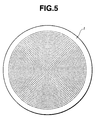
- a portion 1 of an electrode sample to be consumed by plasma shown in Figs. 5 and 6, was prepared by machining a single crystal silicon member doped with P-type boron (resistance: 15 ⁇ cm) into a size (thickness: 7 mm, diameter: 223.5 mm), forming holes (diameter: 0.84 mm) in the number of 3025 pieces in the surface of the member by drilling, and polishing the surface using a lapping machine. Also, a portion 1 to be consumed by plasma was prepared using a glassy carbon plate (concentration of impurities: 2 ppm, thickness: 5 mm) in the same manner as described above.
- a portion 2 of the electrode sample not to be consumed by plasma shown in Fig. 6, was prepared by machining an isotropic graphite member (density: 1.82 g/cm 3 ) into a ring shape (outside diameter: 241.5 mm, thickness: 19.05 mm), coating the entire surface of the ring-shaped graphite member with a polycarbodiimide resin by vacuum impregnation and spraying, putting the resultant in a baking furnace, and baking the polycarbodiimide resin in an inert atmosphere at a temperature of 2000°C.
- the thickness of the glassy carbon material film was 5 ⁇ m.
- Each of the portions 1 was joined to the portion 2 by brazing using an indium filler, to thus obtain the electrode sample.
- Electrode samples were prepared by repeating the procedures of Examples 1 and 2, except that an isotropic graphite member not covered with a glassy carbon material was used as the portion 2 not to be consumed by plasma. In addition, an electrode sample, which was entirely formed of silicon, was prepared.
- each of the above electrode samples was set into a plasma etching system, and an oxide film on a silicon wafer (diameter: 8 inch) was etched by plasma using a mixed gas of trifluoromethane as a reaction gas, argon and oxygen. After this etching, the number of particles (particle size: 0.3 ⁇ m or more) adhering on the surface of the wafer was counted. The results are shown in Table 1.
Landscapes
- Chemical & Material Sciences (AREA)
- Engineering & Computer Science (AREA)
- Physics & Mathematics (AREA)
- Plasma & Fusion (AREA)
- Analytical Chemistry (AREA)
- Materials Engineering (AREA)
- Mechanical Engineering (AREA)
- Metallurgy (AREA)
- Organic Chemistry (AREA)
- Drying Of Semiconductors (AREA)
- ing And Chemical Polishing (AREA)
Applications Claiming Priority (3)
| Application Number | Priority Date | Filing Date | Title |
|---|---|---|---|
| JP12407496 | 1996-04-22 | ||
| JP124074/96 | 1996-04-22 | ||
| JP12407496A JP3454333B2 (ja) | 1996-04-22 | 1996-04-22 | プラズマエッチング電極 |
Publications (3)
| Publication Number | Publication Date |
|---|---|
| EP0803897A2 true EP0803897A2 (de) | 1997-10-29 |
| EP0803897A3 EP0803897A3 (de) | 1998-04-01 |
| EP0803897B1 EP0803897B1 (de) | 2002-09-11 |
Family
ID=14876298
Family Applications (1)
| Application Number | Title | Priority Date | Filing Date |
|---|---|---|---|
| EP97302745A Expired - Lifetime EP0803897B1 (de) | 1996-04-22 | 1997-04-22 | Elektrode für Plasmaätzen; Vorrichtung und Verfahren mit dieser Elektrode |
Country Status (6)
| Country | Link |
|---|---|
| US (1) | US5951814A (de) |
| EP (1) | EP0803897B1 (de) |
| JP (1) | JP3454333B2 (de) |
| KR (1) | KR100417926B1 (de) |
| DE (1) | DE69715289T2 (de) |
| TW (1) | TW379257B (de) |
Cited By (2)
| Publication number | Priority date | Publication date | Assignee | Title |
|---|---|---|---|---|
| WO2001088966A3 (en) * | 2000-05-12 | 2002-03-28 | Tokyo Electron Ltd | Method of adjusting the thickness of an electrode in a plasma processing system |
| EP1357576A3 (de) * | 2002-04-22 | 2006-04-26 | Nisshinbo Industries, Inc. | Hitzebeständige Elektrode zum Plasmaätzen, und Plasmaätzvorrichtung mit dieser Elektrode |
Families Citing this family (16)
| Publication number | Priority date | Publication date | Assignee | Title |
|---|---|---|---|---|
| US6399499B1 (en) * | 1999-09-14 | 2002-06-04 | Jeong Gey Lee | Method for fabricating an electrode of a plasma chamber |
| JP2002093777A (ja) * | 2000-07-11 | 2002-03-29 | Nisshinbo Ind Inc | ドライエッチング装置 |
| JP3876167B2 (ja) * | 2002-02-13 | 2007-01-31 | 川崎マイクロエレクトロニクス株式会社 | 洗浄方法および半導体装置の製造方法 |
| US6846726B2 (en) * | 2002-04-17 | 2005-01-25 | Lam Research Corporation | Silicon parts having reduced metallic impurity concentration for plasma reaction chambers |
| US20040033361A1 (en) * | 2002-08-06 | 2004-02-19 | Kabushiki Kaisha Kobe Seiko Sho(Kobe Steel, Ltd.) | Component of glass-like carbon for CVD apparatus and process for production thereof |
| US7172531B2 (en) * | 2003-06-06 | 2007-02-06 | Rodgers Jr Robert E | Variable stride exercise apparatus |
| JP4403919B2 (ja) * | 2004-04-01 | 2010-01-27 | 株式会社Sumco | 耐久性に優れたプラズマエッチング用シリコン電極板 |
| US7247579B2 (en) | 2004-12-23 | 2007-07-24 | Lam Research Corporation | Cleaning methods for silicon electrode assembly surface contamination removal |
| JP4849236B2 (ja) * | 2006-09-27 | 2012-01-11 | 三菱マテリアル株式会社 | パーティクル発生の少ないプラズマエッチング装置用シリコン電極板 |
| KR101553422B1 (ko) * | 2007-12-19 | 2015-09-15 | 램 리써치 코포레이션 | 플라즈마 처리 장치를 위한 복합 샤워헤드 전극 어셈블리 |
| KR101553423B1 (ko) * | 2007-12-19 | 2015-09-15 | 램 리써치 코포레이션 | 반도체 진공 프로세싱 장치용 필름 점착제 |
| GB2465174A (en) * | 2008-11-06 | 2010-05-12 | Nviro Cleantech Ltd | Roughened electrode for decontamination processes |
| GB201102337D0 (en) * | 2011-02-09 | 2011-03-23 | Univ Ulster | A plasma based surface augmentation method |
| US9314854B2 (en) | 2013-01-30 | 2016-04-19 | Lam Research Corporation | Ductile mode drilling methods for brittle components of plasma processing apparatuses |
| US8893702B2 (en) | 2013-02-20 | 2014-11-25 | Lam Research Corporation | Ductile mode machining methods for hard and brittle components of plasma processing apparatuses |
| US20140356985A1 (en) | 2013-06-03 | 2014-12-04 | Lam Research Corporation | Temperature controlled substrate support assembly |
Family Cites Families (9)
| Publication number | Priority date | Publication date | Assignee | Title |
|---|---|---|---|---|
| JPS61224423A (ja) * | 1985-03-29 | 1986-10-06 | Toshiba Corp | 反応性イオンエツチング装置 |
| JP2553389B2 (ja) * | 1988-12-26 | 1996-11-13 | 東芝セラミックス株式会社 | Cvd装置用カーボン治具 |
| JPH07114198B2 (ja) * | 1989-10-02 | 1995-12-06 | 東海カーボン株式会社 | プラズマエッチング用電極板 |
| JPH0826464B2 (ja) * | 1989-10-20 | 1996-03-13 | イビデン株式会社 | プラズマエツチング用電極板 |
| JPH0463606A (ja) * | 1990-07-03 | 1992-02-28 | Nippon Steel Corp | 表面に非晶質炭素層を持つダイヤモンド工具 |
| JP3252330B2 (ja) * | 1991-09-20 | 2002-02-04 | 東芝セラミックス株式会社 | プラズマエッチング用電極板 |
| JP2527666B2 (ja) * | 1992-02-18 | 1996-08-28 | イビデン株式会社 | ガラス状炭素被覆物品 |
| US5472565A (en) * | 1993-11-17 | 1995-12-05 | Lam Research Corporation | Topology induced plasma enhancement for etched uniformity improvement |
| JP3372647B2 (ja) * | 1994-04-18 | 2003-02-04 | キヤノン株式会社 | プラズマ処理装置 |
-
1996
- 1996-04-22 JP JP12407496A patent/JP3454333B2/ja not_active Expired - Fee Related
-
1997
- 1997-04-17 TW TW086104970A patent/TW379257B/zh not_active IP Right Cessation
- 1997-04-18 US US08/837,468 patent/US5951814A/en not_active Expired - Lifetime
- 1997-04-21 KR KR1019970014667A patent/KR100417926B1/ko not_active Expired - Fee Related
- 1997-04-22 EP EP97302745A patent/EP0803897B1/de not_active Expired - Lifetime
- 1997-04-22 DE DE69715289T patent/DE69715289T2/de not_active Expired - Fee Related
Cited By (3)
| Publication number | Priority date | Publication date | Assignee | Title |
|---|---|---|---|---|
| WO2001088966A3 (en) * | 2000-05-12 | 2002-03-28 | Tokyo Electron Ltd | Method of adjusting the thickness of an electrode in a plasma processing system |
| US6913703B2 (en) | 2000-05-12 | 2005-07-05 | Tokyo Electron Limited | Method of adjusting the thickness of an electrode in a plasma processing system |
| EP1357576A3 (de) * | 2002-04-22 | 2006-04-26 | Nisshinbo Industries, Inc. | Hitzebeständige Elektrode zum Plasmaätzen, und Plasmaätzvorrichtung mit dieser Elektrode |
Also Published As
| Publication number | Publication date |
|---|---|
| US5951814A (en) | 1999-09-14 |
| EP0803897A3 (de) | 1998-04-01 |
| DE69715289T2 (de) | 2003-05-08 |
| KR970070241A (ko) | 1997-11-07 |
| EP0803897B1 (de) | 2002-09-11 |
| JP3454333B2 (ja) | 2003-10-06 |
| JPH09289197A (ja) | 1997-11-04 |
| KR100417926B1 (ko) | 2004-06-11 |
| DE69715289D1 (de) | 2002-10-17 |
| TW379257B (en) | 2000-01-11 |
Similar Documents
| Publication | Publication Date | Title |
|---|---|---|
| EP0803897B1 (de) | Elektrode für Plasmaätzen; Vorrichtung und Verfahren mit dieser Elektrode | |
| KR100596085B1 (ko) | 챔버 내벽 보호 부재 및 플라즈마 처리 장치 | |
| US7517803B2 (en) | Silicon parts having reduced metallic impurity concentration for plasma reaction chambers | |
| CN1809513A (zh) | 精加工石英玻璃表面的方法和所述方法生产的部件 | |
| US20070217114A1 (en) | Electrostatic chuck | |
| JP4837894B2 (ja) | シリコン部品の形成方法 | |
| EP0803895A2 (de) | Elektrode für Plasmaätzen | |
| EP0803896B1 (de) | Plasmabehandlungsvorrichtung und Schutzteil dafür | |
| JP2000049144A (ja) | プラズマ処理装置用電極板 | |
| JP3444089B2 (ja) | プラズマエッチング電極 | |
| JPH06128762A (ja) | プラズマエッチング用電極板 | |
| JPH08134667A (ja) | プラズマエッチング用陽極電極板 | |
| JPH09245994A (ja) | プラズマ利用の加工装置用電極およびその電極の製造方法 | |
| EP0663687B1 (de) | Vorrichtung und Verfahren zur Herstellung von Halbleitern | |
| JP3317148B2 (ja) | プラズマエッチング電極の製造方法 | |
| JPH09289195A (ja) | プラズマエッチング電極 | |
| JP2002353425A (ja) | サファイア基板およびその製造方法 | |
| JPH07273094A (ja) | プラズマエッチング用電極板 | |
| JP2000040689A (ja) | プラズマエッチング用電極板 | |
| JP3631368B2 (ja) | プラズマエッチング電極及びそれを用いたプラズマエッチング装置 | |
| JPS63169243A (ja) | 真空吸着装置 | |
| JP2000021852A (ja) | プラズマエッチング電極及びプラズマエッチング装置 | |
| JPH09289199A (ja) | プラズマエッチング電極 | |
| JP2002075962A (ja) | シリコンウェハー搭載用ガラス状カーボン−グラファイト複合リング及びそれを装着したドライエッチング装置 | |
| JPH10199862A (ja) | プラズマ処理装置用保護部材及び該保護部材を使用したプラズマ処理装置 |
Legal Events
| Date | Code | Title | Description |
|---|---|---|---|
| PUAI | Public reference made under article 153(3) epc to a published international application that has entered the european phase |
Free format text: ORIGINAL CODE: 0009012 |
|
| AK | Designated contracting states |
Kind code of ref document: A2 Designated state(s): DE FR GB |
|
| PUAL | Search report despatched |
Free format text: ORIGINAL CODE: 0009013 |
|
| AK | Designated contracting states |
Kind code of ref document: A3 Designated state(s): DE FR GB |
|
| 17P | Request for examination filed |
Effective date: 19980429 |
|
| 17Q | First examination report despatched |
Effective date: 19991214 |
|
| GRAG | Despatch of communication of intention to grant |
Free format text: ORIGINAL CODE: EPIDOS AGRA |
|
| RTI1 | Title (correction) |
Free format text: ELECTRODE FOR PLASMA ETCHING; APPARATUS AND PROCESS USING SUCH ELECTRODE |
|
| GRAG | Despatch of communication of intention to grant |
Free format text: ORIGINAL CODE: EPIDOS AGRA |
|
| GRAH | Despatch of communication of intention to grant a patent |
Free format text: ORIGINAL CODE: EPIDOS IGRA |
|
| GRAH | Despatch of communication of intention to grant a patent |
Free format text: ORIGINAL CODE: EPIDOS IGRA |
|
| GRAA | (expected) grant |
Free format text: ORIGINAL CODE: 0009210 |
|
| AK | Designated contracting states |
Kind code of ref document: B1 Designated state(s): DE FR GB |
|
| REG | Reference to a national code |
Ref country code: GB Ref legal event code: FG4D |
|
| REF | Corresponds to: |
Ref document number: 69715289 Country of ref document: DE Date of ref document: 20021017 |
|
| ET | Fr: translation filed | ||
| PLBE | No opposition filed within time limit |
Free format text: ORIGINAL CODE: 0009261 |
|
| STAA | Information on the status of an ep patent application or granted ep patent |
Free format text: STATUS: NO OPPOSITION FILED WITHIN TIME LIMIT |
|
| 26N | No opposition filed |
Effective date: 20030612 |
|
| PG25 | Lapsed in a contracting state [announced via postgrant information from national office to epo] |
Ref country code: FR Free format text: LAPSE BECAUSE OF NON-PAYMENT OF DUE FEES Effective date: 20031231 |
|
| REG | Reference to a national code |
Ref country code: FR Ref legal event code: ST |
|
| PGFP | Annual fee paid to national office [announced via postgrant information from national office to epo] |
Ref country code: GB Payment date: 20070418 Year of fee payment: 11 |
|
| PGFP | Annual fee paid to national office [announced via postgrant information from national office to epo] |
Ref country code: DE Payment date: 20080502 Year of fee payment: 12 |
|
| GBPC | Gb: european patent ceased through non-payment of renewal fee |
Effective date: 20080422 |
|
| PG25 | Lapsed in a contracting state [announced via postgrant information from national office to epo] |
Ref country code: GB Free format text: LAPSE BECAUSE OF NON-PAYMENT OF DUE FEES Effective date: 20080422 |
|
| PG25 | Lapsed in a contracting state [announced via postgrant information from national office to epo] |
Ref country code: DE Free format text: LAPSE BECAUSE OF NON-PAYMENT OF DUE FEES Effective date: 20091103 |