EP0802571A2 - Dispositif semi-conducteur comprenant un transistor à effet de champ et procédé de fabrication - Google Patents
Dispositif semi-conducteur comprenant un transistor à effet de champ et procédé de fabrication Download PDFInfo
- Publication number
- EP0802571A2 EP0802571A2 EP97106579A EP97106579A EP0802571A2 EP 0802571 A2 EP0802571 A2 EP 0802571A2 EP 97106579 A EP97106579 A EP 97106579A EP 97106579 A EP97106579 A EP 97106579A EP 0802571 A2 EP0802571 A2 EP 0802571A2
- Authority
- EP
- European Patent Office
- Prior art keywords
- field effect
- effect transistor
- source
- drain
- electrode
- Prior art date
- Legal status (The legal status is an assumption and is not a legal conclusion. Google has not performed a legal analysis and makes no representation as to the accuracy of the status listed.)
- Withdrawn
Links
Images

Classifications
-
- H—ELECTRICITY
- H10—SEMICONDUCTOR DEVICES; ELECTRIC SOLID-STATE DEVICES NOT OTHERWISE PROVIDED FOR
- H10F—INORGANIC SEMICONDUCTOR DEVICES SENSITIVE TO INFRARED RADIATION, LIGHT, ELECTROMAGNETIC RADIATION OF SHORTER WAVELENGTH OR CORPUSCULAR RADIATION
- H10F30/00—Individual radiation-sensitive semiconductor devices in which radiation controls the flow of current through the devices, e.g. photodetectors
- H10F30/20—Individual radiation-sensitive semiconductor devices in which radiation controls the flow of current through the devices, e.g. photodetectors the devices having potential barriers, e.g. phototransistors
- H10F30/21—Individual radiation-sensitive semiconductor devices in which radiation controls the flow of current through the devices, e.g. photodetectors the devices having potential barriers, e.g. phototransistors the devices being sensitive to infrared, visible or ultraviolet radiation
- H10F30/28—Individual radiation-sensitive semiconductor devices in which radiation controls the flow of current through the devices, e.g. photodetectors the devices having potential barriers, e.g. phototransistors the devices being sensitive to infrared, visible or ultraviolet radiation the devices being characterised by field-effect operation, e.g. junction field-effect phototransistors
-
- H—ELECTRICITY
- H10—SEMICONDUCTOR DEVICES; ELECTRIC SOLID-STATE DEVICES NOT OTHERWISE PROVIDED FOR
- H10F—INORGANIC SEMICONDUCTOR DEVICES SENSITIVE TO INFRARED RADIATION, LIGHT, ELECTROMAGNETIC RADIATION OF SHORTER WAVELENGTH OR CORPUSCULAR RADIATION
- H10F71/00—Manufacture or treatment of devices covered by this subclass
Definitions
- the present invention relates to a semiconductor component with a substrate and with a field effect transistor or a field effect transistor formed on the substrate, in which a current flowing through a conductive semiconductor channel between a source electrode and a drain electrode via a field acting perpendicularly on the channel between at least one Gate electrode and the channel is controllable and has a relatively large active transistor area.
- Such semiconductor devices include, for. B. simple field-effect transistors (FETs), metal-semiconductor field-effect transistors (MESFETs), which work on the principle of the junction field-effect transistor, in which a Schottky junction is used instead of the controlling pn junction, field-effect transistors with a metal-insulator-semiconductor junction (MISFETs) .
- FETs simple field-effect transistors
- MOSFETs metal-semiconductor field-effect transistors
- MISFETs metal-insulator-semiconductor junction
- the gate length of an electrically controlled high frequency transistor is of the order of 1 ⁇ m. Therefore, several gates have to be arranged in parallel in order to obtain a useful active transistor area. In order to contact source, gate and drain strips of such an arrangement, isolation layers or air bridges are required in the conventional technology designed for minimal gate metallization resistance.
- Optoelectronically controlled components such as. B.
- optoelectronic receivers usually consist of an optoelectronic detector (eg MSM or PIN diode) and a subsequent electrical amplifier circuit.
- the electrical connection between the receiver and the amplifier deteriorates the properties of the receiver due to parasitic resistances, inductances and capacitances and through noise contributions.
- By integrating the optoelectronic detector and the first amplifier stage This reduction in quality can be prevented in a component.
- the manufacturing effort is reduced.
- One such component is the OPFET.
- the light reaches the control zone of a field effect transistor through a transparent or semi-transparent gate or through the back of the wafer, where it generates electron-hole pairs.
- the drain current of the transistor is influenced by this electrical change in the gate control path.
- the resistance of the gate metallization in the OPFET plays no role for the speed because the electrical excitation takes place inside the transistor. Therefore, in contrast to the classic transistor, the transistor design does not need to be optimized for a minimal gate resistance.
- the conventional design is disadvantageous at least for this type of use of the field effect transistors.
- the object of the present invention is therefore to provide a semiconductor component or a field effect transistor which has a relatively large active transistor area with a structurally simple construction.
- the object is achieved according to claim 1 in that the source electrode, the drain electrode and the gate electrode are designed without crossover and according to claim 7 by a field effect transistor with crossover-free source, drain and gate electrodes.
- Another object of the present invention is to provide a method for easier manufacture of a semiconductor component with a field effect transistor.
- This object is achieved by etching the transistor to define a transistor area: applying an ohmic source and drain metallization to a surface layer; at least partially etching away the surface layer and underetching the metallizations of source and drain; self-aligned application of a gate electrode; Application of contact connections.
- the light to be detected e.g. A glass fiber usually has a spot diameter of a few 10 ⁇ m.
- Conventional MSM detectors have an area of typically 50 ⁇ m x 50 ⁇ m to collect a large part of the light from the glass fiber and to facilitate the adjustment of the glass fiber.
- the active transistor area of an OPFET should therefore also have approximately these dimensions.
- a particularly favorable mode of operation of the semiconductor component is achieved if, according to claims 2 and 8, the gate electrode is meandering and the source and drain electrodes are each interdigitated.
- the method according to the invention has the advantage that the use of a self-adjusting process and the mode of operation of the source and drain electrodes as a mask for the application of the gate electrode make production much easier.
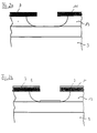
- a conductive semiconductor channel 5 is formed on a substrate 3 in accordance with the field effect transistor used (FET, MESFET, MISFET, MOSFET, HEMT).
- FET field effect transistor used
- MESFET MESFET
- MISFET MISFET
- MOSFET MOSFET
- HEMT HEMT
- a gate electrode 7 with a gate terminal 7.1 is arranged in a meandering form.
- a source electrode 9 with a source terminal 9.1 extends finger-shaped on the left side in FIG. 1, and a corresponding finger-shaped drain electrode 11 with a drain terminal 11.1 extends on the right side in FIG. 1.
- the source electrode 9 and drain electrode 11 are aligned in this way that the trained fingers interlock.
- the gate electrode 7 is made of a transparent or semi-transparent material.
- the component 1 should have an approximately square active transistor area, preferably in a size of 50 ⁇ m ⁇ 50 ⁇ m. In other embodiments, however, the active transistor area can also have other dimensions which are adapted to the respective requirements.
- the gate 7 of a field effect transistor is designed as a meander, with finger-shaped source and drain electrodes 9, 11 of a component 1.
- the aim of this layout is a more or less square active area of the component 1 to receive the light from a light spot, e.g. from a fiber optic cable, to be used as effectively as possible.
- the gate 7 of the component 1 should be made of transparent or semitransparent material in order to guide the light to be detected through the gate metallization into the transistor zone with a control effect.
- the component 1 is to be produced using a self-adjusting process, the finger-shaped source and drain electrodes 9, 11 serving as a mask for the application of the gate electrode 7.
Landscapes
- Junction Field-Effect Transistors (AREA)
Applications Claiming Priority (2)
| Application Number | Priority Date | Filing Date | Title |
|---|---|---|---|
| DE19615495A DE19615495C2 (de) | 1996-04-19 | 1996-04-19 | Halbleiter-Bauelement und Verfahren zu dessen Herstellung |
| DE19615495 | 1996-04-19 |
Publications (2)
| Publication Number | Publication Date |
|---|---|
| EP0802571A2 true EP0802571A2 (fr) | 1997-10-22 |
| EP0802571A3 EP0802571A3 (fr) | 1998-10-21 |
Family
ID=7791748
Family Applications (1)
| Application Number | Title | Priority Date | Filing Date |
|---|---|---|---|
| EP97106579A Withdrawn EP0802571A3 (fr) | 1996-04-19 | 1997-04-21 | Dispositif semi-conducteur comprenant un transistor à effet de champ et procédé de fabrication |
Country Status (2)
| Country | Link |
|---|---|
| EP (1) | EP0802571A3 (fr) |
| DE (1) | DE19615495C2 (fr) |
Cited By (2)
| Publication number | Priority date | Publication date | Assignee | Title |
|---|---|---|---|---|
| CN100336096C (zh) * | 2001-12-26 | 2007-09-05 | Lg.飞利浦Lcd有限公司 | 液晶显示器的数据驱动装置及方法 |
| US7939866B2 (en) | 2007-05-21 | 2011-05-10 | Rfmd (Uk) Limited | Field effect transistor |
Families Citing this family (1)
| Publication number | Priority date | Publication date | Assignee | Title |
|---|---|---|---|---|
| DE102011075103B4 (de) | 2011-05-02 | 2014-04-10 | Forschungsverbund Berlin E.V. | Photodetektor |
Family Cites Families (3)
| Publication number | Priority date | Publication date | Assignee | Title |
|---|---|---|---|---|
| US4351706A (en) * | 1980-03-27 | 1982-09-28 | International Business Machines Corporation | Electrochemically eroding semiconductor device |
| EP0373803A3 (fr) * | 1988-12-16 | 1991-07-10 | Raytheon Company | Circuits commutateurs en R.F. |
| US5453630A (en) * | 1992-11-12 | 1995-09-26 | The United States Of America As Represented By The Secretary Of The Army | Variable gain optical detector |
-
1996
- 1996-04-19 DE DE19615495A patent/DE19615495C2/de not_active Expired - Fee Related
-
1997
- 1997-04-21 EP EP97106579A patent/EP0802571A3/fr not_active Withdrawn
Cited By (3)
| Publication number | Priority date | Publication date | Assignee | Title |
|---|---|---|---|---|
| CN100336096C (zh) * | 2001-12-26 | 2007-09-05 | Lg.飞利浦Lcd有限公司 | 液晶显示器的数据驱动装置及方法 |
| US7436384B2 (en) | 2001-12-26 | 2008-10-14 | Lg Display Co., Ltd. | Data driving apparatus and method for liquid crystal display |
| US7939866B2 (en) | 2007-05-21 | 2011-05-10 | Rfmd (Uk) Limited | Field effect transistor |
Also Published As
| Publication number | Publication date |
|---|---|
| DE19615495A1 (de) | 1997-10-23 |
| DE19615495C2 (de) | 1999-07-22 |
| EP0802571A3 (fr) | 1998-10-21 |
Similar Documents
| Publication | Publication Date | Title |
|---|---|---|
| DE69224709T2 (de) | Halbleiteranordnung mit verbesserter Durchbruchspannungs-Charakteristik | |
| DE3121224C2 (de) | MOS-Transistor für hohe Betriebsspannungen | |
| DE69935182T2 (de) | Halbleiteranordnung | |
| DE69108631T2 (de) | Tunnelinjektions-Halbleiterbauelement und dessen Herstellungsverfahren. | |
| DE19823069B4 (de) | Halbleiterbauelement | |
| DE69602632T2 (de) | Feldeffekttransistor mit Kammstruktur | |
| DE69534581T2 (de) | Feld-Effekt-Halbleiterbauelement und sein Herstellungsverfahren | |
| DE10250832B4 (de) | MOS-Transistor auf SOI-Substrat mit Source-Durchkontaktierung und Verfahren zur Herstellung eines solchen Transistors | |
| DE69629017T2 (de) | Laterale dünnfilm-soi-anordnungen mit einem gradierten feldoxid und linearem dopierungsprofil | |
| DE69530716T2 (de) | Beschleunigungssensor und Verfahren zu seiner Herstellung | |
| DE3145230A1 (de) | "halbleiteranordnung" | |
| DE10343509A1 (de) | Halbleiteranordnung | |
| EP0750352A2 (fr) | Configuration d'un dispositif semi-conducteur | |
| DE69329097T2 (de) | Neue Anordnung für eine Vorrichtung mit vielen HV-LDMOS Transistoren und einer Schaltung innerhalb einer schwebenden Wanne | |
| DE4118188A1 (de) | Laterale dmosfet-halbleitereinrichtung mit reduziertem durchlasswiderstand und geringen abmessungen | |
| DE2300116B2 (de) | Hochfrequenz-Feldeffekttransistor mit isolierter Gate-Elektrode für Breitbandbetrieb | |
| EP1336989B1 (fr) | Dispositif transistor | |
| DE10137343C1 (de) | Halbleiterstruktur mit Feldplatte | |
| DE69026675T2 (de) | MIS-Kapazitätselement | |
| EP0716453B1 (fr) | MOSFET sur substrat du type SOI | |
| DE3142644C2 (de) | Halbleiteranordnung mit in einem Halbleiterkörper angeordneten Bipolartransistor und Diode | |
| DE1639349C3 (de) | Feldeffekt-Transistor mit isolierter Gate-Elektrode, Verfahren zu seiner Herstellung und Verwendung eines solchen Feldeffekt-Transistors in einer integrierten Schaltung | |
| DE112007000161B4 (de) | Multifinger-FET für Hochfrequenz | |
| DE19615495C2 (de) | Halbleiter-Bauelement und Verfahren zu dessen Herstellung | |
| DE19710731B4 (de) | Leistungshalbleiterbauteil und Verfahren zu dessen Herstellung |
Legal Events
| Date | Code | Title | Description |
|---|---|---|---|
| PUAI | Public reference made under article 153(3) epc to a published international application that has entered the european phase |
Free format text: ORIGINAL CODE: 0009012 |
|
| AK | Designated contracting states |
Kind code of ref document: A2 Designated state(s): AT BE CH DE FR GB IT LI LU NL SE |
|
| PUAL | Search report despatched |
Free format text: ORIGINAL CODE: 0009013 |
|
| AK | Designated contracting states |
Kind code of ref document: A3 Designated state(s): AT BE CH DE FR GB IT LI LU NL SE |
|
| 17P | Request for examination filed |
Effective date: 19990115 |
|
| RAP1 | Party data changed (applicant data changed or rights of an application transferred) |
Owner name: FORSCHUNGSZENTRUM JUELICH GMBH |
|
| STAA | Information on the status of an ep patent application or granted ep patent |
Free format text: STATUS: THE APPLICATION IS DEEMED TO BE WITHDRAWN |
|
| 18D | Application deemed to be withdrawn |
Effective date: 20031101 |