EP0794477A1 - Schaltung zur Spannungserzeugung - Google Patents
Schaltung zur Spannungserzeugung Download PDFInfo
- Publication number
- EP0794477A1 EP0794477A1 EP97106656A EP97106656A EP0794477A1 EP 0794477 A1 EP0794477 A1 EP 0794477A1 EP 97106656 A EP97106656 A EP 97106656A EP 97106656 A EP97106656 A EP 97106656A EP 0794477 A1 EP0794477 A1 EP 0794477A1
- Authority
- EP
- European Patent Office
- Prior art keywords
- voltage
- input
- reference voltage
- circuit
- voltages
- Prior art date
- Legal status (The legal status is an assumption and is not a legal conclusion. Google has not performed a legal analysis and makes no representation as to the accuracy of the status listed.)
- Withdrawn
Links
- 238000001514 detection method Methods 0.000 description 50
- 239000002131 composite material Substances 0.000 description 37
- 239000003990 capacitor Substances 0.000 description 19
- 230000007935 neutral effect Effects 0.000 description 11
- 238000010586 diagram Methods 0.000 description 9
- 238000001914 filtration Methods 0.000 description 7
- 230000000694 effects Effects 0.000 description 5
- 238000009499 grossing Methods 0.000 description 4
- 238000010304 firing Methods 0.000 description 3
- 238000000034 method Methods 0.000 description 3
- 230000000630 rising effect Effects 0.000 description 3
- 238000004364 calculation method Methods 0.000 description 2
- 230000015556 catabolic process Effects 0.000 description 2
- 230000001276 controlling effect Effects 0.000 description 2
- 238000004519 manufacturing process Methods 0.000 description 2
- 238000005259 measurement Methods 0.000 description 2
- 230000008859 change Effects 0.000 description 1
- 230000007812 deficiency Effects 0.000 description 1
- 230000009977 dual effect Effects 0.000 description 1
- 238000013213 extrapolation Methods 0.000 description 1
- 230000007246 mechanism Effects 0.000 description 1
- 238000004377 microelectronic Methods 0.000 description 1
- 230000009467 reduction Effects 0.000 description 1
- 230000001105 regulatory effect Effects 0.000 description 1
- 238000000926 separation method Methods 0.000 description 1
- 230000002123 temporal effect Effects 0.000 description 1
Images


Classifications
-
- G—PHYSICS
- G05—CONTROLLING; REGULATING
- G05F—SYSTEMS FOR REGULATING ELECTRIC OR MAGNETIC VARIABLES
- G05F3/00—Non-retroactive systems for regulating electric variables by using an uncontrolled element, or an uncontrolled combination of elements, such element or such combination having self-regulating properties
- G05F3/02—Regulating voltage or current
- G05F3/08—Regulating voltage or current wherein the variable is DC
- G05F3/10—Regulating voltage or current wherein the variable is DC using uncontrolled devices with non-linear characteristics
- G05F3/16—Regulating voltage or current wherein the variable is DC using uncontrolled devices with non-linear characteristics being semiconductor devices
- G05F3/20—Regulating voltage or current wherein the variable is DC using uncontrolled devices with non-linear characteristics being semiconductor devices using diode- transistor combinations
- G05F3/24—Regulating voltage or current wherein the variable is DC using uncontrolled devices with non-linear characteristics being semiconductor devices using diode- transistor combinations wherein the transistors are of the field-effect type only
- G05F3/242—Regulating voltage or current wherein the variable is DC using uncontrolled devices with non-linear characteristics being semiconductor devices using diode- transistor combinations wherein the transistors are of the field-effect type only with compensation for device parameters, e.g. channel width modulation, threshold voltage, processing, or external variations, e.g. temperature, loading, supply voltage
- G05F3/247—Regulating voltage or current wherein the variable is DC using uncontrolled devices with non-linear characteristics being semiconductor devices using diode- transistor combinations wherein the transistors are of the field-effect type only with compensation for device parameters, e.g. channel width modulation, threshold voltage, processing, or external variations, e.g. temperature, loading, supply voltage producing a voltage or current as a predetermined function of the supply voltage
-
- G—PHYSICS
- G05—CONTROLLING; REGULATING
- G05F—SYSTEMS FOR REGULATING ELECTRIC OR MAGNETIC VARIABLES
- G05F3/00—Non-retroactive systems for regulating electric variables by using an uncontrolled element, or an uncontrolled combination of elements, such element or such combination having self-regulating properties
- G05F3/02—Regulating voltage or current
- G05F3/08—Regulating voltage or current wherein the variable is DC
- G05F3/10—Regulating voltage or current wherein the variable is DC using uncontrolled devices with non-linear characteristics
- G05F3/16—Regulating voltage or current wherein the variable is DC using uncontrolled devices with non-linear characteristics being semiconductor devices
- G05F3/20—Regulating voltage or current wherein the variable is DC using uncontrolled devices with non-linear characteristics being semiconductor devices using diode- transistor combinations
- G05F3/24—Regulating voltage or current wherein the variable is DC using uncontrolled devices with non-linear characteristics being semiconductor devices using diode- transistor combinations wherein the transistors are of the field-effect type only
-
- H—ELECTRICITY
- H02—GENERATION; CONVERSION OR DISTRIBUTION OF ELECTRIC POWER
- H02M—APPARATUS FOR CONVERSION BETWEEN AC AND AC, BETWEEN AC AND DC, OR BETWEEN DC AND DC, AND FOR USE WITH MAINS OR SIMILAR POWER SUPPLY SYSTEMS; CONVERSION OF DC OR AC INPUT POWER INTO SURGE OUTPUT POWER; CONTROL OR REGULATION THEREOF
- H02M1/00—Details of apparatus for conversion
- H02M1/10—Arrangements incorporating converting means for enabling loads to be operated at will from different kinds of power supplies, e.g. from AC or DC
Definitions
- the present invention relates to a DC supply circuit, particularly but not exclusively for use in mains powered equipment which detects the magnitude of the mains voltage applied and accordingly adjusts the operation of associated rectifier circuitry.
- FIGS 1A and 1B illustrate a manually operated doubler/bridge switch.
- Four diodes D 1 -D 4 are connected together as bridge rectifier.
- An AC input voltage V LN is applied between nodes 2, 4, where node 2 is connected to the anode of D 1 and the cathode of D 2 , and node 4 is connected to the anode of D 3 and the cathode of D 4 .
- Two capacitors C 1 , C 2 are connected in series between nodes 6, 8, being the DC output nodes of the bridge rectifier.
- a load L is connected between nodes 6, 8 and is supplied with the DC output.
- a switch T is connected between node 4 and node 10, being the node between the two capacitors.
- diodes D 1 -D 4 form a conventional bridge rectifier with capacitors C 1 , C 2 to smooth the DC output generated. This is the bridge rectification mode.
- diodes D 1 , D 2 and capacitors C 1 , C 2 operate as a combined voltage doubler and rectifier circuit of the known type. Diodes D 3 , D 4 are superfluous in this mode. This is the voltage doubling rectification mode.
- An automatic doubler/bridge switch circuit which automatically doubles and rectifies a low range AC input voltage and which merely rectifies a high range AC input voltage. Sensing of the voltage level of the mains may be done by detecting peak voltage values of the AC waveform and using voltage comparators, or by sensing the magnitude of a DC rectified input voltage. Such circuits are available in either integrated circuit or discrete component form.
- a triac acts to conduct in either direction after the application of a negative (active low) pulse to its gate terminal, until the voltage across its two main terminals falls below a minimum value.
- a gate pulse soon after every mains zero crossing point, the triac approximates to a short circuit.
- the introduction of such a short circuit provides the changeover from the bridge rectification mode shown in figure 1A to the voltage doubling rectification mode shown in figure 1B.
- An alternating voltage is a voltage which undergoes successive upper and lower excursions, respectively more and less positive than a baseline voltage, such baseline voltage being the time average of the alternating voltage.
- the baseline voltage is at the ground (zero volts) level.
- the automatic voltage sensitive switch circuit described in the patent is a circuit containing several voltage comparators: these are used to detect peak voltage values to indicate a mains input AC voltage of the higher range, and to detect baseline crossing points to give timing information for triac gate pulses. Voltage reference sources are also built into the circuit to set the voltage reference points of the comparators. Means may be provided for generating many triac gate pulses per half-cycle of AC mains, to ensure efficient triggering in the presence of noise or disturbance on the AC lines. Filtering circuits may be included to remove such noise or disturbance from the voltage used for peak voltage detection.
- Such integrated circuits are small and reliable.
- the cost of an automatic voltage sensitive switch circuit is reduced by reducing the number of components required, external to the integrated circuit.
- Known automatic voltage sensitive switches employ a "single cycle" sensing mechanism, i.e. peak voltage level sensing is carried out on either only the upper or only the lower excursion of the mains voltage, linear extrapolation techniques being used to derive data for the other excursion.
- filtering, baseline crossing detection and peak voltage level sensing may only be carried out on a scaled representation of AC input voltages falling within a range limited by the two DC supply voltage levels of the control circuit of the automatic voltage sensitive switch. These are typically 0V and 9V.
- the AC input voltage is scaled down for input to the control circuit, but as it is centred on 0V, the mains baseline, only one of the upper and lower excursions of the scaled AC voltage will fall within the allowed range for peak voltage level sensing.
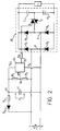
- a doubler/bridge circuit 20 includes a triac T switching element; nodes 2, 4 are connected to the live L and neutral N lines of the AC mains, and receive the AC input voltage V LN .
- a diode D 5 , a resistor R 4 and a capacitor C are respectively connected in series between the live line L and the neutral line N.
- Two resistors R 1 , R 2 are connected in series between the live line L and the node 22 between the capacitor C and the resistor R 4 .
- the voltage between the neutral line N and node 22 is the voltage V C across the capacitor C.
- the automatic voltage sensitive switch control circuit 24 receives a first input voltage V ss from the node 22 and a second input voltage V 4 from the neutral line N and a third, 'composite', input voltage, V M from the node 26 between resistors R 1 , R 2 , and supplies an output voltage V G T through a resistor R g to the gate G of the triac T.
- Diode D 5 , resistor R 4 and capacitor C form a half-wave rectifier and smoothing circuit and provide a DC supply voltage V C to the automatic voltage sensitive switch control circuit 24.
- V ss is taken as a ground voltage for the circuit. It is at a voltage V C less than the voltage of the neutral line N. (For example, 9V less as fixed by a regulator within the control circuit).
- the AC input voltage V LN is applied to the potential divider comprising resistors R 1 , R 2 .
- V LN + V C V 2 - V ss .
- V M (V 2 - V ss ) ⁇ R 2 R 1 +R 2 .
- V M R 2 (V LN +V C ) R 1 +R 2
- the DC offset of 0 ⁇ 16V means that the baseline of the composite voltage V M is at 0 ⁇ 16V, and baseline crossing points may be detected, including hysteresis, by detecting when V M crosses 0 ⁇ 05V and 0 ⁇ 25V, for example.
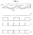
- FIGS 3 and 4 show example input and output signals for the known automatic voltage switches carrying out comparison operations on the input voltage described.
- a scaled AC input voltage V IN is clipped by the input protection devices to remain within the range R, to obtain a measurable composite voltage V M .
- a pulse PD is produced when V M exceeds a certain threshold voltage V TP .
- Pulses CS represent the times during which V M > 0V. The inverse of this signal is produced within the control circuit 24.
- a short pulse is produced at each rising edge of CS and its inverse, which are added to form the signal ZC, which indicates the baseline crossing points of V M , and hence the mains zero crossing points.
- Peak detection pulses PD are produced at the peak of every upper excursion for a high range AC input voltage, using a comparator whose switching threshold is set to detect a voltage V TP in excess of the peak voltage of the highest scaled AC voltage of the lower range.
- V TP may correspond to an instantaneous AC input voltage of 220V, the peak value of a 156Vrms AC input voltage.
- the threshold voltage must be carefully chosen, as AC mains voltages are subject to variation from time to time, resulting in the fact that the separation between a low range AC input voltage and a high range input voltage may be as small as 30Vrms (140Vrms to 170Vrms).
- Such peak detection pulses PD disable the generation of triac pulses V G T.
- no peak detection pulses PD are produced for low voltage AC input as the composite voltage V M never passes the V TP threshold.
- a comparator whose switching threshold is the baseline voltage level produces the comparison signal CS. Its inverse is also produced, and short pulses are generated at each rising edge of both CS and its inverse. The sum of these short pulses is the mains zero crossing indication signal ZC.
- Voltage level detection is limited to one excursion only per cycle due to input protection devices, which limit the composite voltage V M to the allowed range R in figures 3 and 4, being 0 ⁇ 6V either side of the supply voltages. This eliminates any possibility of performing measurements on the other excursion per cycle of the waveform, in this example, the negative excursion.
- Circuitry built into the control circuit 24 verifies a change in the apparent voltage range for at least two mains cycles before changing from bridge rectifier mode to voltage doubling rectification mode, so as to avoid the possibility of doubling a high range AC input voltage after a brief drop in AC input voltage.
- a temporal filter is included within the control circuit to reduce the effects of glitches, sags, spikes and voltage surges. This is only active on input voltages which lie within the range R.
- the filtering described is not effective on half the wave, leaving the control circuit vulnerable to damage caused by such transients on the unsensed portion of the AC input wave. To date, these deficiencies have been tolerated.
- Automatic voltage switching circuits also exist in discrete form, whereby the circuit contains a voltage comparator, with one input referenced to a zener diode, to detect rectified or scaled AC voltages above a certain upper or lower threshold, as defined by the zener diode, and circuitry to provide triac gate firing pulses when required.
- the object of the current invention is to provide a DC voltage supply circuit for rectifying an alternating voltage, using a minimum of discrete components, whilst improving sensing accuracy and reducing the circuit cost and complexity.
- the invention provides voltage level sensing during both positive and negative half cycles of the AC mains. This is achieved by adjusting the DC offset of the composite voltage, in order to bring the total composite voltage within the limits defined by the DC supply voltages, for the whole cycle of mains AC, and allow voltage level detection and filtering of the waveform over its whole cycle.
- a DC voltage supply circuit for rectifying an alternating voltage and supplying a DC output voltage at a substantially constant value.
- a voltage supply circuit includes: rectification circuitry for rectifying the alternating voltage; a voltage detection circuit for detecting, within upper and lower limits, peak values of said excursions for controlling said rectification circuitry; and a voltage shift circuit.
- the voltage shift circuit is arranged to receive the alternating voltage as an input, and connected to supply a composite voltage to the voltage detection circuit. It scales the input alternating voltage and shifts its baseline by a preselected DC bias, in order that the excursions fall within the upper and lower limits so that the voltage detection circuit is operable to detect peak values of both upper and lower excursions. If the input alternating voltage has a baseline other than at 0V, the baseline voltage will also be scaled and included in the scaled alternating input voltage.
- the composite voltage is the sum of the DC bias voltage and the scaled alternating input voltage.
- Such a DC voltage supply circuit may be operable within at least two distinct ranges of values of the alternating voltage.
- the output of the voltage detection circuit indicates the range containing the applied alternating voltage.
- the rectification circuitry has a number of modes equal to the number of distinct ranges of values of the alternating voltage, and the mode of operation of the rectification circuitry is selected according to the range indicated.
- Baseline crossing detection circuitry may be included to detect the times at which the input alternating voltage crosses its baseline; and the rectification circuit includes a switch, e.g. a triac, for selecting the mode of operation.
- the baseline detection circuitry is then used to generate control signals to the switch. These control signals are pulses when the switch is a triac.
- the rectification circuitry may be a doubler/bridge rectifier, with two modes of operation.
- the required preselected DC bias may be derived from DC supply voltages to the voltage detection circuit, while the scaled alternating input voltage may be provided by a resistive or capacitive divider network placed between the alternating input voltage and one of the voltage detection circuit supply voltages.
- the DC bias is then selected by controlling the DC current through one of the elements of the resistive divider.
- the voltage detection circuit preferably contains a plurality of voltage comparators, receiving a plurality of voltage references each corresponding to a threshold to be detected.
- the reference voltages are each defined as a voltage which tracks the baseline of the composite voltage, being a variable voltage, the reference voltage remaining at a fixed voltage therefrom independently of the variations in V C .
- another aspect of the invention provides a voltage generation circuit including a reference voltage generator generating a reference voltage which is constant with respect to a ground voltage, a voltage multiplication circuit for multiplying the reference voltage by a certain multiple to provide the fixed voltage, and an offset circuit for offsetting the fixed voltage by the varying voltage.
- Such a circuit may include a first operational amplifier connected so as to receive both the reference voltage and a DC bias, and producing an output voltage equal to the preselected DC bias minus a predetermined multiple of the reference voltage V BG .
- a second operational amplifier has one input connected via a first resistance to the output of the first amplifier and another input connected to receive the preselected DC bias.
- the second amplifier has an output connected via a second resistance to its said one input.
- the first and second resistances are preferably equal.
- the second operational amplifier produces an output voltage equal to the preselected DC bias plus the predetermined multiple of the reference voltage V BG .
- the first and second resistances may be provided by a resistive divider network including a set of nodes connected between the output of the first amplifier and the output of the second amplifier, whereby a different required voltage reference is available at each node.
- the voltage detection circuit includes a plurality of voltage comparators, receiving a respective plurality of reference voltages from a voltage reference circuit, each reference voltage corresponding to a threshold (V TH , V TH , V TL , V TL , V Z , V Z ) to be detected, the reference voltages each being defined as a fixed voltage with reference to the shifted baseline of the composite voltage (V M ).
- the voltage reference circuit including a fixed voltage reference supply circuit (BG), and a first amplifier (A3) connected so as to receive both an output (V BG ) of the fixed voltage reference supply circuit and a bias (V i ), the first amplifier (A3) producing an output voltage equal to the preselected DC bias (V DC ) minus a predetermined multiple of the output voltage of the fixed reference voltage supply circuit.
- BG fixed voltage reference supply circuit
- V i bias
- the voltage reference circuit further comprises a second amplifier (A4), connected to receive as inputs the output of the first amplifier (A3) and the preselected DC bias (V DC ), and producing an output voltage equal to the preselected DC bias plus a predetermined multiple of the output voltage (V BG ) of the fixed reference voltage supply circuit.
- A4 a second amplifier
- the voltage reference circuit further comprises a resistive divider network (R 19 -R 24 ) including a plurality of nodes (54, 56, 58, 60, 62) connected between the output of the first amplifier (A3) and the output of the second amplifier (A4), whereby a different required voltage reference (V TH , V TH , V TL , V TL , V Z , V Z ) is available at each node.
- a resistive divider network R 19 -R 24
- nodes 54, 56, 58, 60, 62
- a reference voltage generation circuit may be provided which includes a fixed reference current generator generating identical currents through two series portions of one circuit branch, at least one portion including a resistive element, a node between the two series portions being connected to receive the varying voltage.
- the varying voltage may be a fraction of the supply voltage to the circuit.
- the circuit branch includes a first transistor of a first channel type, a resistive element and a first transistor of a second channel type respectively connected between the supply voltage to the circuit and the ground voltage.
- Figure 5 illustrates the operation of the circuit of the invention. Two cases are illustrated: one for the case where a high range AC input voltage is applied, the second where a low range input voltage is applied. Scaled AC input voltages are shifted by a DC offset voltage V DC , to produce composite voltages V MH , V ML . An upper threshold voltage V PH and a lower threshold voltage V PL are defined. The allowed range R of input voltages to the control circuit is shown.
- the scaling ratio and the DC offset V DC of the composite voltages, V MH , V ML are chosen such that even for the highest possible AC input, the composite voltage V MH used by the control circuit lies within the allowed range R for its entire cycle. Peak detection can then be performed during both the positive and negative half cycles of the AC input.
- the required DC offset voltage V DC may be obtained by passing a DC current of known value through a finite resistance also of known value, and summing the resulting potential with a representation of the AC mains input voltage.
- Figure 6 shows an automatic voltage switch control circuit according to the current invention.
- the circuit is similar to that of figure 2, and similar features have similar reference labels.
- a resistor R 3 is placed between the node 26 and the neutral AC input line N.
- the control circuit 30 includes functions additional to those included in the control circuit 24 of figure 2, to enable it to perform voltage level detection during both positive and negative excursions of the alternating input voltage V LN .
- the AC input voltage V LN is scaled by the use of a resistive divider R 1 , R 2 .
- the resistor R 3 is included in the circuit to supply an additional DC current through a part R 2 of the resistive divider in order to increase the DC offset of the composite voltage V M to the control circuit.
- Such DC current is conveniently supplied by the DC supply V ss to the control circuit 30, in this case supplied from the AC input voltage by use of a simple half-wave rectifier D 5 and smoothing circuit C, R 4 .
- the value of the resistor R 3 is preferably such as to achieve a DC bias voltage V DC equal to the average of the supply voltages V ss , V 4 of the control circuit 30.
- a negligible amount of current is drained through R 1 ;
- R 2 and R 3 effectively form a DC voltage divider between the V ss voltage and the neutral line voltage V 4 .
- Figure 7 shows a simplified current loop diagram of the resistive divider and DC biassing circuitry of the circuit of figure 6.
- a current I 1 flows from the AC input lines, represented by the voltage source V LN , though the voltage source V C (which represents the capacitor C), through the resistors R 2 and R 1 back to the AC lines.
- a current I 2 flows from the voltage source V C through the resistors R 3 , R 2 back to the voltage source.
- a current I 3 flows from the voltage source, V C , through the resistor R 2 and into the V M input of the control circuit 30.
- V M R 2 (I 1 - I 2 ) [3]
- V LN V C + (I 1 - I 2 )R 2 + I 1 R 1 [4]
- the AC voltage will now be centred on the middle of the allowed range, and all the whole cycle of the AC input will stay within the allowed range, with suitably chosen resistor values for R 1 , R 2 , R 3 .
- the scaling factor for the AC input voltage is: R 2 ⁇ R 3 .
- Figure 8 represents a second embodiment of the invention.
- the circuit is similar to the circuit of figure 6, and similar features have similar reference figures.
- the alternating input voltage V LN is scaled by the use of a capacitive divider C 3 , C 4 .
- a resistive divider R 5 , R 6 is placed across the DC supply voltages V 4 , V ss to the circuit, and provides a DC offset voltage of V M . To supply an offset voltage equal to the average of the two supply voltages, the two resistors R 5 , R 6 must be of an equal value.
- V M C 4 .V LN C 4 +C 3 + R 5 .9 . R 5 +R 6
- the AC input voltage must be scaled by C 3 , C 4 so that there is less than 9V peak to peak, and be displaced by a DC offset voltage by R 5 , R 6 so as to produce a composite voltage V M whose most negative peak is greater than 0V, and the whose positive peak is less than 9V.
- peak voltage levels and mains zero crossing points are detected by applying the composite voltage V M to several voltage comparators, each supplied with a voltage reference point representing a threshold for the detection of a peak voltage, or a baseline crossing point.
- the required reference voltages may be set by use of a bandgap voltage reference, suitably amplified, and referenced to a ground potential such as V ss .
- the amplified output of the bandgap voltage reference may be divided by a fixed resistive divider to provide a set of several reference voltages.
- Input voltage requirements of the voltage comparators and amplifiers may limit the permitted range of values of the composite voltage V M to between (V 4 - 0 ⁇ 6V) and (V ss + 0 ⁇ 6V).
- the reference voltages are independent of any changes in the voltage V C , and thus are unaffected by any variations in this voltage. This will upset the measurement of alternating voltage magnitude and zero crossing points.
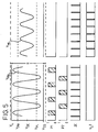
- FIG. 9 illustrates the problem caused.
- the composite voltage V M represents the voltage applied to the control circuit during a period of high range alternating input voltage.
- the composite voltage V M has positive peaks at times t p1 , t p2 , t p3 and negative peaks at times t' p1 , t' p2 .
- Both upper and lower peak detection thresholds, V TH , V TL are included, with optional additional thresholds V' TH , V' TL for hysteresis. Crossing of these thresholds by the voltage V M leads to the production of peak detection pulses P1, P2.
- the comparison signal CS changes state every time the composite voltage V M crosses the baseline crossing detection thresholds V ZC , V' ZC .
- a drop ⁇ V C in voltage V C occurs at time t ⁇ .
- V M monitored by the automatic voltage sensitive switch control circuit 30 includes a DC offset voltage V DC equal to 1 ⁇ 2V C , V M drops by 1 ⁇ 2 ⁇ V C . Due to this, the positive peak voltage occurring at time t p2 does not cross V TH , the positive peak detection threshold. No peak detection pulse is therefore present on signal P1; a peak of high voltage input goes un-detected.
- the thresholds V TL , V' TL are crossed early and late, respectively, causing a longer than usual pulse on signal P2.
- the voltage V C has not fully recovered by the time t p3 the next positive peak occurs, and hence the peak detection pulse on signal P1 is of reduced width, and its rising and falling edges are out of phase with those of other cycles. Similarly, during this period of reduced V C , the baseline crossing points, detected by the crossing of voltages V ZC , V' ZC are out of phase with those of other cycles, and do not correspond to the location at which the mains input voltage actually crosses the zero voltage level.
- FIG 10 shows another consequence of the independence of the reference voltages from the circuit supply voltage defined by V C .
- V M is the composite voltage supplied to the control circuit while a low range alternating input voltage is present. Neither of the peak detection signals P1 and P2 produce pulses, as the signal V M never exceeds V TH or V TL .
- the automatic doubler/bridge circuit is in voltage doubling rectification mode. However, as in figure 9, at time t ⁇ the voltage V C drops by an amount ⁇ V C . As discussed above, the magnitude of V M reduces, and at the negative peak at time t' p2 , the lower threshold V TL is crossed, and signal P2 produces a pulse, indicating a high range voltage. This will immediately stop voltage doubling mode, causing a temporary reduction in the output voltage of the rectifier circuit. Analogous problems may be encountered during a temporary increase in the value of V C , and hence V DC . Such behaviour is unacceptable for system level performance.
- a voltage reference circuit will be discussed, wherein the reference voltages are affected by variations in the magnitude of the power supply voltage V C , such that there is always a fixed voltage between each of them and the DC component V DC of the composite voltage V M .
- V DC the DC offset of the composite voltage V M .
- this voltage may be 1 ⁇ 2V C .
- the DC component could, however, be any fraction of V C , chosen such that the whole possible range of V M lies within the appropriate permitted range.
- V M 1 ⁇ 2.V C + n .
- V LN n is a fraction suitably chosen such the whole range of V M lies within the range between the nominal values of V 4 and V ss , for the highest expected value of V LN .
- each reference voltage may be detected by detecting the crossing of certain reference voltages corresponding to values of n .V LN .
- each reference voltage is tracking the DC offset voltage V DC , plus a certain fixed voltage V p which is the required certain value of n .V LN .
- V p the required reference voltages are obtained.
- These reference voltages will then vary in magnitude exactly as the DC offset voltage V DC varies.
- Both the DC offset voltage V DC and the certain fixed voltage V p are referenced to the ground voltage V ss .
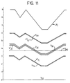
- Figure 11 shows the required function of the voltage reference circuit. All necessary reference voltages, V TH , V' TH , V ZC , V' ZC , V' TL , V TL track variations in 1 ⁇ 2V C , in this example, or any other value that V DC may take. As the voltage V C varies, the values of all the reference voltages vary, keeping a constant difference between each reference voltage and V DC . Voltage reference sources such as the amplified bandgap reference discussed above will supply a voltage x .V BG , constant with respect to the ground voltage V ss . This, however, varies in magnitude when considered with respect to V DC .
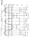
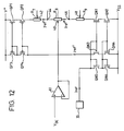
- FIG. 12 shows a circuit embodying such a voltage reference.
- a buffer amplifier A1 receives the DC offset voltage V DC , and supplies it to node 40, at the centre of a resistive divider network comprising resistors R 7 , R 8 , R 9 .
- Several nodes 42, 44, 46, 48 are tapped from this resistive divider network.
- This network is connected in series, and forms a first circuit branch, with two p-channel MOS transistors QP1, QP2 in series, connected also to the positive-most supply voltage V 4 , and two n-channel MOS transistors in series QN1, QN2, also connected to a ground voltage V ss .
- a second, parallel, circuit branch has two p-channel MOS transistors QP3, QP4 and two n-channel transistors QN3, QN4 in series respectively between V 4 and V ss .
- the p-channel transistors QP3, QP4 have their gates connected to the gates of transistors QP1, QP2 respectively, and to their own source terminals.
- the n-channel transistors QN3, QN4 have their gates connected to the gates of transistors QN1, QN2, respectively.
- a third parallel circuit branch comprises two n-channel MOS transistors QN5, QN6 connected in series, the source of QN6 being connected to the ground voltage V ss , the drain of QN5 being connected to the output of a constant current generator IG, which generates a constant current Iref through the transistors QN5, QN6.
- the gates of transistors QN5 and QN6 are connected to the gates of transistors QN3, QN4 respectively, and also to their own respective drain terminals.
- the constant current generator IG passes its reference current Iref through the two n-channel transistors QN5, QN6. These are each connected as a current mirror with transistors QN3, QN4 respectively. An identical current, Iref', therefore flows through the second circuit branch.
- This second circuit branch consists of four transistors QP3, QP4, QN3, QN4, each connected as a current mirror with a corresponding transistor in the first circuit branch.
- the first circuit branch comprises an upper portion, including transistors QP1, QP2, and resistors R7, R8 as far as node 40; and a lower portion comprising the rest of the branch, that is resistors R9, R8 from node 40, and transistors QN1, QN2.
- the current mirrors comprising transistors QP3, QP1, QP4, QP2 cause a current Iref'', equal to Iref, to flow in the upper part of the first circuit branch.
- the current mirrors comprising transistors QN3, QN1, QN4, QN2 cause a current Iref''', equal to Iref, to flow in the lower portion of the first circuit branch.
- the output of the buffer amplifier A1 holds the voltage V DC at node 40.
- the voltages at each of the nodes 42, 44, 46, 48 are then accurately held at voltages V DC ⁇ Iref.Rt, where Rt is the total resistance between the node in question and node 40.
- resistors R 7 , R 8 , R 9 all of which may be adjustable, accurate reference voltages are available for any desired value, with respect to the DC component V DC .
- the difference between the voltage at each node and node 40 is fixed by the constant current source output Iref, and the adjustments and values of resistors R 7 , R 8 , R 9 . If only voltages greater than V DC or only voltages less than V DC were required, resistors would only be necessary in either the upper or the lower portions of the first circuit branch.
- this circuit can provide the required voltage references of V DC ⁇ V p , it suffers from variations in the absolute value of the resistors, when implemented in integrated form, together with variations of resistance with temperature.
- the current source IG and the transistors may suffer from matching errors and tolerance deviations.
- FIG. 13 shows a second circuit for a voltage reference capable of the required functionality, which does not suffer from the above limitations.
- a bandgap voltage reference BG is supplied by the two available power supply voltages, V 4 , V ss which have a difference of V C . Its output voltage V BG is applied to the input of buffer amplifier A2, whose output will also be at voltage V BG .
- a resistive divider network comprising resistors R 10 , R 12 provides a DC voltage V i to a non-inverting input of an opamp A3.
- An inverting input of opamp A3 is connected to the output of the buffer amplifier A2, via a resistor R 13 .
- a feedback resistor R 14 is connected between the output V o and the inverting input of the operational amplifier A3. As is normal with operational amplifiers, the inverting terminal will be at the same voltage as the non-inverting input.
- the output voltage V BG of the voltage reference BG is at a fixed value with respect to the voltage V ss , and is independent of any fluctuations in the supply voltage V C .
- V i is a fraction of V 4 with respect to V ss and therefore proportionately follows any variation in the supply voltage V C .
- the V i term is the DC offset term which must correspond to V DC
- the V BG term corresponds to the fixed voltage V p .
- the operational amplifier A3 thus performs both multiplication of V BG by (R 14 /R 13 ) to obtain the fixed voltage V p and offsets V p by the voltage V DC .
- V DC 1 ⁇ 2V C
- V i (1 + R 14 /R 13 ) 1 ⁇ 2V C
- V i 1 ⁇ 2V C .R 13 /(R 13 + R 14 ).
- V i is directly proportional to V C , and provides a component of 1 ⁇ 2V C at the output of amplifier A3, any variation ⁇ V C of the voltage V C will be reflected with a variation of 1 ⁇ 2 ⁇ V C at the output of amplifier A3.
- the V BG element remains unaffected by the variation in V C , providing the required reference voltage V BG , with reference to V ss .
- the output voltage of amplifier A3 is therefore at a voltage V p less than V C .
- the voltage V p never changes, whatever variation occur in V C , provided that a minimum voltage is maintained, as required to ensure correct operation of the voltage reference BG. This minimum voltage may be around 41 ⁇ 2V.
- the output of amplifier A3 therefore fulfills the function of providing a voltage reference which varies with V DC , but which maintains a fixed value with respect to V DC , independent of variations of V C .
- This circuit allows the generation of any voltage below V DC .
- an inverting buffer amplifier is used.
- Figure 13A shows an inverting buffer amplifier, used to provide the threshold voltages above V BG .
- An operational amplifier A4 has a non-inverting input connected to V DC , which may be set by a resistive divider between the power supplies.
- Equal resistances R 15 , R 16 are connected between the inverting output and an output of amplifier A4, and the inverting input of amplifier A4 and the output of amplifier A3, figure 13, respectively.
- a resistive divider may be set up between the outputs of A3 and A4, to supply each of the required reference voltages. This may advantageously combined with the function of resistors R 15 , R 16 .
- Figure 13B shows a circuit allowing all required threshold voltages, V TH , V' TH , V' ZC , V ZC , V' TL , V TL , to be obtained from the two peak detection threshold values V TH , V TL .
- Circuit elements which are identical to those of figures 13 and 13A have identical reference symbols.
- a first resistive divider comprising resistors R 17 , node 50, resistor R 18 , node 52 and resistor R 12 is connected between the supply V 4 and ground V ss .
- a second resistive divider network comprising: resistor R 19 ; node 54; resistor R 20 ; node 56; resistor R 21 ; node 58; resistor R 22 ; node 60; resistor R 23 ; node 62 and resistor R 24 is connected between the outputs of amplifiers A3, A4 respectively.
- each pair of reference voltages (V TH and V TL ; V' TH and V' TL at nodes 62, 54; V' Z and V Z at nodes 56, 60) are symmetrical about V DC , and the voltage at node 58 is equal to the DC component V DC , as required for proper biasing of amplifier A4.
- Resistors R 19 , R 20 , R 21 together perform the function of R 15 in figure 13A, and resistors R 22 , R 23 , R 24 perform the function of R 16 in figure 13A.
- Each of the reference voltages described is then connected to a respective voltage comparator to allow peak and zero crossing detection to be carried out, as described above.
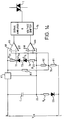
- Figure 14 shows a third embodiment of a DC voltage supply circuit according to the invention, using discrete components. Again, features similar to those in figure 8 have similar reference numbers.
- a half-wave rectifier comprises diode D 5 , resistor R 4 , node 22 and capacitor C, respectively connected in series between the live line L and the neutral line N.
- a three terminal regulator X1 has: a ground input connected to node 22; a voltage input connected to the neutral line N; and a voltage output connected a node 68.
- Two resistors R 1 , R 2 are connected in series between between the live line L and node 22 respectively. The two resistors share a common node 70.
- a further resistor R 3 is connected between the node 68 and the node 70.
- a resistor R Z1 , a node 72, zener diode Z TH , node 73, zener diode Z TL , node 74 and resistor R Z2 are respectively connected in series between node 68 and node 22.
- Two comparators A5, A6 have power supply connections connected to nodes 68 and 22.
- a non-inverting input of A5 is connected to node 70, as is an inverting input of A6.
- An inverting input of A5 is connected to node 72, and a non-inverting input of A6 is connected to node 74.
- a signal amplifier and voltage shifter 76 has two inputs each connected to an output of A5 and A6.
- the signal amplifier and voltage shifter 76 has an output connected to a gate input of triac T.
- the zener diodes Z TL , Z TH set the low and high peak detection thresholds V TL and V TH , respectively.
- Resistors R Z1 , R Z2 supply a zener diode bias current, and are chosen such that the node 73 between the zener diodes is at the DC offset voltage V DC .
- Nodes 72 and 74 are then held at voltages greater and less than V DC , respectively, by voltages equal to the breakdown voltages of the zener diodes Z TH , Z TL , respectively.
- the comparators A5, A6 each produce a high output when the voltage at node 70 exceeds the voltage at node 72, or falls below the voltage of node 74, respectively.
- the voltage at node 70 is a composite voltage, as discussed for other embodiments of the invention, being a scaled representation of the AC input voltage, supplied by the series connection of R 1 , R 2 , added to a DC offset voltage V DC provided by a DC current supplied by R 3 , through R 2 .
- the diode D 5 , resistor R 4 and capacitor C function as described for other embodiments of the invention, to provide a DC voltage across capacitor C.
- This DC voltage is regulated by X1, to fix V ss , node 22, at a fixed voltage, for example 9V, less than the neutral line N voltage.
- the AC input voltage V LN is hence scaled down and voltage shifted, allowing detection of both high and low peaks, gaining the advantages described of full-wave voltage sensing, in an embodiment using discrete components.
- the signal amplifier and voltage shifter 76 produces gate pulses to the triac, T when no output pulses are produced by A5, A6, - indicating a low-range AC input voltage, and so enabling voltage doubling rectification mode of an associated doubler/bridge rectifier - and suppresses such gate pulses when output pulses from A5, A6 are present - indicating a high-range AC input voltage, and so ensuring that bridge rectification mode is used.
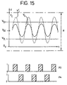
- Figure 15 shows the voltages V I , V I ' at node 70, for low-range and high-range AC input voltages, respectively.
- the scaled AC input voltage is shifted by DC offset V DC , and compared with the upper and lower thresholds V TH , V TL .
- the outputs P3, P4 of comparators A5, A6, respectively, correspond to a high voltage input V I '.
- R denotes the allowed range of input voltages to the control circuit.
- Zener diode breakdown voltages have a tolerance of around ⁇ 10%, and so may provide less accurate peak voltage detection than other embodiments described.
- circuits of the invention may equally be used with input AC voltages with non-zero baseline levels, with suitable adjustment of resistor values and voltage threshold levels.
Landscapes
- Engineering & Computer Science (AREA)
- Microelectronics & Electronic Packaging (AREA)
- Physics & Mathematics (AREA)
- Nonlinear Science (AREA)
- Electromagnetism (AREA)
- General Physics & Mathematics (AREA)
- Radar, Positioning & Navigation (AREA)
- Automation & Control Theory (AREA)
- Power Engineering (AREA)
- Rectifiers (AREA)
- Control Of Voltage And Current In General (AREA)
- Measurement Of Current Or Voltage (AREA)
Applications Claiming Priority (3)
| Application Number | Priority Date | Filing Date | Title |
|---|---|---|---|
| GB939314262A GB9314262D0 (en) | 1993-07-09 | 1993-07-09 | A multistandard ac/dc converter embodying mains voltage detection |
| GB9314262 | 1993-07-09 | ||
| EP94304903A EP0633652B1 (de) | 1993-07-09 | 1994-07-04 | Gleichspannungsversorgungsschaltung |
Related Parent Applications (2)
| Application Number | Title | Priority Date | Filing Date |
|---|---|---|---|
| EP94304903A Division EP0633652B1 (de) | 1993-07-09 | 1994-07-04 | Gleichspannungsversorgungsschaltung |
| EP94304903.1 Division | 1994-07-04 |
Publications (1)
| Publication Number | Publication Date |
|---|---|
| EP0794477A1 true EP0794477A1 (de) | 1997-09-10 |
Family
ID=10738568
Family Applications (2)
| Application Number | Title | Priority Date | Filing Date |
|---|---|---|---|
| EP94304903A Expired - Lifetime EP0633652B1 (de) | 1993-07-09 | 1994-07-04 | Gleichspannungsversorgungsschaltung |
| EP97106656A Withdrawn EP0794477A1 (de) | 1993-07-09 | 1994-07-04 | Schaltung zur Spannungserzeugung |
Family Applications Before (1)
| Application Number | Title | Priority Date | Filing Date |
|---|---|---|---|
| EP94304903A Expired - Lifetime EP0633652B1 (de) | 1993-07-09 | 1994-07-04 | Gleichspannungsversorgungsschaltung |
Country Status (6)
| Country | Link |
|---|---|
| US (2) | US5572415A (de) |
| EP (2) | EP0633652B1 (de) |
| JP (1) | JP2913574B2 (de) |
| DE (1) | DE69415422T2 (de) |
| GB (1) | GB9314262D0 (de) |
| SG (2) | SG46395A1 (de) |
Cited By (1)
| Publication number | Priority date | Publication date | Assignee | Title |
|---|---|---|---|---|
| EP0913755A3 (de) * | 1997-10-30 | 1999-05-19 | Xerox Corporation | Spannungswandler |
Families Citing this family (35)
| Publication number | Priority date | Publication date | Assignee | Title |
|---|---|---|---|---|
| US5703476A (en) * | 1995-06-30 | 1997-12-30 | Sgs-Thomson Microelectronics, S.R.L. | Reference voltage generator, having a double slope temperature characteristic, for a voltage regulator of an automotive alternator |
| US5793626A (en) * | 1996-05-29 | 1998-08-11 | Lucent Technologies Inc. | High efficiency bimodal power converter and method of operation thereof |
| US5686823A (en) * | 1996-08-07 | 1997-11-11 | National Semiconductor Corporation | Bandgap voltage reference circuit |
| JP3531385B2 (ja) * | 1996-10-28 | 2004-05-31 | ソニー株式会社 | 電源装置 |
| US6212083B1 (en) * | 1997-05-20 | 2001-04-03 | Daikin Industries, Ltd. | Single-phase rectifier |
| US5796244A (en) * | 1997-07-11 | 1998-08-18 | Vanguard International Semiconductor Corporation | Bandgap reference circuit |
| US6137700A (en) * | 1997-10-08 | 2000-10-24 | Daikin Industries, Ltd. | Converter with a high power factor using a DC center point voltage |
| US5877615A (en) * | 1997-11-06 | 1999-03-02 | Utek Semiconductor Corporation | Dynamic input reference voltage adjuster |
| US5886892A (en) * | 1997-12-05 | 1999-03-23 | Hewlett-Packard Company | Power supply with improved inrush circuit for limiting inrush current |
| US6204723B1 (en) | 1999-04-29 | 2001-03-20 | International Business Machines Corporation | Bias circuit for series connected decoupling capacitors |
| KR20010001187A (ko) * | 1999-06-02 | 2001-01-05 | 구자홍 | 자동 전압 전환장치 |
| JP2002078343A (ja) * | 2000-08-30 | 2002-03-15 | Brother Ind Ltd | ノイズ除去回路 |
| US6384586B1 (en) * | 2000-12-08 | 2002-05-07 | Nec Electronics, Inc. | Regulated low-voltage generation circuit |
| US7177610B2 (en) * | 2001-01-12 | 2007-02-13 | Silicon Laboratories Inc. | Calibrated low-noise current and voltage references and associated methods |
| US6388906B1 (en) * | 2001-04-20 | 2002-05-14 | Bogen Communications, Inc. | Backslope regulator system |
| US6603645B2 (en) * | 2001-12-20 | 2003-08-05 | Taiwan Semiconductor Manufacturing Co., Ltd. | Source line high voltage driver circuit with improved reliability and read performance |
| JP2004048897A (ja) * | 2002-07-11 | 2004-02-12 | Shimano Inc | 自転車用ダイナモの充電装置 |
| JP4596866B2 (ja) * | 2003-09-09 | 2010-12-15 | パナソニック株式会社 | モータ駆動装置 |
| US7362599B2 (en) * | 2004-12-13 | 2008-04-22 | Thomas & Betts International, Inc. | Switching power supply with capacitor input for a wide range of AC input voltages |
| KR100700787B1 (ko) * | 2005-08-16 | 2007-03-27 | 엘지전자 주식회사 | 영상표시기기의 전원 제어장치 |
| US7663928B2 (en) * | 2007-10-09 | 2010-02-16 | Ememory Technology Inc. | Sense amplifier circuit having current mirror architecture |
| JP2015039087A (ja) * | 2011-12-20 | 2015-02-26 | 株式会社村田製作所 | 半導体集積回路装置および高周波電力増幅器モジュール |
| WO2014085266A1 (en) * | 2012-11-30 | 2014-06-05 | Intel Corporation | Apparatus, method and system for determining reference voltages for a memory |
| WO2015056341A1 (ja) * | 2013-10-18 | 2015-04-23 | 三菱電機株式会社 | 直流電源装置、電動機駆動装置、空気調和機および冷蔵庫 |
| JP6504832B2 (ja) | 2014-01-28 | 2019-04-24 | ゼネラル・エレクトリック・カンパニイ | 統合された取り付けおよび冷却の装置、電子装置、および車両 |
| DE112015000898A5 (de) | 2014-02-21 | 2016-12-01 | Brusa Elektronik Ag | Ladeschaltung für einen Akkumulator mit erhöhter Ausgangsspannung |
| EP2911264A1 (de) * | 2014-02-21 | 2015-08-26 | Brusa Elektronik AG | Ladeschaltung für einen Akkumulator mit erhöhter Ausgangsspannung |
| US9826582B2 (en) | 2014-06-15 | 2017-11-21 | Lunera Lighting, Inc. | LED retrofit lamp with a strike barrier |
| US9686828B2 (en) * | 2014-06-15 | 2017-06-20 | Lunera Lighting, Inc. | LED retrofit lamp with a strike barrier |
| US10073512B2 (en) | 2014-11-19 | 2018-09-11 | General Electric Company | System and method for full range control of dual active bridge |
| FR3034924A1 (fr) * | 2015-04-07 | 2016-10-14 | St Microelectronics Tours Sas | Convertisseur alternatif-continu a limitation du courant d'appel |
| FR3034926A1 (fr) | 2015-04-07 | 2016-10-14 | St Microelectronics Tours Sas | Convertisseur de puissance a limitation du courant d'appel |
| US10436856B2 (en) * | 2015-12-24 | 2019-10-08 | Asahi Kasei Microdevices Corporation | Magnetic sensor apparatus and current sensor apparatus |
| US10116233B2 (en) * | 2017-02-14 | 2018-10-30 | Yang Chen | Hybrid full bridge-voltage doubler rectifier and single stage LLC converter thereof |
| GB2618371A (en) * | 2022-05-05 | 2023-11-08 | Tdk Lambda Uk Ltd | Switch controller circuit and method for controlling switching |
Citations (3)
| Publication number | Priority date | Publication date | Assignee | Title |
|---|---|---|---|---|
| US4007415A (en) * | 1974-12-26 | 1977-02-08 | Nippon Kogaku K.K. | Constant voltage generating circuit |
| DE1937714B2 (de) * | 1969-07-21 | 1977-06-02 | Texaco Development Corp., New York, N.Y. (V.St.A.) | Schaltungsanordnung zum stabilisieren von gleichspannung |
| WO1991007713A1 (en) * | 1989-11-13 | 1991-05-30 | British Technology Group Ltd | Transducer power supply |
Family Cites Families (22)
| Publication number | Priority date | Publication date | Assignee | Title |
|---|---|---|---|---|
| GB1299560A (en) * | 1970-07-02 | 1972-12-13 | Rollei Werke Franke Heidecke | Power supply apparatus for electronic flash guns |
| US4260946A (en) * | 1979-03-22 | 1981-04-07 | Rca Corporation | Reference voltage circuit using nested diode means |
| US4268899A (en) * | 1979-06-15 | 1981-05-19 | Sperry Corporation | Bridge-doubler rectifier |
| DE3321903A1 (de) * | 1983-06-16 | 1984-12-20 | Siemens AG, 1000 Berlin und 8000 München | Schaltungsanordnung fuer elektrogeraete mit automatischer spannungswahl |
| JPS6025391U (ja) * | 1983-07-27 | 1985-02-21 | 日本ケミコン株式会社 | 電源装置 |
| DE3344105A1 (de) * | 1983-12-07 | 1985-06-27 | Deutsche Thomson-Brandt Gmbh, 7730 Villingen-Schwenningen | Netzgleichrichter fuer zwei verschieden hohe netzspannungen |
| US4590546A (en) * | 1984-02-23 | 1986-05-20 | Rca Corporation | Variable input voltage regulator circuit |
| US4665323A (en) * | 1984-10-25 | 1987-05-12 | Zenith Electronics Corporation | Electronically switchable power source |
| EP0224488A1 (de) * | 1985-06-05 | 1987-06-10 | Caterpillar Inc. | Analog-zu-tastverhältnis-umsetzer |
| JP2628642B2 (ja) * | 1987-03-27 | 1997-07-09 | 富士電気化学株式会社 | 自動電圧切替電源 |
| US4780805A (en) * | 1987-07-21 | 1988-10-25 | Ncr Corporation | Low/high input voltage power supply |
| US4876637A (en) * | 1988-03-22 | 1989-10-24 | Kabushiki Kaisha Toshiba | Power converter and method of controlling the same |
| US4864488A (en) * | 1988-06-27 | 1989-09-05 | Ncr Corporation | Single level D.C. output voltage power supply |
| DE3833400A1 (de) * | 1988-10-01 | 1990-04-05 | Lust Electronic Systeme Gmbh | Vorrichtung zur erzeugung einer geglaetteten gleichspannung aus einer wechsel- oder drehspannungsquelle sowie verfahren zur steuerung der relation zwischen der hoehe der wechsel- oder drehspannung und der hoehe der geglaetteten gleichspannung |
| JPH01274664A (ja) * | 1989-02-08 | 1989-11-02 | Fuji Electric Co Ltd | 直流定電圧電源装置 |
| US4933832A (en) * | 1989-06-12 | 1990-06-12 | Compaq Computer Corp. | Automatic line monitor |
| US4980812A (en) * | 1989-11-09 | 1990-12-25 | Exide Electronics | Uninterrupted power supply system having improved power factor correction circuit |
| FR2659179B1 (fr) * | 1990-03-05 | 1994-11-10 | Sgs Thomson Microelectronics | Redresseur susceptible de fonctionner avec au moins deux plages distinctes de tension alternative d'alimentation. |
| JP2634685B2 (ja) * | 1990-07-24 | 1997-07-30 | シャープ株式会社 | 半導体装置の電圧降下回路 |
| US5119283A (en) * | 1991-06-10 | 1992-06-02 | General Electric Company | High power factor, voltage-doubler rectifier |
| JPH0561558A (ja) * | 1991-08-30 | 1993-03-12 | Sharp Corp | 基準電圧発生回路 |
| US5287263A (en) * | 1992-07-01 | 1994-02-15 | Digital Equipment Corporation | Inrush current control circuit |
-
1993
- 1993-07-09 GB GB939314262A patent/GB9314262D0/en active Pending
-
1994
- 1994-07-04 EP EP94304903A patent/EP0633652B1/de not_active Expired - Lifetime
- 1994-07-04 DE DE69415422T patent/DE69415422T2/de not_active Expired - Fee Related
- 1994-07-04 EP EP97106656A patent/EP0794477A1/de not_active Withdrawn
- 1994-07-04 SG SG1996004238A patent/SG46395A1/en unknown
- 1994-07-04 SG SG1999000933A patent/SG78333A1/en unknown
- 1994-07-06 US US08/271,288 patent/US5572415A/en not_active Expired - Lifetime
- 1994-07-11 JP JP6158877A patent/JP2913574B2/ja not_active Expired - Fee Related
-
1996
- 1996-01-24 US US08/590,091 patent/US5612613A/en not_active Expired - Lifetime
Patent Citations (3)
| Publication number | Priority date | Publication date | Assignee | Title |
|---|---|---|---|---|
| DE1937714B2 (de) * | 1969-07-21 | 1977-06-02 | Texaco Development Corp., New York, N.Y. (V.St.A.) | Schaltungsanordnung zum stabilisieren von gleichspannung |
| US4007415A (en) * | 1974-12-26 | 1977-02-08 | Nippon Kogaku K.K. | Constant voltage generating circuit |
| WO1991007713A1 (en) * | 1989-11-13 | 1991-05-30 | British Technology Group Ltd | Transducer power supply |
Cited By (1)
| Publication number | Priority date | Publication date | Assignee | Title |
|---|---|---|---|---|
| EP0913755A3 (de) * | 1997-10-30 | 1999-05-19 | Xerox Corporation | Spannungswandler |
Also Published As
| Publication number | Publication date |
|---|---|
| EP0633652A2 (de) | 1995-01-11 |
| GB9314262D0 (en) | 1993-08-18 |
| EP0633652B1 (de) | 1998-12-23 |
| SG46395A1 (en) | 1998-02-20 |
| US5612613A (en) | 1997-03-18 |
| JPH07264862A (ja) | 1995-10-13 |
| JP2913574B2 (ja) | 1999-06-28 |
| EP0633652A3 (de) | 1995-04-19 |
| DE69415422D1 (de) | 1999-02-04 |
| SG78333A1 (en) | 2001-02-20 |
| DE69415422T2 (de) | 1999-06-24 |
| US5572415A (en) | 1996-11-05 |
Similar Documents
| Publication | Publication Date | Title |
|---|---|---|
| EP0633652B1 (de) | Gleichspannungsversorgungsschaltung | |
| EP1708069A1 (de) | Überstromerkennungsschaltung und regler damit | |
| KR0128731B1 (ko) | 차동 증폭기와 전류 감지 회로 및 직접 회로 | |
| EP0570148B1 (de) | Elektrostatisches Voltmeter mit integrierten Hochspannungs-Schaltungen | |
| US5481179A (en) | Voltage reference circuit with a common gate output stage | |
| US6445305B2 (en) | CMOS low battery voltage detector | |
| JP4630764B2 (ja) | ハイ側のスイッチにおいて正および負のピークインダクタ電流を損失無くセンスする方法及び装置 | |
| EP0636892A2 (de) | Elektrostatisches Voltmeter | |
| JPH02233007A (ja) | Mosトランジスタの電流を検出する装置及び方法 | |
| US6686789B2 (en) | Dynamic low power reference circuit | |
| JP2692940B2 (ja) | 固定基準電圧レベルの交流電圧によるクロスオーバを検出する回路配置 | |
| JP2000516338A (ja) | ソース側負荷を有する電力半導体構成素子の負荷電流を検出するための回路装置 | |
| US4488438A (en) | Square-wave current generator | |
| EP0670502B1 (de) | Messvorrichtung für eine elektrische Grösse | |
| US20050275414A1 (en) | Double-mirror short-circuit detection | |
| KR100259349B1 (ko) | 백바이어스 전압레벨 검출기 | |
| US4000410A (en) | Circuit arrangement for superposing starting conditions at an electrical operating means-simulator composed of RC-elements | |
| US10581431B2 (en) | Self capacitance drive offset cancellation in touch controller integrated circuits | |
| JP2015018313A (ja) | ホール素子駆動回路 | |
| JPWO2006057054A1 (ja) | 湿度計測装置 | |
| EP1732210A1 (de) | Pilotsignal-detektionsschaltung und diese schaltung enthaltende integrierte halbleiterschaltung | |
| JPH0229165B2 (de) | ||
| JP2949242B2 (ja) | コンデンサの絶縁抵抗測定装置 | |
| KR0163724B1 (ko) | 전압 레귤레이터 | |
| SU425168A1 (ru) | Прецизионный стабилизатор постоянного напряжения |
Legal Events
| Date | Code | Title | Description |
|---|---|---|---|
| PUAI | Public reference made under article 153(3) epc to a published international application that has entered the european phase |
Free format text: ORIGINAL CODE: 0009012 |
|
| AC | Divisional application: reference to earlier application |
Ref document number: 633652 Country of ref document: EP |
|
| AK | Designated contracting states |
Kind code of ref document: A1 Designated state(s): DE FR GB IT |
|
| 17P | Request for examination filed |
Effective date: 19980306 |
|
| 17Q | First examination report despatched |
Effective date: 20010808 |
|
| RAP1 | Party data changed (applicant data changed or rights of an application transferred) |
Owner name: STMICROELECTRONICS PTE LTD. |
|
| STAA | Information on the status of an ep patent application or granted ep patent |
Free format text: STATUS: THE APPLICATION IS DEEMED TO BE WITHDRAWN |
|
| 18D | Application deemed to be withdrawn |
Effective date: 20040203 |
|
| RIN1 | Information on inventor provided before grant (corrected) |
Inventor name: MOHAN, MUNI Inventor name: DUTT, SAIBUL |