EP0791948B1 - Elektrodenscheibe für Plasma-Ätzvorrichtung - Google Patents
Elektrodenscheibe für Plasma-Ätzvorrichtung Download PDFInfo
- Publication number
- EP0791948B1 EP0791948B1 EP97102246A EP97102246A EP0791948B1 EP 0791948 B1 EP0791948 B1 EP 0791948B1 EP 97102246 A EP97102246 A EP 97102246A EP 97102246 A EP97102246 A EP 97102246A EP 0791948 B1 EP0791948 B1 EP 0791948B1
- Authority
- EP
- European Patent Office
- Prior art keywords
- plasma
- etching
- electrode plate
- glassy carbon
- electrode
- Prior art date
- Legal status (The legal status is an assumption and is not a legal conclusion. Google has not performed a legal analysis and makes no representation as to the accuracy of the status listed.)
- Expired - Lifetime
Links
Images

Classifications
-
- H—ELECTRICITY
- H01—ELECTRIC ELEMENTS
- H01J—ELECTRIC DISCHARGE TUBES OR DISCHARGE LAMPS
- H01J37/00—Discharge tubes with provision for introducing objects or material to be exposed to the discharge, e.g. for the purpose of examination or processing thereof
- H01J37/32—Gas-filled discharge tubes
- H01J37/32009—Arrangements for generation of plasma specially adapted for examination or treatment of objects, e.g. plasma sources
-
- H—ELECTRICITY
- H10—SEMICONDUCTOR DEVICES; ELECTRIC SOLID-STATE DEVICES NOT OTHERWISE PROVIDED FOR
- H10P—GENERIC PROCESSES OR APPARATUS FOR THE MANUFACTURE OR TREATMENT OF DEVICES COVERED BY CLASS H10
- H10P50/00—Etching of wafers, substrates or parts of devices
-
- H—ELECTRICITY
- H01—ELECTRIC ELEMENTS
- H01J—ELECTRIC DISCHARGE TUBES OR DISCHARGE LAMPS
- H01J37/00—Discharge tubes with provision for introducing objects or material to be exposed to the discharge, e.g. for the purpose of examination or processing thereof
- H01J37/32—Gas-filled discharge tubes
- H01J37/32431—Constructional details of the reactor
- H01J37/32532—Electrodes
- H01J37/3255—Material
-
- Y—GENERAL TAGGING OF NEW TECHNOLOGICAL DEVELOPMENTS; GENERAL TAGGING OF CROSS-SECTIONAL TECHNOLOGIES SPANNING OVER SEVERAL SECTIONS OF THE IPC; TECHNICAL SUBJECTS COVERED BY FORMER USPC CROSS-REFERENCE ART COLLECTIONS [XRACs] AND DIGESTS
- Y10—TECHNICAL SUBJECTS COVERED BY FORMER USPC
- Y10S—TECHNICAL SUBJECTS COVERED BY FORMER USPC CROSS-REFERENCE ART COLLECTIONS [XRACs] AND DIGESTS
- Y10S156/00—Adhesive bonding and miscellaneous chemical manufacture
- Y10S156/914—Differential etching apparatus including particular materials of construction
Definitions
- the present invention relates to a plasma etching electrode plate of glassy carbon having a thickness grater than 4,5 mm, a thermal conductivity greater than 5 W/mK at 300 K and a carbon yield higher than 20 %.
- US-A-5074456 discloses a composite electrode for plasma etching processes in a parallel type plasma reactor.
- the upper electrode must meet a number of requirements in order to achieve the desired performance characteristics.
- the electrode must have defined electrical properties, such as impedance, current capacity and must be able to resist prolonged exposure to the generated plasma.
- the upper electrode must have chemical stability and should not generate large particles or large quantities of particles.
- the electrode material must have a high purity and should not release heavy metals or other contaminants into the zone between the opposed electrodes.
- An improved upper electrode construction is proposed using all types of electrode material such as polycrystalline silicon, graphite, aluminium, flame sprayed silicon powder and aluminium, quarz, zirconium; diamond coated materials and titanium oxides.
- a plasma etching electrode plate of glassy carbon having a thickness greater than 4,5 mm is disclosed. Usually, however, it was suggested to minimize the thickness of the electrode plate on economical reason.
- EP-A-0573915 discloses an electrode plate for use in plasma etching comprising a glassy carbon material having a bulk density of 1,5 to 1,57 g/cm 3 .
- the electrode material undertakes a heat treatment at the following stages: curring 200°C, carbonizing 1000°C, purification 2300°C.
- the resulting material has good mechanical properties (bending strength, shore hardness, porosity, density and durability) according to the low porosity of the cured polycarbodiimide resin.
- the disclosed apparatus is provided with paired parallel plate electrodes facing each other. One of them is located at the lower part of the chamber so that wafers (substrates) are placed on it. Another of them is located at the upper part of the chamber and has a number of small through holes for gas introduction. For etching, this apparatus applies a high-frequency electric power across the electrodes to induce discharge while introducing a reactive gas (such as halogen gas and freon gas) through the upper electrode. The resulting gas plasma attacks that part of the substrate which is not protected by the photoresist. In this way accurate fine circuit patterns are formed on the semiconductor wafer.
- a reactive gas such as halogen gas and freon gas
- the upper electrode for plasma etching is a disk having a number of small through holes as shown in Lee Chen's patent (Fig. 2) or Mark's patent (Fig. 3A). It varies in the shape, number, and arrangement of small holes depending on the apparatus and etching conditions. (In other words, not all electrodes of the same type can be used in common for any apparatus.) The shape of small holes strictly depends on the kind of the electrode for individual apparatus.
- Electrode plates made of glassy carbon have come into general use recently.
- Glassy carbon is a hard, macroscopically non-porous carbonaceous substance obtained by carbonization of a thermosetting resin. It is characterized by high strength, chemical inertness, gas impermeability, self-lubrication, toughness, and purity. Its another advantage over other materials is the least likely possibility of fine particles releasing themselves from the structure to contaminate the wafer during plasma etching.
- the ever-increasing degree of integration needs plasma-etching electrodes to meet requirements for configuration as well as physical and chemical properties.
- the plasma-etching electrodes should be least liable to wafer contamination with particles and to wearing.
- Efforts have been made to improve the plasma-etching electrodes of glassy carbon.
- a common way to keep uniform the surface temperature of a thin electrode plate is to tightly attach a cooling metal plate to the back of the electrode plate.
- a problem in this case is with the warp of the electrode plate.
- Warp forms a small gap which prevents close contact between the electrode plate and the cooling metal plate, resulting in insufficient heat dissipation. Therefore, it is necessary to devise a method for minimizing warp.
- the electrode plate should preferably be thick rather than thin from the standpoint of durability. Good durability prolongs the interval between shutdowns for electrode replacement.
- the uniformity of etch rate is important for accurate etching in view of the fact that finer circuit patterns are necessary for semiconductor devices with a higher degree of integration and the wafer size has exceeded 8 inches and is expected to exceed 12 inches in near future. Nevertheless, no efforts have been made to improve the uniformity of etch rate from the material viewpoint of the glassy carbon constituting the electrode.
- the etch rate is governed mainly by the temperature of the reaction system. In the case of a thick electrode plate, it is important for the uniform etch rate to keep uniform the temperature distribution on the electrode surface.
- the thick electrode plate of glassy carbon proposed in Japanese Patent Laid-open Nos. 362062/1992 and 100365/1994 mentioned above has been found unsatisfactory for plasma etching.
- the present inventors thoroughly investigated the relation between the properties of the electrode plate and the etch rate. As the result, it was found that it is possible to keep uniform the temperature distribution on the electrode surface and hence to carry out uniform etching invariably, if the electrode plate is made of glassy carbon having a thermal conductivity greater than a specific value and has a thickness greater than a specific value. This finding led to the present invention.
- a plasma-etching electrode plate of glassy carbon which is characterized by a thickness greater than 4.5 mm and a thermal conductivity greater than 5 W/m ⁇ K at 300K.
- the plasma-etching electrode plate is thicker than 4.5 mm so that it has a uniform, stable temperature and also has a uniform temperature distribution on its surface exposed to plasma. These characteristic properties contribute to the uniform etch rate of semiconductor wafers.
- the plasma-etching electrode plate should be a flat disk of glassy carbon having a number of through holes, should have a bulk specific gravity greater than 1.53 g/cc (measured after polishing), and should have a thermal conductivity greater than 5 W/m ⁇ K at 300K.
- the plasma-etching electrode plate of the present invention is a glassy carbon plate of uniform structure which is obtained by baking (for carbonization) from a thermosetting resin having a carbon yield higher than 20%.
- the carbon yield means the amount of carbon content (in wt%) which remains after baking at 800-1000°C in a nonoxidizing atmosphere.) It should have a high purity specified by less than 5 ppm of total ash content, less than 2 ppm of metal impurities, and less than 30 ppm of total sulfur content. In addition, it should be as flat as possible. These requirements should be met to prevent the diffusion of impurities into wafers and the contamination of wafers with fine particles.
- the important physical properties required of the plasma-etching electrode plate are a thickness greater than 4.5 mm, a thermal conductivity greater than 5 W/m ⁇ K at 300K, and a bulk specific gravity greater than 1.53 g/cc.
- the thermal conductivity and thickness specified above mean that the glassy carbon plate conducts heat well and has a large heat capacity. Owing to these properties, the electrode plate has a uniform temperature distribution on its surface with a minimum of temperature fluctuation. This temperature uniformity contributes to the uniform etch rate. These effects are enhanced by the high bulk specific gravity. The high bulk specific gravity also contributes to the resistance to wear by plasma.
- the electrode plate of glassy carbon With a thermal conductivity lower than 5 W/m ⁇ K at 300K and a thickness smaller than 4.5 mm, the electrode plate of glassy carbon is liable to temperature fluctuation due to heat generation resulting from plasma etching. This aggravates the uniformity of etch rate.
- An advantage of the thick electrode plate of glassy carbon is a high heat capacity, which eliminates the problem with warp encountered in thin electrode plates. (Warp prevents the close contact of the cooling metal plate.) It is possible for the thermally conductive, thick electrode plate to effectively suppress the fluctuation of the surface temperature distribution and hence to realise the uniform etch rate.
- An additional advantage of the thick electrode plate is the capability of handling large wafers and the long life.
- the glassy carbon plate meeting the above-mentioned requirements can be produced from a resin composition by molding, curing, and baking (for carbonization) in a nonoxidizing atmosphere.
- the resin composition is composed of a phenolic resin (having a molecular weight higher than 100 and a gelling time of 5-60 minutes) and furan or a derivative thereof. It is a liquid having a viscosity of 1-100 poise and containing more than 50 wt% resin.
- the thick glassy carbon plate tends to vary in structure (such as crystallinity and density) across its thickness. In an extreme case, the variation in structure leads to cracking during heat treatment.
- a phenolic resin precondensate is prepared from purified phenol and formalin by condensation reaction. It has a molecular weight higher than 100 and a gelling time of 5-60 minutes. Then, it is mixed with furan or a derivative thereof. Thus there is obtained a binary resin composition having a yield of carbonization of 65-75%.
- the examples of the furan derivative include furfuryl alcohol, furfural, and methyl ester of furancarboxylic acid, which are miscible with phenolic resins. They may be used alone or in combination with one another.
- the mixing ratio of furan to phenolic resin should be established adequately so that the resulting composition has a viscosity of 1-100 poise and contains more than 50% resin.
- the resin composition is formed into a disk by casting, centrifugal molding, or injection so that the eventually obtained glassy carbon plate is thicker than 4.5 mm.
- the molded disk is cured by heating.
- Polycarbodiimide as the raw material may be obtained from a mixture or copolymer of aliphatic, alicyclic, or aromatic isocyanates, such as 2,4-tolylenediisocyanate, 2,6-tolylenediisocyanate, a mixture thereof, crude tolylenediisocyanate, xylenediieocyanate, m-phenylenediisocyanate, naphthylene-1,5-diisocyanate, 4,4'-biphenylenediisocyanate, and 3,3'-dimethoxy-4,4'-biphenylenediisocyanate. It may be prepared by the process disclosed in Japanese Patent Laid-open Nos. 61599/1986 and 299316/1990. The organic diisocyanate is reacted in the presence of a polymerization catalyst and the resulting product (with solvent removed) is formed and cured by heating.
- aromatic isocyanates such as 2,4-tolylenedi
- Curing should be carried under strictly controlled conditions. Uneven curing leads to uneven carbon crystallization across the thickness of the glassy carbon plate.
- the curing of a thermosetting resin is exothermic and curing proceeds faster in the outer layer than in the inner layer. Rapid heating to accelerate dewatering and drying causes the outer layer to solidify and densify faster-than the inner layer. The solid outer layer prevents the release of water or reaction gas which is formed in the molded disk by curing reaction.
- the heating temperature is necessary to raise the heating temperature at a rate lower than 10°C/h, preferably lower than 5°C/h, more preferably lower than 2°C/h.
- the maximum temperature should be kept for a while until curing is completed.
- the curing temperature varies depending on the resin composition, hardener, and formulation. It is usually in the range of 140-200°C (or 200-250°C for polycarbodiimide resin). Complete curing will take more than hours.
- the resin molded product After curing, the resin molded product is heated (for baking and carbonization) at 800°C or above in a furnace with a nonoxidizing atmosphere. In this way there is obtained a glassy carbon plate. Heating in this step should be uniform because the resin molded product has a low thermal conductivity and hence carbonization proceeds faster in the outer layer than in the inner layer. To ensure uniform heating and carbonization, it is necessary to raise the temperature slowly at a rate lower than 2°C/h.
- Glassy carbon is gas-impermeable and has a large number of extremely small pores therein because it is amorphous-unlike crystalline graphite. Rapid carbonization shuts them up in the glassy carbon, resulting in a low bulk specific gravity. In addition, such remaining pores produce the heat insulating effect and hence lower the heat capacity of the glassy carbon.
- the resin molded product is held between graphite plates under pressure, and the assembly is placed in a graphite crucible and baked (for carbonization) in a heating furnace at 800-2500°C, with the temperature in the furnace adequately controlled. In this way it is possible to produce several grades of glassy carbon plates which vary in thermal conductivity.
- the stage of vigorous decomposition, the stage of vigorous gas evolution, and the stage of structure change following carbonization.
- the effect concomitant to reducing the number of pores is the effective protection of the electrode against breakage and excessive consumption by wear during use.
- the result is uniform wear on the electrode surface and hence an improved etch rate.
- Another way to obtain the desired thick product is to incorporate the raw material with a carbonaceous material, an easily carbonizable organic compound, or a metallic element or compound capable of combining with water or gas evolved by reaction.
- the substance for this purpose should be a particulate one finer than 2 ⁇ m so as to avoid the problem with particles falling on the wafer that develops as the electrode consumption.
- the glassy carbon plate is purified further by heating at 1400°C or above in an electric furnace through which a halogen gas (such as chlorine) is passed according to need.
- a halogen gas such as chlorine
- the small through holes for gas introduction may be formed in the electrode plate in the stage of molding from a resin or after the step of carbonization.
- the size of hole should be determined in anticipation of shrinkage that occurs during baking.
- drilling may be accomplished by electro arc machining.
- the raw material that can be used in the examples is a phenolic resin, furan resin, polyamide resin, or polycarbodiimide resin, or a mixture thereof which has a carbon yield higher than 20%.
- a precondensate of phenolic resin was prepared from phenol (purified by distillation under reduced pressure) and formalin. It has the molecular weight and gelling time as shown in Table 1. This phenolic resin (100 pbw) was incorporated with furfuryl alcohol (30 pbw) to give a resin composition having a viscosity of 40 poise and containing 55% resin.
- the resin composition was cast into a polyethylene vat, deaerated under reduced pressure (10 Torr) in a vacuum desiccator, and heated in an electric oven up to 200°C at a rate of 4°C/h and kept at this temperature for 5 hours. In this way there was obtained a molded product in the form of plate.
- the molded product was held between two flat graphite plates (G347, from Tokai Carbon Co., Ltd.) 10 mm thick.
- the assembly was placed in a graphite crucible and baked (for carbonization) in an electric furnace with an argon atmosphere.
- Baking was carried out by raising the temperature at a rate of 1-4°C/h, with the pressure of argon atmosphere varied in the electric furnace. The heating stage was held stationary for 5 hours each at 350°C, 450°C, and 550°C. The baking temperature and the furnace pressure are shown in Table 1.
- the glassy carbon plate had through holes (0.5 mm in diameter) made by electro arc machining at equal intervals of 2 mm at its central part. Thus there was obtained the desired plasma-etching electrode plate.
- the physical properties of the plasma-etching electrode plate are shown in Table 2. Thermal conductivity was measured according to JIS R1611-1991. Specific heat capacity was measured by using high-purity ⁇ -alumina as the reference and blackened aluminum as the light receiving plate. Heat diffusion rate was measured by using high-purity copper as the reference. Bulk specific gravity was measured by the Archimedes method (weighing the object in a liquid) according to JIS Z8807-1987.
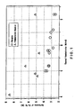
- Fig. 1 is a graph showing the relation between the thermal conductivity and the uniformity of etch rate after etching for 200 hours.
- Fig. 2 is a graph showing the relation between the thermal conductivity and the consumption of the electrode surface after etching for 200 hours. It is apparent that the samples meeting the requirements (a thermal conductivity higher than 5 W/m ⁇ K at 300K and a thickness larger than 4.5 mm) of the present invention are superior to the comparative samples in the uniformity of etch rate (even after etching for a long time) and the wear resistance of the electrode surface.
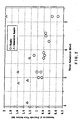
- Fig. 3 is a graph showing the relation between the bulk specific gravity and the consumption of the electrode surface after etching for 200 hours. It is apparent that the samples meeting the requirements (a bulk specific gravity higher than 1.53 g/cm 3 ) of the present invention are also superior in wear resistance as well as the uniformity of etch rate.
- the plasma-etching electrode plate of the present invention is a glassy carbon plate characterized by a thermal conductivity higher than a specific value at normal temperature and a thickness greater than a specific value. Owing to these characteristic properties, it permits etching on large semiconductor wafers at a uniform etch rate. In addition, it is capable of stable etching for a long time and has a greatly improved durability. Therefore, the present invention is of great industrial value.
- Example (Comparative Example) Variable factors Average molecular weight Celling time (min) Furnace pressure (Torr) Baking temperature (°C) 1 132 14 800 2000 2 132 14 1500 2000 3 132 14 800 2200 4 133 14 2000 2500 5 132 14 1500 2500 6 125 18 800 2000 7 125 18 800 2000 8 125 18 800 2500 9 125 18 2000 2000 10 125 18 2000 2500 11 125 18 800 1700 12 125 18 2000 1500 13 125 18 2000 1500 (1) 125 18 2000 1500 (2) 132 14 2000 2500 (3) 132 14 800 1400 (4) 125 18 800 2000 (5) 125 18 500 1700 (6) 125 18 800 1500 Table 2 Example (Comparative Example) Thermal conductivity (W/m ⁇ K) Thickness (mm) Bulk specific gravity (g/cc) Diameter (mm) Ratio of diameter to thickness 1 5.2 4.5 1.52 300 67 2 5.9 5.0 1.55 300 60 3 5.8 5.0 1.52 380 76 4 7.2 8.0 1.59 380 48 5 6.6
Landscapes
- Physics & Mathematics (AREA)
- Engineering & Computer Science (AREA)
- Plasma & Fusion (AREA)
- Chemical & Material Sciences (AREA)
- Analytical Chemistry (AREA)
- Drying Of Semiconductors (AREA)
- ing And Chemical Polishing (AREA)
- Carbon And Carbon Compounds (AREA)
- Ceramic Products (AREA)
Claims (3)
- Eine Elektroden-Platte zum Plasma-Ätzen aus Glaskohlenstoff mit einer Dicke größer als 4,5 mm, gekennzeichnet durch eine Wärmeleitfähigkeit größer als 5 W/mK bei 300K, erhalten durch Erhitzen zur Verkohlung eines hitzehärtenden Harzes, aufweisend einen Kohlenstoffgehalt von mehr als 20%.
- Eine Elektroden-Platte zum Plasma-Ätzen aus Glaskohlenstoff wie in Anspruch 1 definiert, welche gekennzeichnet ist durch eine spezifische Volumendichte von mehr als 1,53 g/cm3 (gemessen nach dem Polieren).
- Eine Elektroden-Platte zum Plasma-Ätzen aus Glaskohlenstoff, wie in einem der vorhergehenden Ansprüche definiert, welche ausgeformt wird aus einer hitzehärtenden Harz-Zusammensetzung, enthaltend ein oder mehrere hitzehärtende Harze und welche gebildet wird durch die Verkohlung eines ausgeformten Körpers aus der hitzehärtenden Harz-Zusammensetzung durch nachfolgendes Heizen des ausgeformten Körpers bei einer Temperatur von 300 bis 400 °C für mehr als 5 Stunden, 400 °C bis 500 °C für mehr als 5 Stunden und 500 °C bis 600 °C für mehr als 5 Stunden und Heizen des Körpers auf 800 °C bis 2500 °C, um die Verkohlung abzuschließen.
Applications Claiming Priority (3)
| Application Number | Priority Date | Filing Date | Title |
|---|---|---|---|
| JP52467/96 | 1996-02-15 | ||
| JP5246796 | 1996-02-15 | ||
| JP5246796 | 1996-02-15 |
Publications (3)
| Publication Number | Publication Date |
|---|---|
| EP0791948A2 EP0791948A2 (de) | 1997-08-27 |
| EP0791948A3 EP0791948A3 (de) | 1999-06-23 |
| EP0791948B1 true EP0791948B1 (de) | 2006-09-20 |
Family
ID=12915533
Family Applications (1)
| Application Number | Title | Priority Date | Filing Date |
|---|---|---|---|
| EP97102246A Expired - Lifetime EP0791948B1 (de) | 1996-02-15 | 1997-02-13 | Elektrodenscheibe für Plasma-Ätzvorrichtung |
Country Status (5)
| Country | Link |
|---|---|
| US (1) | US5993596A (de) |
| EP (1) | EP0791948B1 (de) |
| KR (1) | KR100427117B1 (de) |
| DE (1) | DE69736685T2 (de) |
| TW (1) | TW449820B (de) |
Families Citing this family (6)
| Publication number | Priority date | Publication date | Assignee | Title |
|---|---|---|---|---|
| JP2003533879A (ja) | 2000-05-12 | 2003-11-11 | 東京エレクトロン株式会社 | プラズマ処理システムにおける電極の厚さを調整する方法 |
| US20020127853A1 (en) * | 2000-12-29 | 2002-09-12 | Hubacek Jerome S. | Electrode for plasma processes and method for manufacture and use thereof |
| US6740403B2 (en) | 2001-04-02 | 2004-05-25 | Toyo Tanso Co., Ltd. | Graphitic polyhederal crystals in the form of nanotubes, whiskers and nanorods, methods for their production and uses thereof |
| JP3876167B2 (ja) * | 2002-02-13 | 2007-01-31 | 川崎マイクロエレクトロニクス株式会社 | 洗浄方法および半導体装置の製造方法 |
| US20040033361A1 (en) * | 2002-08-06 | 2004-02-19 | Kabushiki Kaisha Kobe Seiko Sho(Kobe Steel, Ltd.) | Component of glass-like carbon for CVD apparatus and process for production thereof |
| CN108984918B (zh) * | 2018-07-20 | 2023-04-18 | 辽宁石油化工大学 | 一种电渣重熔自耗电极熔化速率的预测方法 |
Family Cites Families (9)
| Publication number | Priority date | Publication date | Assignee | Title |
|---|---|---|---|---|
| JPH07114198B2 (ja) * | 1989-10-02 | 1995-12-06 | 東海カーボン株式会社 | プラズマエッチング用電極板 |
| JPH0814033B2 (ja) * | 1990-04-02 | 1996-02-14 | 東芝セラミックス株式会社 | プラズマエッチング用電極板 |
| US5074456A (en) * | 1990-09-18 | 1991-12-24 | Lam Research Corporation | Composite electrode for plasma processes |
| JP3252330B2 (ja) * | 1991-09-20 | 2002-02-04 | 東芝セラミックス株式会社 | プラズマエッチング用電極板 |
| JPH05208867A (ja) * | 1992-01-28 | 1993-08-20 | Tokai Carbon Co Ltd | 高耐食性ガラス状カーボン材 |
| JP2873988B2 (ja) * | 1992-05-25 | 1999-03-24 | 東海カーボン株式会社 | プラズマエッチング用電極板 |
| EP0573915A1 (de) * | 1992-06-12 | 1993-12-15 | Nisshinbo Industries, Inc. | Elektrodenplatte und Schablone zur Verwendung in Plasma-Ätzverfahren |
| JP3242166B2 (ja) * | 1992-11-19 | 2001-12-25 | 株式会社日立製作所 | エッチング装置 |
| JPH0941166A (ja) * | 1995-07-31 | 1997-02-10 | Kobe Steel Ltd | エッチング用電極、及びその製造方法 |
-
1997
- 1997-02-12 TW TW086101568A patent/TW449820B/zh not_active IP Right Cessation
- 1997-02-13 DE DE69736685T patent/DE69736685T2/de not_active Expired - Fee Related
- 1997-02-13 EP EP97102246A patent/EP0791948B1/de not_active Expired - Lifetime
- 1997-02-14 KR KR1019970004439A patent/KR100427117B1/ko not_active Expired - Fee Related
- 1997-02-14 US US08/799,957 patent/US5993596A/en not_active Expired - Lifetime
Also Published As
| Publication number | Publication date |
|---|---|
| KR970063561A (ko) | 1997-09-12 |
| EP0791948A2 (de) | 1997-08-27 |
| DE69736685D1 (de) | 2006-11-02 |
| DE69736685T2 (de) | 2007-10-04 |
| KR100427117B1 (ko) | 2004-09-04 |
| US5993596A (en) | 1999-11-30 |
| EP0791948A3 (de) | 1999-06-23 |
| TW449820B (en) | 2001-08-11 |
Similar Documents
| Publication | Publication Date | Title |
|---|---|---|
| EP1081749B1 (de) | Schutzelement für die innere oberfläche einer kammer und plasmabehandlungsvorrichtung | |
| US4264803A (en) | Resistance-heated pyrolytic boron nitride coated graphite boat for metal vaporization | |
| EP0219933B1 (de) | Siliziumcarbidsinterkörper mit hohem elektrischem Widerstand | |
| EP0791948B1 (de) | Elektrodenscheibe für Plasma-Ätzvorrichtung | |
| US6187704B1 (en) | Process for making heater member | |
| US5853523A (en) | Plasma-etching electrode plate | |
| KR100476350B1 (ko) | 플라즈마처리장치용전극판의제조방법 | |
| KR100361067B1 (ko) | 염소계 가스에 대한 내식성 부재 | |
| JPH06128762A (ja) | プラズマエッチング用電極板 | |
| EP0757374A1 (de) | Ätzelektrode und Herstellungsverfahren derselben | |
| JP3461120B2 (ja) | プラズマエッチング用電極板及びプラズマエッチング装置 | |
| JPH03119723A (ja) | プラズマエッチング用電極板 | |
| JP3255586B2 (ja) | プラズマエッチング用電極板 | |
| JP3349282B2 (ja) | プラズマエッチング用電極板 | |
| JP2003023002A (ja) | チャンバー内壁保護部材及びプラズマ処理装置 | |
| JP3465838B2 (ja) | プラズマエッチング用電極板 | |
| JP2002151483A (ja) | プラズマエッチング装置 | |
| JPH10291813A (ja) | プラズマエッチング用電極板 | |
| EP0803485A2 (de) | Verfahren zur Herstellung von Formkörpern aus Siliciumcarbid | |
| JPH0288467A (ja) | 窒化アルミニウム焼結体およびその製造方法 | |
| JP3736887B2 (ja) | プラズマエッチング用電極板 | |
| JP2000103677A (ja) | 半導体熱処理用シリコン含浸炭化珪素質材料及びその製造方法 | |
| JP2517392B2 (ja) | プラズマエッチング用電極板 | |
| JP3114604B2 (ja) | イオン注入装置用部品 | |
| JP3514336B2 (ja) | プラズマエッチング用電極板 |
Legal Events
| Date | Code | Title | Description |
|---|---|---|---|
| PUAI | Public reference made under article 153(3) epc to a published international application that has entered the european phase |
Free format text: ORIGINAL CODE: 0009012 |
|
| AK | Designated contracting states |
Kind code of ref document: A2 Designated state(s): DE GB |
|
| PUAL | Search report despatched |
Free format text: ORIGINAL CODE: 0009013 |
|
| AK | Designated contracting states |
Kind code of ref document: A3 Designated state(s): DE GB |
|
| 17P | Request for examination filed |
Effective date: 19991112 |
|
| 17Q | First examination report despatched |
Effective date: 20040706 |
|
| GRAP | Despatch of communication of intention to grant a patent |
Free format text: ORIGINAL CODE: EPIDOSNIGR1 |
|
| GRAS | Grant fee paid |
Free format text: ORIGINAL CODE: EPIDOSNIGR3 |
|
| GRAA | (expected) grant |
Free format text: ORIGINAL CODE: 0009210 |
|
| AK | Designated contracting states |
Kind code of ref document: B1 Designated state(s): DE GB |
|
| REG | Reference to a national code |
Ref country code: GB Ref legal event code: FG4D |
|
| REF | Corresponds to: |
Ref document number: 69736685 Country of ref document: DE Date of ref document: 20061102 Kind code of ref document: P |
|
| PGFP | Annual fee paid to national office [announced via postgrant information from national office to epo] |
Ref country code: GB Payment date: 20070221 Year of fee payment: 11 |
|
| PGFP | Annual fee paid to national office [announced via postgrant information from national office to epo] |
Ref country code: DE Payment date: 20070423 Year of fee payment: 11 |
|
| PLBE | No opposition filed within time limit |
Free format text: ORIGINAL CODE: 0009261 |
|
| STAA | Information on the status of an ep patent application or granted ep patent |
Free format text: STATUS: NO OPPOSITION FILED WITHIN TIME LIMIT |
|
| 26N | No opposition filed |
Effective date: 20070621 |
|
| GBPC | Gb: european patent ceased through non-payment of renewal fee |
Effective date: 20080213 |
|
| PG25 | Lapsed in a contracting state [announced via postgrant information from national office to epo] |
Ref country code: DE Free format text: LAPSE BECAUSE OF NON-PAYMENT OF DUE FEES Effective date: 20080902 |
|
| PG25 | Lapsed in a contracting state [announced via postgrant information from national office to epo] |
Ref country code: GB Free format text: LAPSE BECAUSE OF NON-PAYMENT OF DUE FEES Effective date: 20080213 |