EP0780894A2 - Verfahren zur Herstellung von Submikron-Durchgangslöchern und -Kontakten in einer integrierten Schaltung - Google Patents
Verfahren zur Herstellung von Submikron-Durchgangslöchern und -Kontakten in einer integrierten Schaltung Download PDFInfo
- Publication number
- EP0780894A2 EP0780894A2 EP96309299A EP96309299A EP0780894A2 EP 0780894 A2 EP0780894 A2 EP 0780894A2 EP 96309299 A EP96309299 A EP 96309299A EP 96309299 A EP96309299 A EP 96309299A EP 0780894 A2 EP0780894 A2 EP 0780894A2
- Authority
- EP
- European Patent Office
- Prior art keywords
- opening
- layer
- insulating layer
- etch stop
- forming
- Prior art date
- Legal status (The legal status is an assumption and is not a legal conclusion. Google has not performed a legal analysis and makes no representation as to the accuracy of the status listed.)
- Withdrawn
Links
Images


Classifications
-
- H10W20/076—
-
- H10W20/084—
Definitions
- the present invention relates generally to semiconductor integrated circuit processing, and more specifically to an improved method of forming submicron contacts and vias.
- the manufacturing cost of a given integrated circuit is largely dependent upon the chip area required to implement desired functions.
- the chip area is defined by the geometries and sizes of the active components such as gate electrodes in metal-oxide-semiconductor (MOS) technology, and diffused regions such as MOS source and drain regions and bipolar emitters and base regions.
- MOS metal-oxide-semiconductor
- diffused regions such as MOS source and drain regions and bipolar emitters and base regions.
- the resolution of the system is one of the main limitations of achieving minimum device sizes required.
- a pattern must be created which meets design requirements as well as to correctly align the circuit pattern on the surface of the wafer.
- line widths shrink smaller and smaller in submicron photolithography the process to print lines and contact holes in photoresist becomes increasingly more difficult.
- a method of forming a semiconductor integrated circuit comprising the steps of forming an insulator over a conductive layer, forming an opening partially through a selected region of the insulating layer having a specified contact dimension and having substantially vertical sidewalls, forming a spacer film over the insulating film and in the opening, performing an etch back of the spacer film to form sidewall spacers along the vertical wall of the opening, and etching the insulating layer exposing the underlying conductive layer in the opening wherein the contact dimension of the opening after the sidewall spacers are formed is less than the contact dimension of the opening in the insulating layer before the sidewall spacers are formed.
- the insulating layer may have a thickness on the order of 0.5 ⁇ m.
- the insulating layer may comprise a single insulating layer.
- the single layer may comprise BPSG or oxide.
- the insulating layer may comprise more than one insulating layer.
- the insulating layer may comprise BPSG overlying oxide.
- the conductive layer may have a thickness of between approximately 2000 to 7000 angstroms.
- the conductive layer may comprise a metal.
- the conductive layer may comprise polysilicon.
- the conductive layer may comprise a diffused region in a substrate.
- the step of forming an opening partially through a selected region of the insulating layer may comprise an anisotropic etch.
- the insulating layer may comprise a thin conformal oxide layer overlying a thick insulating layer and a portion of the conductive layer.
- the spacer film may comprise a conformal deposited polysilicon.
- the method may further comprise the step of oxidizing the polysilicon narrowing the contact dimension of the opening by approximately twice the thickness of the oxidized polysilicon.
- the spacer film may have a thickness of between approximately 200 to 1000 angstroms.
- the spacer film may comprise oxide or nitride.
- the step of etching back the spacer film may comprise an anisotropic etch.
- the step of etching the insulating layer exposing the underlying conductive layer may comprise an anisotropic etch.
- the method may further comprise the step of removing the sidewall spacer after the opening is formed exposing the underlying conductive layer.
- the step of forming sidewall spacers may further comprise etching the space film to a height below the upper portion of the opening substantially equal to the height of the bottom of the opening above the conductive layer.
- a method of forming a semiconductor integrated circuit comprising the steps of forming an etch stop layer over a conductive layer, forming an insulator over the etch stop layer, forming an opening in the insulating layer having a specified contact dimension and having substantially vertical sidewalls, forming a spacer film over the insulating film and in the opening, wherein the spacer film has the same etch rate as the etch stop layer, and etching the spacer film and etch stop layer to form sidewall spacers along the vertical wall of the opening and exposing the conductive layer in the bottom of the opening.
- the upper surface of the sidewall spacers may lie below the upper surface of the insulating layer by a distance substantially equal to the thickness of the etch stop layer.
- the etch stop layer may have a thickness of between approximately 250 to 1000 angstroms.
- the etch stop layer may comprise nitride.
- the spacer film may comprise nitride.
- the contact dimensions of the opening in the etch stop layer near the conductive layer may be less than the contact dimension of the opening in the insulating layer at the top of the opening.
- a method of forming a semiconductor integrated circuit comprising the steps of forming an insulating layer over a conductive layer, etching an opening through a selected region of the insulating layer having a specified contact dimension and having substantially vertical sidewalls and exposing the underlying conductive layer in the opening, depositing a conformal polysilicon layer over the insulating layer and in the opening, oxidizing the polysilicon layer narrowing the contact dimension of the opening by approximately twice the thickness of the oxidized polysilicon, and performing an etch back of the oxidized polysilicon layer forming oxidized polysilicon sidewall spacers along the vertical walls of the insulating layer and exposing the underlying conductive layer.
- the polysilicon layer as deposited may have a thickness of between about 100 to 500 angstroms.
- the oxidized polysilicon after oxidation may have a thickness of between about 200 to 1000 angstroms.
- the step of performing an etch back of the oxidised polysilicon after oxidation may have a thickness of between about 200 to 1000 angstroms.
- the step of performing an etch back of the oxidized polysilicon may comprise anisotropic etch.
- the method may further comprise the step of forming a thin conformal oxide layer over the insulating layer and in the opening before the polysilicon layer is formed.
- an integrated circuit comprising a conductive element, an insulating layer overlying the conductive element. having a contact opening therethrough to expose a portion of the conductive element, an etch stop layer disposed between the conductive element and the insulating layer and extending partially into the contact opening adjacent the sidewalls of the opening, and sidewall spacers adjacent the sidewalls of the opening and overlying the etch stop layer extending into the opening such that the sidewall spacers are contiguous with the etch stop layer.
- the etch stop layer may have substantially the same etch rate as the sidewall spacers for a given etchant, and wherein the etch rate may be different than the etch rate of the conductive layer for a given etchant.
- the etch rate of the sidewall spacers may be substantially the same as the etch rate of the etch stop layer for a given etchant, and wherein the etch rate may be different than the etch rate of the insulating layer for a given etchant.
- the etch stop layer may comprise nitride.
- the sidewall spacers may comprise nitride.
- a method of forming a semiconductor integrated circuit comprising the steps of forming a first insulating layer over a conductive layer, forming an etch stop layer over the insulating layer, forming a second insulating layer over the etch stop layer, patterning and etching the second insulating layer to form a first opening therethrough exposing a portion of the etch stop layer, forming a sidewall spacer film over the second insulating layer and in the opening, etching the sidewall spacer film and etch stop layer to form sidewall spacers along the sides of the opening and to expose a portion of the first insulating layer in the first opening, wherein the sidewall spacers and etch stop layer are contiguous along the sides of first opening and under the second insulating layer, and anisotropically etching the first insulating layer to form a second opening exposing a portion of the conductive layer in the second opening.
- the method may further comprise the step of removing the second insulating layer.
- the method may further comprise the step of removing the sidewall spacers after the second insulating layer is removed.
- the method may further comprise the step of removing the etch stop layer after the sidewall spacers are removed.
- the etch stop layer and sidewall spacer film may have a similar etch rate for a given etchant and wherein the etch rate of the etch stop layer and sidewall spacer film may have a different etch rate than the first and second insulating layers and the conductive layer for a given etchant.
- the conductive layer may comprise metal.
- the conductive layer may comprise polysilicon.
- the first insulating layer may comprise oxide.
- the second insulating layer may comprise oxide.
- the etch stop layer may comprise nitride.
- the etch stop layer may comprise polysilicon.
- the sidewall spacer film may comprise nitride.
- the sidewall spacer film may comprise polysilicon.
- the contact dimension of the second opening may be smaller than the contact dimension of the first opening.
- the contact dimension of the second opening may be smaller than the contact dimension of the first opening by twice the width of the sidewall spacer at the bottom of the opening.
- the invention may be incorporated into a method of forming small geometry vias and contacts of a semiconductor device structure, and the semiconductor device structure formed thereby, by forming sidewall spacers along the sides of the via and contact openings.
- an opening is made partially through an insulating layer overlying a conductive region.
- Sidewall spacers are formed along the sides of the opening.
- the top of the sidewall spacers are below the top of the insulating layer by a distance approximately equal to the thickness of the remaining insulating layer in the opening.
- the insulating layer is then anisotropically etched to expose the conductive region.
- An upper surface of the insulating layer may also be removed in the etch step by a substantially equivalent thickness causing the upper layer to be substantially planar with the top of the sidewall spacers.
- the opening in the insulating layer exposes the underlying conductive region.
- a conformal polysilicon layer is formed over the insulating layer and in the opening. The polysilicon is oxidized to form a thick oxide in the opening. The oxidized polysilicon is anisotropically etched to form oxidized polysilicon sidewall spacers.
- an etch stop layer is formed between the insulating layer and the conductive region. The opening in the insulating layer exposes the etch stop layer.
- a sidewall spacer film is formed over the insulating layer and the etch stop layer in the opening.
- the etch stop layer and the sidewall spacer film have similar etch rates for a given etchant and are etched to expose the underlying conductive region.
- This etch step forms a contiguous sidewall spacer and etch stop layer along the sidewalls of the opening and under the insulating layer.
- a second insulating layer is formed over the etch stop layer before the spacer film is formed. An opening is formed in the second insulating layer, then the spacer film is formed over the second insulating layer and the etch stop layer in the opening.
- the spacer film and etch stop layer are etched to form spacers and expose a portion of the first insulating layer in the opening.
- a second opening is formed in the first underlying insulating layer exposing the conductive layer.
- the second insulating layer, etch stop layer and sidewall spacers are preferably removed.
- the contact dimension of the opening through the underlying insulating layer is smaller then the contact dimension through the second overlying insulating layer.
- the present invention provides for via and contact geometries which are smaller than geometries achievable with modern photolithographic equipment and photoresists.
- Figures 1-5 are cross-sectional views of the fabrication of a semiconductor integrated circuit according to a first embodiment of the present invention.
- Figures 6-8 are cross-sectional views of the fabrication of a semiconductor integrated circuit according to a second alternative embodiment of the present invention.
- Figures 9-11 are cross-sectional views of the fabrication of a semiconductor integrated circuit according to a third alternative embodiment of the present invention.
- Figures 12-16 are cross-sectional views of the fabrication of a semiconductor integrated circuit according to a fourth alternate embodiment of the present invention.
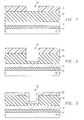
- Figure 1 illustrates, in cross-section, a partially formed integrated circuit structure at a surface of a wafer.
- an insulating layer 12 is formed to isolate devices or conductive layers.
- insulating layer 12 may be a field oxide region at a substrate surface 10 or may be an interlevel dielectric layer separating conducting regions or layers at different levels as known in the art.
- Conductive layer 14 lies over insulating layer 12, and is the structure to which connection is to be made in this invention.
- Insulating layer 16 is disposed over the conductive layer 14.
- the invention is equivalently applicable to contacts to a diffusion in the substrate, polysilicon electrodes, metal lines, and other structures in conventional integrated circuits. Furthermore, it should be noted that the present invention is also compatible with planarized processes, where contacts of different depths must be simultaneously made from the same planar surface (e.g. contacts to diffusion and polysilicon both made from the same planarized surface of silicon dioxide). Those skilled in the art will understand how to form a field oxide region or an interlevel dielectric layer 12.
- conductive layer 14 is shown as an interconnect line, which may a metal or doped polysilicon interconnect, formed by depositing a thin layer on the order of 2000 to 7000 angstroms.- As noted above, however, conductive layer 14 may also be a polysilicon electrode or a diffusion in the substrate or other structure in conventional integrated circuits.
- any suitable deposition process may be used consistent with the layer being formed, such as chemical vapor deposition, sputtering or vacuum evaporation. The unwanted regions of the conductive layer 14 are masked using standard photolithography techniques and etched, leaving the conductive lines or interconnects shown. If polysilicon is the preferred material, it may of course be doped in situ during the deposition process or may be doped after deposition.
- Insulating layer 16 may be any conventional insulator useful in modern integrated circuits, and preferably comprises a silicon dioxide, either as a single or as multiple layers.
- the thickness of layer 16 through which a subsequent contact or via opening will be made is on the order of 1.0 ⁇ m.
- photoresist layer 18 is formed over insulating layer 16 and is illustrated after it has been exposed and developed to define the smallest mask pattern achievable for the contact to be made.
- the resolution capability of the photoresist as well as the equipment used to correctly align and expose the photoresist will determine the particular size or contact dimension of opening 20.
- this will allow devices to be formed closer together thereby increasing packing density without reducing device integrity.
- these smaller openings may not be achievable with current photoresists and equipment.
- the technological needs continue to push the limits on photoresist equipment.
- insulating layer 16 is etched in opening 20 to form a contact opening partially through the insulating layer.
- the opening is preferably etched by an anisotropic etch such as reactive ion etching or other suitable means to take advantage of the ability to form substantially vertical sidewalls at the edges of opening 20 and to achieve better definition of small feature sizes on advance circuits.
- the width of the contact opening may be on the order of 0.5 ⁇ m or smaller.
- opening 20 is shown to continue partially through the insulating layer 16, preferably formed by a timed etch depending upon the thickness of the insulating layer.
- photoresist layer 18 is removed, for example, by a wet chemical strip or a plasma strip.
- a sidewall spacer film 22 is formed over insulating layer 16 and in opening 20.
- Sidewall spacer film 22 may be of any suitable material which may be selectively etched over the insulating layer 16, for example, polysilicon or nitride. This layer will be etched subsequently to leave sidewall spacers in contact opening 20, thus the thickness of this layer will depend upon the desired size of the resulting sidewall spacers, and is preferably on the order of 200 to 1000 angstroms.
- an anisotropic etchback of the sidewall spacer film is performed leaving sidewall spacers 24.
- the sidewall spacer film may be overetched such that the upper region 26 of spacers 24 lie below the upper surface 28 of insulating layer 16 by a distance which is approximately equal to the thickness "a" of the remaining insulating layer 16 in the bottom of the contact opening 20 above the conducting layer 14.
- This etch may be a timed etch similar to the timed etch used to partially etch the insulating layer 16 in opening 20.
- This sidewall formation has advantages over standard sidewall formation. The insulating layer 16, up to this point, remains in the bottom of opening 20.
- the underlying conducting layer 14 is designed to have a minimum width, then there is a greater possibility of trenching around layer 14 into the underlying dielectric layer 12, particularly if the original contact opening 20, before the sidewall spacers are formed, lies outside the width of layer 14. In the present invention, the possibility of trenching diminishes since the opening to layer 14 is not made until the contact dimension of opening 20 is reduced.
- the insulating layer 16 in the bottom of opening 20 is etched to expose the underlying conducting layer 14.
- an anisotropic etch selective to the material of the insulating layer over the sidewall spacers 24. This etch will achieve substantially vertical sidewalls at the bottom of contact opening 32. Insulating layer 16 at the bottom of contact opening 32 will etch at essentially the same rate as the upper surface 28 (shown in Figure 4). The thickness of the insulating layer removed at the upper surface 28 will be approximately the same as the amount removed in the bottom of the contact opening.
- the upper regions 26 of the sidewall spacers 24 lie below the upper surface 28 ( Figure 4) of insulating layer 16.
- the upper surface 26 of the sidewall spacers 24 may be substantially planar with the upper surface 30 ( Figure 5A) of the insulating layer 16.
- the contact dimension of the newly formed contact opening 32 with sidewall spacers 24 is now smaller than the original contact dimension of contact opening 20 prior to the formation of the sidewall spacers.
- the new contact dimension is smaller by twice the width "b" of each of the sidewall spacers 24.
- the contact dimension is now smaller than the lines which can be printed with photolithographic technology and materials.
- FIG. 5B an alternative of the first embodiment is shown whereby the sidewall spacers 24 may be removed prior to subsequent processing steps such as metallization.
- this may have the advantage of providing a contact or via with a smaller contact dimension at the bottom of the opening to meet device requirements and packing densities without adding substantially to step coverage problems.
- an overlying conductor may be formed with smaller dimensions due to the smaller effective opening at the top. The processes described above have the additional advantage of always staying one step ahead of the current photolithography technology.
- Figure 6 illustrates, in cross-section, a partially formed integrated circuit structure at a surface of a wafer.
- Insulating layer 12 is formed at a substrate surface 10.
- Conductive layer 14 lies over the insulating layer 12, and is the structure to which connection is to be made in the second alternative embodiment of the present invention.
- Insulating layer 16 is disposed over the conductive layer 14 and is illustrated after it has been etched to from opening 20.
- the invention is equivalently applicable to contacts to a diffusion in the substrate, polysilicon electrodes, metal lines, and other structures in conventional integrated circuits.
- Insulating layer 16 is etched to form a contact opening 20.
- the width of the contact opening may be on the order of 0.5 ⁇ m or smaller.
- Insulating layer 16 may be any conventional insulator useful in modern integrated circuits, and is generally silicon dioxide, either as a single or as multiple layers.
- the thickness of insulating layer 16 through which the contact opening is formed may be on the order of 1.0 ⁇ m.
- opening 20 is shown to continue through the insulating layer 16 exposing the conductive layer 14 in the bottom of the opening.
- the opening is preferably formed by an anisotropic etch to take advantage of the ability to form substantially vertical sidewalls.
- a thin layer of oxide 34 on the order of 100 to 300 angstroms may be deposited or grown to cover the exposed conducting layer 14 in the bottom of opening 20 to protect the conducting layer during subsequent processing steps.
- a thin layer of polysilicon 36 is deposited over insulating layer 16 and in opening 20.
- polysilicon layer 36 is oxidized to convert the polysilicon to an oxide 36' having a thickness on the order of approximately two (2) times the original thickness of polysilicon layer 36.
- Moisture and oxygen added to the system after the polysilicon is deposited causes the growth of silicon dioxide within the polysilicon structure converting the polysilicon into oxide and expanding the polysilicon accordingly, thereby decreasing the contact dimension within opening 20 by approximately four (4) times the thickness of standard deposited polysilicon.
- the thickness of the thin polysilicon layer 36 before oxidation is approximately one-half of the thickness of the oxidized polysilicon 36' and is more particularly determined based upon the desired final contact dimension and may be on the order of 100 to 500 angstroms.
- the resulting oxidized polysilicon thickness accordingly will be on the order of 200 to 1000 angstroms.
- the oxidation process may vary the resulting contact dimension and may reduce the contact dimension of the opening by as much as a 2:1 ratio depending on the polysilicon film thickness and the original contact size.
- the oxidized polysilicon layer 36' is anisotropically etched to form oxidized polysilicon sidewalls 38. If the thin oxide layer 34 was first formed, it will protect the surface of the underlying conductive layer 14 in opening 20 during the etch of the polysilicon layer 36' and then may be subsequently etched to expose layer 14. Polysilicon layer 36 may be doped with an appropriate dopant during or after deposition to provide a more uniform etch and oxidation rate particularly at lower oxidation temperatures.
- the oxidized polysilicon is preferred over the formation of an oxide of the same final thickness since growth or deposition of a thick oxide tends to cause cusping at the corners.
- the oxidized polysilicon limits the cusping problems associated with deposited thicker oxides.
- the width of the newly formed contact opening 40 now has a contact dimension smaller than the original contact dimension.
- the new contact dimension is smaller by twice the width "b" of each of the sidewall spacers 38.
- the contact dimension is now smaller than what is manufacturable with current state-of-the-art photolithography equipment.
- Figure 9 illustrates, in cross-section, a partially formed integrated circuit structure at a surface of a wafer.
- Insulating layer 12 is formed at a substrate surface 10.
- Conductive layer 14 lies over the insulating layer 12, and is the structure to which connection is to be made in the third alternative embodiment of the present invention.
- an etch stop layer 42 is shown disposed over the conductive layer 14.
- Etch stop layer 42 is deposited to a thickness on the order of 250 to 1000 angstroms and will protect the conductive layer during particular subsequent processing steps.
- the material for this layer should be chosen such that it may be selectively etched over the conductive layer 14.
- a nitride or other suitable material may be selectively etched without substantially etching the underlying conductive layer 14.
- Insulating layer 16 is illustrated after it has been etched to form opening 20 and is disposed over the conductive layer 14.
- this embodiment of the invention is also equivalently applicable to contacts to a diffusion in the substrate, polysilicon electrodes, metal lines, and other structures in conventional integrated circuits.
- opening 20 is shown to continue through the insulating layer 16, preferably by a timed etch or end-point detection etch.
- the opening is preferably formed by an anisotropic etch to take advantage of the ability to form substantially vertical sidewalls along the sides of opening 20.
- a sidewall spacer film 44 is formed over insulating layer 16 and in opening 20.
- Sidewall spacer film 44 may be of any suitable material which may be selectively etched over the insulating layer 16 and having substantially the same etch rate as the etch stop layer 42. This layer will be etched to leave sidewall spacers in contact opening 20, thus the thickness of this layer will depend upon the desired contact dimension using the sidewall spacers to achieve this internal final contact or via dimension, and is preferably on the order of 200 to 1000 angstroms.
- the sidewall spacer film 44 is anisotropically etched to form sidewall spacers 46. This etch step will continue through the etch stop layer and expose the conductive layer 14 in opening 48. Since the sidewall spacer film is overetched by the thickness of the etch stop layer, the sidewall spacers will be etched by a similar amount and may be below the upper region 50 of insulating layer 16. The smallest contact dimension of the original opening 20 provided for by the current photolithography equipment has now been reduced to a smaller contact dimension determined by twice the width of each of the sidewall spacers 46 in the new opening 48.
- Figure 11 illustrates a contact 52 made to the underlying conductive region 14 through opening. Those skilled in the art will appreciate that similar contacts may be formed in the alternate embodiments described above.
- Figure 12 illustrates, in cross-section, a partially formed integrated circuit structure at a surface of a wafer.
- Insulating layer 12 is formed at a substrate surface 10.
- Conductive layer 14 lies over the insulating layer 12, and is the structure to which connection is to be made in the fourth alternative embodiment of the present invention.
- Insulating layer 16 is shown disposed over the conductive layer 14.
- this embodiment of the invention is also equivalently applicable to contacts to a diffusion in the substrate, polysilicon electrodes, metal lines, and other structures in conventional integrated circuits.
- a thin etch stop layer 54 is formed over insulating layer 16.
- This etch stop layer is preferably nitride or polysilicon or any other suitable material which will have a different etch rate than insulating layer 16 for a given etchant.
- Layer 54 is preferably deposited by chemical vapor deposition to a thickness on the order of 100 to 1000 angstroms.
- a sacrificial insulating layer 56 is formed over the etch stop layer 54.
- Layer 56 may be any suitable material such as an oxide which also has an etch rate different than the etch stop layer for a given etchant.
- Layer 54 is preferably a deposited oxide having a thickness on the order of 200 to 1000 angstroms. While layer 54 is shown here as planar, it is a conformal layer and will follow the contour of the underlying topography. If the oxide is deposited thick enough, it will tend to become more planar, particularly as it deposits over closely spaced devices and regions.
- a photoresist layer 58 is formed over the sacrificial oxide layer 56 and is illustrated after it has been exposed and developed to define a small mask pattern for making the desired contact having a contact dimension 62. As described above, the resolution capability of the photoresist as well as the equipment used to correctly align and expose the photoresist will determine the particular size or contact dimension 62 of opening 60.
- the sacrificial oxide layer 56 is etched in opening 60 to expose a portion of the underlying etch stop layer 54.
- This etch step is preferably a endpoint detection etch which will stop when the etch stop layer is reached.
- the photoresist layer 58 is removed by methods known in the art, for example, by a wet chemical strip or a plasma strip.
- a sidewall spacer film 64 is formed over the sacrificial oxide layer 56 and in the opening 60 along the sidewalls of insulating layer 56 and the exposed etch stop layer 54 to a thickness on the order of 200 to 1000 angstroms.
- the sidewall spacer film 64 preferably has a similar etch ratio as the underlying etch stop layer 56 for a given etchant and may be a nitride or polysilicon or other suitable material. It is important that film 64 and etch stop layer 54 have an etch rate different than conductive layer 14 for reasons described below.
- the sidewall spacer film 64 and etch stop layer 54 are anisotropically etched to expose the underlying insulating layer 16 in opening 60.
- a sidewall spacer 66 is formed along the sidewalls of insulating layer 16. This etch step is preferably an endpoint detection etch which will stop when the insulating layer 16 is reached. Both the spacer film and etch stop layers must be etched in the bottom of the opening and because of the total thickness, an overetch of the spacer film is likely to result such that the upper surface of the spacers 66 is below the upper surface of insulating layer 56.
- the contact dimension 68 of opening 60 is now smaller than the original contact dimension 62 of opening 60 by the width "c" of each of the sidewall spacers 66. This contact dimension is smaller than the dimension which can be printed with modern photolithographic techniques and equipment.
- an opening 70 is anisotropically etched in insulating layer 16 to expose the underlying conductive layer 14. This etch step will also remove the sacrificial oxide layer 56 if the etch rates for these two layers are similar for a given etchant. Any sacrificial oxide remaining is removed using the etch stop layer to prevent overetching the insulating layer 16.
- the sidewall spacers 64 and etch stop layer 54 are preferably removed to provide a more planar surface before subsequent processing steps take place. In addition, removing the spacers and etch stop layer will lower the aspect ratio of opening 70 through insulating layer 16. In order to avoid etching any substantial portion of conductive layer 14 in opening 70, it is preferable that the etch rates for spacers 66 and etch stop layer 54 are different than conductive layer 14 for a given etchant.
- a contact 72 is illustrated making contact to the underlying conductive layer 14 and is formed by methods known in the art. As described above, the contact dimension of opening 70 is smaller than the contact dimension which can be printed with state-of-of-the-art lithographic processes and equipment.
- the packing density and geometries and dimensions of features underlying the contact or via opening may be similarly scaled. This process of reducing the minimum feature sizes can be continually scaled to achieve the desired geometries and dimensions not otherwise achievable with modern photolithography equipment and materials.
Landscapes
- Internal Circuitry In Semiconductor Integrated Circuit Devices (AREA)
- Drying Of Semiconductors (AREA)
Applications Claiming Priority (2)
| Application Number | Priority Date | Filing Date | Title |
|---|---|---|---|
| US574659 | 1995-12-19 | ||
| US08/574,659 US5847460A (en) | 1995-12-19 | 1995-12-19 | Submicron contacts and vias in an integrated circuit |
Publications (2)
| Publication Number | Publication Date |
|---|---|
| EP0780894A2 true EP0780894A2 (de) | 1997-06-25 |
| EP0780894A3 EP0780894A3 (de) | 1997-08-27 |
Family
ID=24297060
Family Applications (1)
| Application Number | Title | Priority Date | Filing Date |
|---|---|---|---|
| EP96309299A Withdrawn EP0780894A3 (de) | 1995-12-19 | 1996-12-19 | Verfahren zur Herstellung von Submikron-Durchgangslöchern und -Kontakten in einer integrierten Schaltung |
Country Status (3)
| Country | Link |
|---|---|
| US (2) | US5847460A (de) |
| EP (1) | EP0780894A3 (de) |
| JP (1) | JPH09181180A (de) |
Families Citing this family (46)
| Publication number | Priority date | Publication date | Assignee | Title |
|---|---|---|---|---|
| JPH0997833A (ja) * | 1995-07-22 | 1997-04-08 | Ricoh Co Ltd | 半導体装置とその製造方法 |
| US6111319A (en) * | 1995-12-19 | 2000-08-29 | Stmicroelectronics, Inc. | Method of forming submicron contacts and vias in an integrated circuit |
| KR0176199B1 (ko) * | 1996-03-19 | 1999-04-15 | 김광호 | 반도체 소자의 접촉창 형성방법 |
| US6337266B1 (en) | 1996-07-22 | 2002-01-08 | Micron Technology, Inc. | Small electrode for chalcogenide memories |
| US5789277A (en) * | 1996-07-22 | 1998-08-04 | Micron Technology, Inc. | Method of making chalogenide memory device |
| EP0881669B1 (de) * | 1997-05-30 | 2005-12-14 | STMicroelectronics S.r.l. | Verfahren zur Herstellung eines Germanium-implantierten bipolaren Heteroübergangtransistors |
| US6028363A (en) * | 1997-06-04 | 2000-02-22 | Taiwan Semiconductor Manufacturing Company | Vertical via/contact |
| EP0921562A3 (de) * | 1997-10-28 | 2002-06-05 | Texas Instruments Incorporated | Verbesserungen an oder in Beziehung zu Leiterrahmen |
| KR100396110B1 (ko) * | 1998-03-10 | 2003-08-27 | 인터내셔널 비지네스 머신즈 코포레이션 | 이중 직경 컨택트 플러그 및 그 제조 방법 |
| US6496352B2 (en) * | 1998-06-30 | 2002-12-17 | Texas Instruments Incorporated | Post-in-crown capacitor and method of manufacture |
| DE19843624C1 (de) * | 1998-09-23 | 2000-06-15 | Siemens Ag | Integrierte Schaltungsanordnung und Verfahren zu deren Herstellung |
| US6228699B1 (en) * | 1998-12-14 | 2001-05-08 | Taiwan Semiconductor Manufacturing Company | Cross leakage of capacitors in DRAM or embedded DRAM |
| TW426961B (en) * | 1999-08-03 | 2001-03-21 | United Microelectronics Corp | Fabrication method of node contact hole opening |
| US6136695A (en) * | 1999-08-04 | 2000-10-24 | Taiwan Semiconductor Manufacturing Company | Method for fabricating a self-aligned contact |
| US6124197A (en) | 1999-10-01 | 2000-09-26 | Advanced Micro Devices, Inc. | Adjusting the size of conductive lines based upon contact size |
| JP2001110782A (ja) * | 1999-10-12 | 2001-04-20 | Oki Electric Ind Co Ltd | 半導体装置の製造方法 |
| US6551923B1 (en) | 1999-11-01 | 2003-04-22 | Advanced Micro Devices, Inc. | Dual width contact for charge gain reduction |
| US6441418B1 (en) * | 1999-11-01 | 2002-08-27 | Advanced Micro Devices, Inc. | Spacer narrowed, dual width contact for charge gain reduction |
| JP3547364B2 (ja) * | 2000-04-21 | 2004-07-28 | シャープ株式会社 | 半導体装置の製造方法 |
| US6413792B1 (en) | 2000-04-24 | 2002-07-02 | Eagle Research Development, Llc | Ultra-fast nucleic acid sequencing device and a method for making and using the same |
| US8232582B2 (en) * | 2000-04-24 | 2012-07-31 | Life Technologies Corporation | Ultra-fast nucleic acid sequencing device and a method for making and using the same |
| US7001792B2 (en) * | 2000-04-24 | 2006-02-21 | Eagle Research & Development, Llc | Ultra-fast nucleic acid sequencing device and a method for making and using the same |
| DE10030442B4 (de) * | 2000-06-22 | 2006-01-12 | Infineon Technologies Ag | Verbindungselement in einem integrierten Schaltkreis |
| US6358800B1 (en) * | 2000-09-18 | 2002-03-19 | Vanguard International Semiconductor Corporation | Method of forming a MOSFET with a recessed-gate having a channel length beyond photolithography limit |
| DE10052419B4 (de) * | 2000-10-23 | 2006-10-19 | Infineon Technologies Ag | Verfahren zur Herstellung mikromechanischer Bauelemente |
| US6869879B1 (en) * | 2000-11-03 | 2005-03-22 | Advancedmicro Devices, Inc. | Method for forming conductive interconnects |
| US6972448B2 (en) * | 2000-12-31 | 2005-12-06 | Texas Instruments Incorporated | Sub-lithographics opening for back contact or back gate |
| WO2002054450A2 (en) * | 2001-01-04 | 2002-07-11 | Eagle Research & Development, Llc | Method of patterning a mask on the surface of a substrate and product manufactured thereby |
| US6660456B2 (en) | 2001-06-27 | 2003-12-09 | International Business Machines Corporation | Technique for the size reduction of vias and other images in semiconductor chips |
| KR100428791B1 (ko) * | 2002-04-17 | 2004-04-28 | 삼성전자주식회사 | 저유전율 절연막을 이용한 듀얼 다마신 배선 형성방법 |
| KR20040000752A (ko) * | 2002-06-25 | 2004-01-07 | 동부전자 주식회사 | 반도체 소자의 제조 방법 |
| US6924221B2 (en) * | 2002-12-03 | 2005-08-02 | Taiwan Semiconductor Manufacturing Co., Ltd. | Integrated process flow to improve copper filling in a damascene structure |
| CN1299349C (zh) * | 2004-04-28 | 2007-02-07 | 联华电子股份有限公司 | 双镶嵌工艺中两阶段去除介层洞光刻胶的方法 |
| US20060019497A1 (en) * | 2004-07-22 | 2006-01-26 | Zhizhang Chen | Reduced feature-size memory devices and methods for fabricating the same |
| KR100611776B1 (ko) * | 2004-10-06 | 2006-08-10 | 주식회사 하이닉스반도체 | 반도체 소자 제조 방법 |
| DE102005020132B4 (de) * | 2005-04-29 | 2011-01-27 | Advanced Micro Devices, Inc., Sunnyvale | Technik zur Herstellung selbstjustierter Durchführungen in einer Metallisierungsschicht |
| US7488680B2 (en) | 2005-08-30 | 2009-02-10 | International Business Machines Corporation | Conductive through via process for electronic device carriers |
| US20080113483A1 (en) * | 2006-11-15 | 2008-05-15 | Micron Technology, Inc. | Methods of etching a pattern layer to form staggered heights therein and intermediate semiconductor device structures |
| JP4389962B2 (ja) * | 2007-04-26 | 2009-12-24 | ソニー株式会社 | 半導体装置、電子機器、および半導体装置の製造方法 |
| KR101033222B1 (ko) * | 2007-06-29 | 2011-05-06 | 주식회사 하이닉스반도체 | 전하트랩층을 갖는 불휘발성 메모리소자의 제조방법 |
| JP2009099854A (ja) * | 2007-10-18 | 2009-05-07 | Elpida Memory Inc | 縦型相変化メモリ装置の製造方法 |
| US8435874B2 (en) * | 2008-01-23 | 2013-05-07 | Freescale Semiconductor, Inc. | Method of forming openings in a semiconductor device and a semiconductor device fabricated by the method |
| DE102009023251B4 (de) * | 2009-05-29 | 2011-02-24 | Globalfoundries Dresden Module One Limited Liability Company & Co. Kg | Verfahren zur Herstellung eines Kontaktelements mit großem Aspektverhältnis und mit einer günstigeren Form in einem Halbleiterbauelement zur Verbesserung der Abscheidung einer Beschichtung |
| US9018090B2 (en) * | 2011-10-10 | 2015-04-28 | International Business Machines Corporation | Borderless self-aligned metal contact patterning using printable dielectric materials |
| FR3064399B1 (fr) * | 2017-03-22 | 2019-05-03 | Stmicroelectronics (Crolles 2) Sas | Transistor quantique vertical |
| CN114664790B (zh) * | 2022-05-24 | 2022-08-09 | 合肥晶合集成电路股份有限公司 | 一种集成电路结构及其形成方法 |
Family Cites Families (39)
| Publication number | Priority date | Publication date | Assignee | Title |
|---|---|---|---|---|
| JPS4835778A (de) * | 1971-09-09 | 1973-05-26 | ||
| JPS5750429A (en) * | 1980-09-12 | 1982-03-24 | Nec Corp | Manufacture of semiconductor device |
| US4472240A (en) * | 1981-08-21 | 1984-09-18 | Tokyo Shibaura Denki Kabushiki Kaisha | Method for manufacturing semiconductor device |
| US4720908A (en) * | 1984-07-11 | 1988-01-26 | Texas Instruments Incorporated | Process for making contacts and interconnects for holes having vertical sidewalls |
| US4656732A (en) * | 1984-09-26 | 1987-04-14 | Texas Instruments Incorporated | Integrated circuit fabrication process |
| US4677739A (en) * | 1984-11-29 | 1987-07-07 | Texas Instruments Incorporated | High density CMOS integrated circuit manufacturing process |
| JPS62133713A (ja) * | 1985-12-06 | 1987-06-16 | Hitachi Ltd | 電極形成方法およびその電極 |
| US5067002A (en) * | 1987-01-30 | 1991-11-19 | Motorola, Inc. | Integrated circuit structures having polycrystalline electrode contacts |
| US4960732A (en) * | 1987-02-19 | 1990-10-02 | Advanced Micro Devices, Inc. | Contact plug and interconnect employing a barrier lining and a backfilled conductor material |
| GB2206729B (en) * | 1987-07-01 | 1990-10-24 | British Aerospace | A method of forming electrical contacts in a multi-level interconnect system |
| US5094079A (en) * | 1987-10-22 | 1992-03-10 | Automotive Products Plc | Master cylinder assembly |
| US4962414A (en) * | 1988-02-11 | 1990-10-09 | Sgs-Thomson Microelectronics, Inc. | Method for forming a contact VIA |
| US4872050A (en) * | 1988-03-15 | 1989-10-03 | Mitsubishi Denki Kabushiki Kaisha | Interconnection structure in semiconductor device and manufacturing method of the same |
| JP2675572B2 (ja) * | 1988-03-31 | 1997-11-12 | 株式会社東芝 | 半導体集積回路の製造方法 |
| US4994410A (en) * | 1988-04-04 | 1991-02-19 | Motorola, Inc. | Method for device metallization by forming a contact plug and interconnect using a silicide/nitride process |
| US4837183A (en) * | 1988-05-02 | 1989-06-06 | Motorola Inc. | Semiconductor device metallization process |
| JPH01289142A (ja) * | 1988-05-16 | 1989-11-21 | Nippon Telegr & Teleph Corp <Ntt> | 垂直配線構造 |
| FR2634317A1 (fr) * | 1988-07-12 | 1990-01-19 | Philips Nv | Procede pour fabriquer un dispositif semiconducteur ayant au moins un niveau de prise de contact a travers des ouvertures de contact de petites dimensions |
| IT1225631B (it) * | 1988-11-16 | 1990-11-22 | Sgs Thomson Microelectronics | Rastremazione di fori attraverso strati dielettrici per formare contatti in dispositivi integrati. |
| JPH02231712A (ja) * | 1989-03-03 | 1990-09-13 | Mitsubishi Electric Corp | 半導体装置の製造方法 |
| EP0388563B1 (de) * | 1989-03-24 | 1994-12-14 | STMicroelectronics, Inc. | Verfahren zum Herstellen eines Kontaktes/VIA |
| US5117273A (en) * | 1990-11-16 | 1992-05-26 | Sgs-Thomson Microelectronics, Inc. | Contact for integrated circuits |
| US5270254A (en) * | 1991-03-27 | 1993-12-14 | Sgs-Thomson Microelectronics, Inc. | Integrated circuit metallization with zero contact enclosure requirements and method of making the same |
| US5120679A (en) * | 1991-06-04 | 1992-06-09 | Vlsi Technology, Inc. | Anti-fuse structures and methods for making same |
| JP3166221B2 (ja) * | 1991-07-23 | 2001-05-14 | 日本電気株式会社 | 半導体装置及びその製造方法 |
| US5294295A (en) * | 1991-10-31 | 1994-03-15 | Vlsi Technology, Inc. | Method for moisture sealing integrated circuits using silicon nitride spacer protection of oxide passivation edges |
| JPH0629406A (ja) * | 1991-11-18 | 1994-02-04 | Sony Corp | コンタクト構造及びそのコンタクト形成方法 |
| US5384483A (en) * | 1992-02-28 | 1995-01-24 | Sgs-Thomson Microelectronics, Inc. | Planarizing glass layer spaced from via holes |
| US5321211A (en) * | 1992-04-30 | 1994-06-14 | Sgs-Thomson Microelectronics, Inc. | Integrated circuit via structure |
| US5262352A (en) * | 1992-08-31 | 1993-11-16 | Motorola, Inc. | Method for forming an interconnection structure for conductive layers |
| KR100260577B1 (ko) * | 1992-09-09 | 2000-08-01 | 김영환 | 자기정렬형 콘택 형성방법 |
| KR0136569B1 (ko) * | 1992-10-24 | 1998-04-29 | 김주용 | 고집적 반도체 소자의 콘택홀 형성 방법 |
| JP2787646B2 (ja) * | 1992-11-27 | 1998-08-20 | 三菱電機株式会社 | 半導体装置の製造方法 |
| US5514900A (en) * | 1994-03-31 | 1996-05-07 | Crosspoint Solutions, Inc. | Mutlilayered antifuse with intermediate metal layer |
| US5439838A (en) * | 1994-09-14 | 1995-08-08 | United Microelectronics Corporation | Method of thinning for EEPROM tunneling oxide device |
| US5512785A (en) * | 1994-11-30 | 1996-04-30 | Motorola, Inc. | Semiconducter device having an emitter terminal separated from a base terminal by a composite nitride/oxide layer |
| US5614765A (en) * | 1995-06-07 | 1997-03-25 | Advanced Micro Devices, Inc. | Self aligned via dual damascene |
| KR0186085B1 (ko) * | 1995-09-02 | 1999-04-15 | 문정환 | 배선 형성방법 |
| US5658830A (en) * | 1996-07-12 | 1997-08-19 | Vanguard International Semiconductor Corporation | Method for fabricating interconnecting lines and contacts using conformal deposition |
-
1995
- 1995-12-19 US US08/574,659 patent/US5847460A/en not_active Expired - Lifetime
-
1996
- 1996-12-17 JP JP8336704A patent/JPH09181180A/ja active Pending
- 1996-12-19 EP EP96309299A patent/EP0780894A3/de not_active Withdrawn
-
1997
- 1997-11-25 US US08/978,382 patent/US6033980A/en not_active Expired - Lifetime
Non-Patent Citations (1)
| Title |
|---|
| None |
Also Published As
| Publication number | Publication date |
|---|---|
| JPH09181180A (ja) | 1997-07-11 |
| US5847460A (en) | 1998-12-08 |
| EP0780894A3 (de) | 1997-08-27 |
| US6033980A (en) | 2000-03-07 |
Similar Documents
| Publication | Publication Date | Title |
|---|---|---|
| US6033980A (en) | Method of forming submicron contacts and vias in an integrated circuit | |
| US6180517B1 (en) | Method of forming submicron contacts and vias in an integrated circuit | |
| US5726100A (en) | Method of forming contact vias and interconnect channels in a dielectric layer stack with a single mask | |
| US6165889A (en) | Process for forming trenches and contacts during the formation of a semiconductor memory device | |
| US4767724A (en) | Unframed via interconnection with dielectric etch stop | |
| US5087591A (en) | Contact etch process | |
| EP0905768A1 (de) | Doppel-Damascenen Verfahren für Metallschichten und organische Schichten zwischen zwei Metallisierungen | |
| US5977599A (en) | Formation of a metal via using a raised metal plug structure | |
| US5593921A (en) | Method of forming vias | |
| KR100277377B1 (ko) | 콘택트홀/스루홀의형성방법 | |
| US4933297A (en) | Method for etching windows having different depths | |
| US7049206B2 (en) | Device isolation for semiconductor devices | |
| EP0558260A1 (de) | Herstellungsverfahren von Kontaktöffnungen in integrierten Schaltungen | |
| US6350682B1 (en) | Method of fabricating dual damascene structure using a hard mask | |
| JPH08335634A (ja) | 半導体装置の製造方法 | |
| US6566236B1 (en) | Gate structures with increased etch margin for self-aligned contact and the method of forming the same | |
| US6222255B1 (en) | Method of creating an interconnect in a substrate and semiconductor device employing the same | |
| EP1435656A2 (de) | Herstellung einer Doppel-Damaszener-Verbindungsstruktur | |
| KR100299379B1 (ko) | 반도체소자의금속배선형성방법 | |
| KR0165453B1 (ko) | Y자형 트랜치를 이용한 반도체 소자의 분리 방법 | |
| US5847457A (en) | Structure and method of forming vias | |
| KR100328557B1 (ko) | 반도체 소자의 금속배선 형성방법 | |
| KR100204910B1 (ko) | 반도체장치의 배선들의 접촉 방법 | |
| KR100772077B1 (ko) | 반도체 소자의 콘택홀 형성방법 | |
| KR100209279B1 (ko) | 반도체 소자의 콘택홀 형성방법 |
Legal Events
| Date | Code | Title | Description |
|---|---|---|---|
| PUAI | Public reference made under article 153(3) epc to a published international application that has entered the european phase |
Free format text: ORIGINAL CODE: 0009012 |
|
| AK | Designated contracting states |
Kind code of ref document: A2 Designated state(s): DE FR GB IT |
|
| PUAL | Search report despatched |
Free format text: ORIGINAL CODE: 0009013 |
|
| AK | Designated contracting states |
Kind code of ref document: A3 Designated state(s): DE FR GB IT |
|
| 17P | Request for examination filed |
Effective date: 19980202 |
|
| RAP3 | Party data changed (applicant data changed or rights of an application transferred) |
Owner name: STMICROELECTRONICS, INC. |
|
| STAA | Information on the status of an ep patent application or granted ep patent |
Free format text: STATUS: THE APPLICATION HAS BEEN WITHDRAWN |
|
| 18W | Application withdrawn |
Withdrawal date: 19991214 |