EP0778673A1 - Circuit intégré avec circuit d'attaque de sortie programmable - Google Patents
Circuit intégré avec circuit d'attaque de sortie programmable Download PDFInfo
- Publication number
- EP0778673A1 EP0778673A1 EP96118287A EP96118287A EP0778673A1 EP 0778673 A1 EP0778673 A1 EP 0778673A1 EP 96118287 A EP96118287 A EP 96118287A EP 96118287 A EP96118287 A EP 96118287A EP 0778673 A1 EP0778673 A1 EP 0778673A1
- Authority
- EP
- European Patent Office
- Prior art keywords
- driver
- integrated circuit
- programming unit
- drivers
- pad
- Prior art date
- Legal status (The legal status is an assumption and is not a legal conclusion. Google has not performed a legal analysis and makes no representation as to the accuracy of the status listed.)
- Granted
Links
- 230000003213 activating effect Effects 0.000 claims 1
- 230000006870 function Effects 0.000 claims 1
- 238000010586 diagram Methods 0.000 description 6
- 238000005259 measurement Methods 0.000 description 2
- 230000003068 static effect Effects 0.000 description 2
- 238000000034 method Methods 0.000 description 1
- 230000000630 rising effect Effects 0.000 description 1
- 238000011144 upstream manufacturing Methods 0.000 description 1
Images

Classifications
-
- H—ELECTRICITY
- H03—ELECTRONIC CIRCUITRY
- H03K—PULSE TECHNIQUE
- H03K19/00—Logic circuits, i.e. having at least two inputs acting on one output; Inverting circuits
- H03K19/0175—Coupling arrangements; Interface arrangements
- H03K19/017581—Coupling arrangements; Interface arrangements programmable
Definitions
- the pad drivers (connection contact drivers) of integrated circuits have to be adapted to the external load, for example to achieve soft "voltage and current profiles on the signal lines.
- the EMC-optimal driver is not available for all load cases. Rather, the signal form depends both on the dimensioning, in particular on the driver strength I in amperes and the slope dU / dt in V / sec, of the driver and on the type of load, for example a capacitive load, an open line or a line network. Since an integrated circuit is generally not only used for a specific application with a clearly defined load environment, EMC-optimal dimensioning of the pad drivers is only possible for specific applications.
- a digital driver circuit for integrated circuit which can be adapted to a load capacitance by connecting a corresponding number of output branches.
- the driver circuit is comparatively complex since, in addition to the output branches, control means for actuating the output branches, an input device for entering a measurement number, a setting means for determining a manipulated variable assigned to a specific output branch on the basis of the measurement number and a switching means for releasing the specific output branches are provided.
- a driver circuit is known from German published patent application DE 42 00 680 A1, in which a plurality of drivers are used the slope of the positive and negative signal edges is set separately by partial drivers.
- the object on which the invention is based is to provide an integrated circuit with a pad driver, the driver properties of which, such as driver strength I in amperes and the slope steepness dU / dt in V / sec, can be flexibly adapted to a respective external load , for which the smallest possible additional chip area should be aimed for.
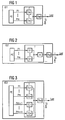
- FIG. 1 shows a first embodiment IS1 of an integrated circuit according to the invention, which has a programming unit PE, a driver T and a connection contact pad.
- a voltage U is present at the connection contact pad and a driver current I flows to the load, which is also designated.
- the driver T is equipped with several partial drivers T1..Tm connected in parallel, the outputs of which are all connected to a common connection contact pad and which can be activated with the aid of programming signals P1 ... Pm from a programming unit PE as required.
- a deactivated partial driver has a high resistance at its output.
- the total driver strength I of the driver T is the sum of the driver strengths I1 + I2 ... of all activated partial drivers T1, T2 ...
- the driver strengths of the individual sub-drivers do not have to be equally distributed.
- FIG. 2 shows a second embodiment IS2 of an integrated circuit according to the invention, which essentially differs from the embodiment IS1 shown in FIG. 1 only in that the driver T with only one output stage A and a plurality of control units S1 ... connected upstream of the output stage. Sm is equipped, the output of the output stage A being connected to the connection contact pad and the respective inputs of the respective control units being able to be activated as required via programming signals P1 ... Pm from a programming unit PE.
- the dimensioning of A essentially determines the static driver strength I, the dimensioning of the control units, however, the edge steepness dU / dt.
- the slope of the driver T can be set accordingly by connecting several controls S1..Sm in parallel.
- FIG. 3 shows a third embodiment IS3 of an integrated circuit according to the invention, which essentially differs from the embodiment IS1 in FIG. 1 in that the driver T via partial drivers TU1 ... TUm for charging the load and partial driver TD1 ... TDn for unloading the load, whereby the positive and negative edge of the output signal can be optimized separately with regard to EMC.
- the partial drivers TU1 ... TUm are activated or deactivated by the programming signals P1 ... Pm and the partial drivers TD1 ... TDm by further programming signals Pm + 1 ... Pm + n.
- the programming of the programming unit PE can already be done by the manufacturer of the integrated circuit, e.g. as mask-programmable ROM, or, as indicated in FIGS. 4 and 5, carried out by the board developer.
- FIG. 4 shows a fourth embodiment IS4 of an integrated circuit according to the invention, which essentially differs from embodiment 1 in that a programming bit PB for programming the programming unit PE can be fed to the programming unit PE via the connection contact pad and in that the programming unit PE has a Control signal PR can be controlled from a control register flag or an additional connection pin.
- PR 1
- FIG. 5 shows a fifth embodiment IS5 of an integrated circuit according to the invention, which essentially differs from the embodiment IS4 in that at least one respective additional driver T is provided, which is also controlled with the programming signals P1..Pm, which is controlled with at least a further connection contact pad is connected and which, however, has no connection between the connection contact pad and the programming unit PE.
- the dynamic output signals e.g. B. addresses or data
- only a subset of all drivers needs a programming unit. If the load conditions of an address or data bus are similar for all lines, all associated pad drivers can be programmed in the same way with regard to EMC.
- the programming bit PB can optionally be supplied from any of the connection contacts pad.
- FIG. 6 shows a sixth embodiment IS6 of an integrated circuit according to the invention, which represents a combination of the drivers shown in the previous figures, with pad driver T without an associated programming unit PE, different pad drivers T with a separate programming unit and groups of pad modules. Drivers with a common programming unit are available. This makes different programming signals PR1 ..PR3 necessary.
- the programming unit PE is integrated on an integrated circuit according to the invention, for example in the pad frame, where there are often gaps.
- the programming unit PE stores the logical state of the programming signals, since these must be applied statically to the partial drivers so that their scaling does not change during operation.
- the programming signals can be stored in a volatile memory, for example in a RAM or a flip-flop, or else in a non-volatile memory, such as in a ROM, OTP, EEPROM or fuse.
Landscapes
- Engineering & Computer Science (AREA)
- Computer Hardware Design (AREA)
- Physics & Mathematics (AREA)
- Computing Systems (AREA)
- General Engineering & Computer Science (AREA)
- Mathematical Physics (AREA)
- Semiconductor Integrated Circuits (AREA)
- Tests Of Electronic Circuits (AREA)
- Read Only Memory (AREA)
- Design And Manufacture Of Integrated Circuits (AREA)
Applications Claiming Priority (2)
| Application Number | Priority Date | Filing Date | Title |
|---|---|---|---|
| DE19545904A DE19545904C2 (de) | 1995-12-08 | 1995-12-08 | Integrierte Schaltung mit programmierbarem Pad-Treiber |
| DE19545904 | 1995-12-08 |
Publications (2)
| Publication Number | Publication Date |
|---|---|
| EP0778673A1 true EP0778673A1 (fr) | 1997-06-11 |
| EP0778673B1 EP0778673B1 (fr) | 2000-05-24 |
Family
ID=7779606
Family Applications (1)
| Application Number | Title | Priority Date | Filing Date |
|---|---|---|---|
| EP96118287A Expired - Lifetime EP0778673B1 (fr) | 1995-12-08 | 1996-11-14 | Circuit intégré avec circuit d'attaque de sortie programmable |
Country Status (3)
| Country | Link |
|---|---|
| US (1) | US5834955A (fr) |
| EP (1) | EP0778673B1 (fr) |
| DE (2) | DE19545904C2 (fr) |
Cited By (2)
| Publication number | Priority date | Publication date | Assignee | Title |
|---|---|---|---|---|
| EP0913943A2 (fr) * | 1997-10-29 | 1999-05-06 | Hewlett-Packard Company | Circuit intégré dont les caractéristiques des bornes de sortie sont spécifiques à une application et méthode de fonctionnement |
| DE19841757C1 (de) * | 1998-09-11 | 2000-03-02 | Siemens Ag | Schaltungsanordnung zur Anpassung des Ausgangssignals eines Ausgangstreibers an die gegebenen Verhältnisse |
Families Citing this family (11)
| Publication number | Priority date | Publication date | Assignee | Title |
|---|---|---|---|---|
| JP3369807B2 (ja) | 1995-08-30 | 2003-01-20 | 株式会社東芝 | 半導体装置 |
| DE19901460C1 (de) | 1999-01-15 | 2000-08-31 | Siemens Ag | Integrierte Halbleiterschaltung und Verfahren zur Überprüfung des Übertragungsverhaltens von Pad-Zellen |
| US6271699B1 (en) | 1999-04-02 | 2001-08-07 | Motorola, Inc. | Driver circuit and method for controlling transition time of a signal |
| US6483879B1 (en) | 1999-08-27 | 2002-11-19 | Lsi Logic Corporation | Compensating for initial signal interference exhibited by differential transmission lines |
| DE10036863C2 (de) * | 2000-07-28 | 2002-09-19 | Texas Instruments Deutschland | Treiberschaltung zur Abgabe eines einstellbaren Ausgangssignalstroms |
| US7132868B2 (en) | 2001-06-27 | 2006-11-07 | Mitsubishi Denki Kabushiki Kaisha | Semiconductor device |
| DE10148338B4 (de) | 2001-09-29 | 2005-11-10 | Infineon Technologies Ag | Skalierbare Treibervorrichtung sowie zugehörige integrierte Schaltung |
| KR100567077B1 (ko) | 2005-01-31 | 2006-04-04 | 주식회사 하이닉스반도체 | 내부 회로의 출력신호를 재조절하는 장치를 갖는 메모리장치와 그 출력신호를 재조절하는 방법 |
| DE102008017161B4 (de) * | 2008-04-03 | 2012-05-31 | Continental Automotive Gmbh | Vorrichtung zum Betreiben einer Schaltungsanordnung |
| US8282435B2 (en) * | 2009-03-09 | 2012-10-09 | Topanga Technologies, Inc. | Method and system for replacing a plasma lamp from a resonator assembly |
| US8731002B2 (en) * | 2011-03-25 | 2014-05-20 | Invensense, Inc. | Synchronization, re-synchronization, addressing, and serialized signal processing for daisy-chained communication devices |
Citations (7)
| Publication number | Priority date | Publication date | Assignee | Title |
|---|---|---|---|---|
| US4697107A (en) * | 1986-07-24 | 1987-09-29 | National Semiconductor Corporation | Four-state I/O control circuit |
| EP0315473A2 (fr) * | 1987-11-05 | 1989-05-10 | Texas Instruments Incorporated | Circuit tampon programmable avec courant de sortie |
| EP0463316A1 (fr) * | 1990-06-07 | 1992-01-02 | International Business Machines Corporation | Etage d'attaque auto-ajustable pour adaptation d'impédance |
| DE4200680A1 (de) | 1992-01-14 | 1993-07-15 | Bosch Gmbh Robert | Treiberschaltung |
| DE4224804C1 (de) * | 1992-07-27 | 1994-01-13 | Siemens Ag | Programmierbare logische Schaltungsanordnung |
| US5294845A (en) * | 1990-12-24 | 1994-03-15 | Motorola, Inc. | Data processor having an output terminal with selectable output impedances |
| DE4441523C1 (de) | 1994-11-22 | 1996-05-15 | Itt Ind Gmbh Deutsche | Digitale Treiberschaltung für eine integrierte Schaltung |
Family Cites Families (7)
| Publication number | Priority date | Publication date | Assignee | Title |
|---|---|---|---|---|
| DK158168C (da) * | 1985-06-19 | 1990-09-17 | Risoe Forsoegsanlaeg | Kobling til behandling af signaler fra en nuklear detektor |
| US5170073A (en) * | 1991-10-24 | 1992-12-08 | Intel Corporation | Ultra-low noise port output driver circuit |
| JP3131931B2 (ja) * | 1992-03-13 | 2001-02-05 | 日本電信電話株式会社 | 高周波高出力増幅装置 |
| US5682116A (en) * | 1994-06-07 | 1997-10-28 | International Business Machines Corporation | Off chip driver having slew rate control and differential voltage protection circuitry |
| JP3064842B2 (ja) * | 1995-01-04 | 2000-07-12 | 日本電気株式会社 | 駆動回路 |
| US5600271A (en) * | 1995-09-15 | 1997-02-04 | Xilinx, Inc. | Input signal interface with independently controllable pull-up and pull-down circuitry |
| US5703496A (en) * | 1995-09-26 | 1997-12-30 | Intel Corporation | Method and apparatus for limiting the slew rate of output drivers by selectively programming the threshold voltage of flash cells connected thereto |
-
1995
- 1995-12-08 DE DE19545904A patent/DE19545904C2/de not_active Expired - Fee Related
-
1996
- 1996-11-14 EP EP96118287A patent/EP0778673B1/fr not_active Expired - Lifetime
- 1996-11-14 DE DE59605299T patent/DE59605299D1/de not_active Expired - Lifetime
- 1996-12-04 US US08/752,372 patent/US5834955A/en not_active Expired - Lifetime
Patent Citations (7)
| Publication number | Priority date | Publication date | Assignee | Title |
|---|---|---|---|---|
| US4697107A (en) * | 1986-07-24 | 1987-09-29 | National Semiconductor Corporation | Four-state I/O control circuit |
| EP0315473A2 (fr) * | 1987-11-05 | 1989-05-10 | Texas Instruments Incorporated | Circuit tampon programmable avec courant de sortie |
| EP0463316A1 (fr) * | 1990-06-07 | 1992-01-02 | International Business Machines Corporation | Etage d'attaque auto-ajustable pour adaptation d'impédance |
| US5294845A (en) * | 1990-12-24 | 1994-03-15 | Motorola, Inc. | Data processor having an output terminal with selectable output impedances |
| DE4200680A1 (de) | 1992-01-14 | 1993-07-15 | Bosch Gmbh Robert | Treiberschaltung |
| DE4224804C1 (de) * | 1992-07-27 | 1994-01-13 | Siemens Ag | Programmierbare logische Schaltungsanordnung |
| DE4441523C1 (de) | 1994-11-22 | 1996-05-15 | Itt Ind Gmbh Deutsche | Digitale Treiberschaltung für eine integrierte Schaltung |
Cited By (3)
| Publication number | Priority date | Publication date | Assignee | Title |
|---|---|---|---|---|
| EP0913943A2 (fr) * | 1997-10-29 | 1999-05-06 | Hewlett-Packard Company | Circuit intégré dont les caractéristiques des bornes de sortie sont spécifiques à une application et méthode de fonctionnement |
| EP0913943A3 (fr) * | 1997-10-29 | 2000-02-02 | Hewlett-Packard Company | Circuit intégré dont les caractéristiques des bornes de sortie sont spécifiques à une application et méthode de fonctionnement |
| DE19841757C1 (de) * | 1998-09-11 | 2000-03-02 | Siemens Ag | Schaltungsanordnung zur Anpassung des Ausgangssignals eines Ausgangstreibers an die gegebenen Verhältnisse |
Also Published As
| Publication number | Publication date |
|---|---|
| DE19545904A1 (de) | 1997-06-12 |
| EP0778673B1 (fr) | 2000-05-24 |
| DE19545904C2 (de) | 1998-01-15 |
| US5834955A (en) | 1998-11-10 |
| DE59605299D1 (de) | 2000-06-29 |
Similar Documents
| Publication | Publication Date | Title |
|---|---|---|
| DE68918040T2 (de) | Integrierte Halbleiterschaltung mit Ein- und Ausgangsanschlüssen, die einen unabhängigen Verbindungstest erlauben. | |
| DE3783963T2 (de) | Treiberschaltung mit einstellbarer impedanz. | |
| DE3520003C2 (fr) | ||
| DE3215671C2 (de) | Programmierbare Logikanordnung | |
| DE69430165T2 (de) | Verriegelungsschaltungsgesteuerter Ausgangstreiber | |
| EP0778673B1 (fr) | Circuit intégré avec circuit d'attaque de sortie programmable | |
| DE3901636A1 (de) | Dateneingabeanordnung mit mikrorechner | |
| EP0275941A2 (fr) | Circuits d'entrée/sortie compatibles ECL réalisés en technologie CMOS | |
| DE4207999A1 (de) | Adresseingabepuffereinrichtung | |
| DE69023231T2 (de) | IC-Karte mit verbesserter Umschaltung der Stromversorgung. | |
| DE3727035C2 (fr) | ||
| DE10142840B4 (de) | Verzögerungsschaltung | |
| DE2643020A1 (de) | Schmitt-trigger | |
| DE69601342T2 (de) | Eingangsschaltung zum Setzen des Modus | |
| DE4324138B4 (de) | CMOS-Drei-Zustands-Pufferschaltung | |
| EP0203535B1 (fr) | Méthode pour la simulation d'une erreur dans un circuit logique et dispositif pour la réalisation d'une telle méthode | |
| EP0061513B1 (fr) | Circuit de sélection intégré en technologie CMOS pour quatre potentiels et simplifications du même pour trois potentiels | |
| EP0186040A1 (fr) | Mémoire intégrée à semi-conducteur | |
| DE4420988A1 (de) | Verfahren zum Testen einer integrierten Schaltung sowie integrierte Schaltungsanordnung mit einer Testschaltung | |
| DE69128116T2 (de) | Flash-A/D-Wandler mit Prüfschaltung | |
| EP0214508A2 (fr) | Mémoire intégrée à semi-conducteur | |
| DE2131939C3 (de) | Logisch gesteuerte Inverterstufe | |
| DE3887817T2 (de) | Steuerschaltung für Leseverstärker. | |
| DE3317295C2 (de) | Logikschaltung mit wenigstens zwei Paaren von Eingangsklemmen | |
| EP0757254A2 (fr) | Circuit intégré |
Legal Events
| Date | Code | Title | Description |
|---|---|---|---|
| PUAI | Public reference made under article 153(3) epc to a published international application that has entered the european phase |
Free format text: ORIGINAL CODE: 0009012 |
|
| AK | Designated contracting states |
Kind code of ref document: A1 Designated state(s): DE FR GB IT |
|
| 17P | Request for examination filed |
Effective date: 19971120 |
|
| 17Q | First examination report despatched |
Effective date: 19980120 |
|
| GRAG | Despatch of communication of intention to grant |
Free format text: ORIGINAL CODE: EPIDOS AGRA |
|
| GRAG | Despatch of communication of intention to grant |
Free format text: ORIGINAL CODE: EPIDOS AGRA |
|
| GRAH | Despatch of communication of intention to grant a patent |
Free format text: ORIGINAL CODE: EPIDOS IGRA |
|
| GRAH | Despatch of communication of intention to grant a patent |
Free format text: ORIGINAL CODE: EPIDOS IGRA |
|
| GRAA | (expected) grant |
Free format text: ORIGINAL CODE: 0009210 |
|
| AK | Designated contracting states |
Kind code of ref document: B1 Designated state(s): DE FR GB IT |
|
| REF | Corresponds to: |
Ref document number: 59605299 Country of ref document: DE Date of ref document: 20000629 |
|
| ITF | It: translation for a ep patent filed | ||
| GBT | Gb: translation of ep patent filed (gb section 77(6)(a)/1977) |
Effective date: 20000727 |
|
| ET | Fr: translation filed | ||
| PLBE | No opposition filed within time limit |
Free format text: ORIGINAL CODE: 0009261 |
|
| STAA | Information on the status of an ep patent application or granted ep patent |
Free format text: STATUS: NO OPPOSITION FILED WITHIN TIME LIMIT |
|
| 26N | No opposition filed | ||
| REG | Reference to a national code |
Ref country code: GB Ref legal event code: IF02 |
|
| REG | Reference to a national code |
Ref country code: GB Ref legal event code: 732E Free format text: REGISTERED BETWEEN 20110707 AND 20110713 |
|
| REG | Reference to a national code |
Ref country code: FR Ref legal event code: TP Owner name: INFINEON TECHNOLOGIES AG, DE Effective date: 20110922 |
|
| REG | Reference to a national code |
Ref country code: DE Ref legal event code: R081 Ref document number: 59605299 Country of ref document: DE Owner name: INFINEON TECHNOLOGIES AG, DE Free format text: FORMER OWNER: SIEMENS AKTIENGESELLSCHAFT, 80333 MUENCHEN, DE Effective date: 20111107 |
|
| REG | Reference to a national code |
Ref country code: FR Ref legal event code: PLFP Year of fee payment: 20 |
|
| PGFP | Annual fee paid to national office [announced via postgrant information from national office to epo] |
Ref country code: IT Payment date: 20151125 Year of fee payment: 20 Ref country code: GB Payment date: 20151118 Year of fee payment: 20 |
|
| PGFP | Annual fee paid to national office [announced via postgrant information from national office to epo] |
Ref country code: FR Payment date: 20151119 Year of fee payment: 20 |
|
| PGFP | Annual fee paid to national office [announced via postgrant information from national office to epo] |
Ref country code: DE Payment date: 20160115 Year of fee payment: 20 |
|
| REG | Reference to a national code |
Ref country code: DE Ref legal event code: R071 Ref document number: 59605299 Country of ref document: DE |
|
| REG | Reference to a national code |
Ref country code: GB Ref legal event code: PE20 Expiry date: 20161113 |
|
| PG25 | Lapsed in a contracting state [announced via postgrant information from national office to epo] |
Ref country code: GB Free format text: LAPSE BECAUSE OF EXPIRATION OF PROTECTION Effective date: 20161113 |