EP0778673A1 - Integrated circuit with programmable pad-driver - Google Patents
Integrated circuit with programmable pad-driver Download PDFInfo
- Publication number
- EP0778673A1 EP0778673A1 EP96118287A EP96118287A EP0778673A1 EP 0778673 A1 EP0778673 A1 EP 0778673A1 EP 96118287 A EP96118287 A EP 96118287A EP 96118287 A EP96118287 A EP 96118287A EP 0778673 A1 EP0778673 A1 EP 0778673A1
- Authority
- EP
- European Patent Office
- Prior art keywords
- driver
- integrated circuit
- programming unit
- drivers
- pad
- Prior art date
- Legal status (The legal status is an assumption and is not a legal conclusion. Google has not performed a legal analysis and makes no representation as to the accuracy of the status listed.)
- Granted
Links
Images

Classifications
-
- H—ELECTRICITY
- H03—ELECTRONIC CIRCUITRY
- H03K—PULSE TECHNIQUE
- H03K19/00—Logic circuits, i.e. having at least two inputs acting on one output; Inverting circuits
- H03K19/0175—Coupling arrangements; Interface arrangements
- H03K19/017581—Coupling arrangements; Interface arrangements programmable
Definitions
- the pad drivers (connection contact drivers) of integrated circuits have to be adapted to the external load, for example to achieve soft "voltage and current profiles on the signal lines.
- the EMC-optimal driver is not available for all load cases. Rather, the signal form depends both on the dimensioning, in particular on the driver strength I in amperes and the slope dU / dt in V / sec, of the driver and on the type of load, for example a capacitive load, an open line or a line network. Since an integrated circuit is generally not only used for a specific application with a clearly defined load environment, EMC-optimal dimensioning of the pad drivers is only possible for specific applications.
- a digital driver circuit for integrated circuit which can be adapted to a load capacitance by connecting a corresponding number of output branches.
- the driver circuit is comparatively complex since, in addition to the output branches, control means for actuating the output branches, an input device for entering a measurement number, a setting means for determining a manipulated variable assigned to a specific output branch on the basis of the measurement number and a switching means for releasing the specific output branches are provided.
- a driver circuit is known from German published patent application DE 42 00 680 A1, in which a plurality of drivers are used the slope of the positive and negative signal edges is set separately by partial drivers.
- the object on which the invention is based is to provide an integrated circuit with a pad driver, the driver properties of which, such as driver strength I in amperes and the slope steepness dU / dt in V / sec, can be flexibly adapted to a respective external load , for which the smallest possible additional chip area should be aimed for.
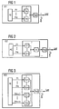
- FIG. 1 shows a first embodiment IS1 of an integrated circuit according to the invention, which has a programming unit PE, a driver T and a connection contact pad.
- a voltage U is present at the connection contact pad and a driver current I flows to the load, which is also designated.
- the driver T is equipped with several partial drivers T1..Tm connected in parallel, the outputs of which are all connected to a common connection contact pad and which can be activated with the aid of programming signals P1 ... Pm from a programming unit PE as required.
- a deactivated partial driver has a high resistance at its output.
- the total driver strength I of the driver T is the sum of the driver strengths I1 + I2 ... of all activated partial drivers T1, T2 ...
- the driver strengths of the individual sub-drivers do not have to be equally distributed.
- FIG. 2 shows a second embodiment IS2 of an integrated circuit according to the invention, which essentially differs from the embodiment IS1 shown in FIG. 1 only in that the driver T with only one output stage A and a plurality of control units S1 ... connected upstream of the output stage. Sm is equipped, the output of the output stage A being connected to the connection contact pad and the respective inputs of the respective control units being able to be activated as required via programming signals P1 ... Pm from a programming unit PE.
- the dimensioning of A essentially determines the static driver strength I, the dimensioning of the control units, however, the edge steepness dU / dt.
- the slope of the driver T can be set accordingly by connecting several controls S1..Sm in parallel.
- FIG. 3 shows a third embodiment IS3 of an integrated circuit according to the invention, which essentially differs from the embodiment IS1 in FIG. 1 in that the driver T via partial drivers TU1 ... TUm for charging the load and partial driver TD1 ... TDn for unloading the load, whereby the positive and negative edge of the output signal can be optimized separately with regard to EMC.
- the partial drivers TU1 ... TUm are activated or deactivated by the programming signals P1 ... Pm and the partial drivers TD1 ... TDm by further programming signals Pm + 1 ... Pm + n.
- the programming of the programming unit PE can already be done by the manufacturer of the integrated circuit, e.g. as mask-programmable ROM, or, as indicated in FIGS. 4 and 5, carried out by the board developer.
- FIG. 4 shows a fourth embodiment IS4 of an integrated circuit according to the invention, which essentially differs from embodiment 1 in that a programming bit PB for programming the programming unit PE can be fed to the programming unit PE via the connection contact pad and in that the programming unit PE has a Control signal PR can be controlled from a control register flag or an additional connection pin.
- PR 1
- FIG. 5 shows a fifth embodiment IS5 of an integrated circuit according to the invention, which essentially differs from the embodiment IS4 in that at least one respective additional driver T is provided, which is also controlled with the programming signals P1..Pm, which is controlled with at least a further connection contact pad is connected and which, however, has no connection between the connection contact pad and the programming unit PE.
- the dynamic output signals e.g. B. addresses or data
- only a subset of all drivers needs a programming unit. If the load conditions of an address or data bus are similar for all lines, all associated pad drivers can be programmed in the same way with regard to EMC.
- the programming bit PB can optionally be supplied from any of the connection contacts pad.
- FIG. 6 shows a sixth embodiment IS6 of an integrated circuit according to the invention, which represents a combination of the drivers shown in the previous figures, with pad driver T without an associated programming unit PE, different pad drivers T with a separate programming unit and groups of pad modules. Drivers with a common programming unit are available. This makes different programming signals PR1 ..PR3 necessary.
- the programming unit PE is integrated on an integrated circuit according to the invention, for example in the pad frame, where there are often gaps.
- the programming unit PE stores the logical state of the programming signals, since these must be applied statically to the partial drivers so that their scaling does not change during operation.
- the programming signals can be stored in a volatile memory, for example in a RAM or a flip-flop, or else in a non-volatile memory, such as in a ROM, OTP, EEPROM or fuse.
Abstract
Description
Um die Elektromagnetische Verträglichkeit (EMV) integrierter Schaltungen zu erhöhen, müssen die Pad-Treiber (Anschlußkontakt-Treiber) von integrierten Schaltungen auf die äußere Last angepaßt werden, um beispielsweise ![]()
![]()
Beispielsweise aus dem Paper 33.3 zur 28th ACM/IEEE Design Automation Conference, Seiten 567 bis 572 wird deutlich, daß es den EMV-optimalen Treiber für alle Lastfälle nicht gibt. Vielmehr hängt die Signalform sowohl von der Dimensionierung, insbesondere von der Treiberstärke I in Ampere und der Flankensteilheit dU/dt in V/sec, des Treibers ab als auch von der Art der Last, beispielsweise einer kapazitiven Last , einer offenen Leitung oder einem Leitungsnetz. Da eine integrierte Schaltung im allgemeinen nicht nur für eine bestimmte Anwendung mit klar definierter Lastumgebung eingesetzt wird, ist eine EMV-optimale Dimensionierung der Pad-Treiber nur anwendungsspezifisch möglich.For example, from paper 33.3 for the 28th ACM / IEEE Design Automation Conference, pages 567 to 572, it becomes clear that the EMC-optimal driver is not available for all load cases. Rather, the signal form depends both on the dimensioning, in particular on the driver strength I in amperes and the slope dU / dt in V / sec, of the driver and on the type of load, for example a capacitive load, an open line or a line network. Since an integrated circuit is generally not only used for a specific application with a clearly defined load environment, EMC-optimal dimensioning of the pad drivers is only possible for specific applications.
Aus der deutschen Patentschrift DE 44 41 523 C1 ist eine digitale Treiberschaltung für integrierte Schaltung bekannt, die an eine Lastkapazität durch Zuschalten entsprechend vieler Ausgangszweige angepaßt werden kann. Die Treiberschaltung ist vergleichsweise aufwendig, da neben den Ausgangszweigen Steuermittel zum Ansteuern der Ausgangszweige, eine Eingabevorrichtung zum Eingeben einer Maßzahl, ein Einstellmittel zum Ermitteln einer bestimmten Ausgangszweige zugeordneten Stellgroße aufgrund der Meßzahl und ein Schaltmittel zum Freigeben der bestimmten Ausgangszweige vorgesehen sind.From the German patent DE 44 41 523 C1 a digital driver circuit for integrated circuit is known which can be adapted to a load capacitance by connecting a corresponding number of output branches. The driver circuit is comparatively complex since, in addition to the output branches, control means for actuating the output branches, an input device for entering a measurement number, a setting means for determining a manipulated variable assigned to a specific output branch on the basis of the measurement number and a switching means for releasing the specific output branches are provided.
Ferner ist aus der deutschen Offenlegungsschrift DE 42 00 680 A1 eine Treiberschaltung bekannt, bei der durch eine Mehrzahl von Teiltreibern die Flankensteilheit der positiven und negativen Signalflanken getrennt eingestellt wird.Furthermore, a driver circuit is known from German published patent application DE 42 00 680 A1, in which a plurality of drivers are used the slope of the positive and negative signal edges is set separately by partial drivers.
Die der Erfindung zugrunde liegende Aufgabe besteht nun darin, eine Integrierte Schaltung mit einem Pad-Treiber anzugeben, dessen Treibereigenschaften, wie zum Beispiel Treiberstärke I in Ampere und der Flankensteilheit dU/dt in V/sec, an eine jeweilige äußere Last flexibel angepaßt werden kann, wobei hierfür eine möglichst geringe zusätzliche Chipfläche anzustreben ist.The object on which the invention is based is to provide an integrated circuit with a pad driver, the driver properties of which, such as driver strength I in amperes and the slope steepness dU / dt in V / sec, can be flexibly adapted to a respective external load , for which the smallest possible additional chip area should be aimed for.
Diese Aufgabe wird erfindungsgemäß durch die Merkmale des Patentanspruchs 1 gelöst. Vorteilhafte Ausgestaltungen der Erfindung ergeben sich aus den Unteransprüchen.This object is achieved by the features of
Die Erfindung wird nachfolgend anhand der Zeichnungen näher erläutert. Dabei zeigt
Figur 1- ein Blockschaltbild einer ersten Ausgestaltung der Erfindung,
- Figur 2
- ein Blockschaltbild einer zweiten Ausgestaltung der Erfindung,
- Figur 3
- ein Blockschaltbild einer dritten Ausgestaltung der Erfindung,
- Figur 4
- ein Blockschaltbild einer vierten Ausgestaltung der Erfindung,
- Figur 5
- ein Blockschaltbild einer fünften Ausgestaltung der Erfindung und
- Figur 6
- ein Blockschaltbild einer Kombination verschiedener Ausgestaltungen der Erfindung.
- Figure 1
- 2 shows a block diagram of a first embodiment of the invention,
- Figure 2
- 2 shows a block diagram of a second embodiment of the invention,
- Figure 3
- 2 shows a block diagram of a third embodiment of the invention,
- Figure 4
- 2 shows a block diagram of a fourth embodiment of the invention,
- Figure 5
- a block diagram of a fifth embodiment of the invention and
- Figure 6
- a block diagram of a combination of different embodiments of the invention.
In Figur 1 ist eine erste Ausgestaltung IS1 einer erfindungsgemäßen integrierten Schaltung dargestellt, die eine Programmiereinheit PE, einem Treiber T und einem Anschlußkontakt Pad aufweist. Am Anschlußkontakt Pad liegt dabei eine Spannung U an und es fließt ein Treiberstrom I zur ebenso bezeichneten Last. Der Treiber T ist mit mehreren parallelgeschalteten Teil-Treibern T1..Tm ausgestattet, deren Ausgänge alle mit einem gemeinsamen Anschlußkontakt Pad verbunden sind und die mit Hilfe von Programmiersignalen P1...Pm aus einer Programmiereinheit PE je nach Bedarf aktivierbar sind. Ein deaktivierter Teil-Treiber ist an seinem Ausgang hochohmig. Die Gesamttreiberstarke I des Treibers T ist die Summe der Treiberstarken I1 + I2... aller aktivierten Teil-Treiber T1, T2 .. . Die Treiberstarken der einzelnen Teil-Treiber müssen dabei nicht gleichverteilt sein.FIG. 1 shows a first embodiment IS1 of an integrated circuit according to the invention, which has a programming unit PE, a driver T and a connection contact pad. A voltage U is present at the connection contact pad and a driver current I flows to the load, which is also designated. The driver T is equipped with several partial drivers T1..Tm connected in parallel, the outputs of which are all connected to a common connection contact pad and which can be activated with the aid of programming signals P1 ... Pm from a programming unit PE as required. A deactivated partial driver has a high resistance at its output. The total driver strength I of the driver T is the sum of the driver strengths I1 + I2 ... of all activated partial drivers T1, T2 ... The driver strengths of the individual sub-drivers do not have to be equally distributed.
In Figur 2 ist eine zweite Ausgestaltung IS2 einer erfindungsgemäßen integrierten Schaltung dargestellt, die sich von der in Figur 1 dargestellten Ausgestaltung IS1 im wesentlichen nur dadurch unterscheidet, daß der Treiber T mit nur einer Ausgangsstufe A und einer Mehrzahl der Ausgangsstufe vorgeschalteten Ansteuereinheiten S1...Sm ausgestattet ist, wobei der Ausgang der Ausgangsstufe A mit dem Anschlußkontakt Pad verbunden ist und wobei die jeweiligen Eingange der jeweiligen Ansteuereinheiten über Programmiersignale P1...Pm aus einer Programmiereinheit PE je nach Bedarf aktivierbar sind. Die Dimensionierung von A bestimmt dabei im wesentlichen die statische Treiberstärke I, die Dimensionierung der Ansteuereinheiten hingegen die Flankensteilheit dU/dt. Entsprechend läßt sich die Flankensteilheit des Treibers T über die Parallelschaltung mehrerer Ansteuerungen S1..Sm einstellen.FIG. 2 shows a second embodiment IS2 of an integrated circuit according to the invention, which essentially differs from the embodiment IS1 shown in FIG. 1 only in that the driver T with only one output stage A and a plurality of control units S1 ... connected upstream of the output stage. Sm is equipped, the output of the output stage A being connected to the connection contact pad and the respective inputs of the respective control units being able to be activated as required via programming signals P1 ... Pm from a programming unit PE. The dimensioning of A essentially determines the static driver strength I, the dimensioning of the control units, however, the edge steepness dU / dt. The slope of the driver T can be set accordingly by connecting several controls S1..Sm in parallel.
In Figur 3 ist eine dritte Ausgestaltung IS3 einer erfindungsgemäßen integrierten Schaltung dargestellt, die sich von der in Figur 1 Ausgestaltung IS1 im wesentlichen dadurch unterscheidet, daß der Treiber T über Teil-Treiber TU1...TUm für das Aufladen der Last und Teil-Treiber TD1...TDn für das Entladen der Last verfügt, wodurch sich die positive und negative Flanke des Ausgangssignals getrennt voneinander hinsichtlich der EMV optimieren läßt. Die Teil-Treiber TU1...TUm werden dabei durch die Programmiersignale P1...Pm und die Teil-Treiber TD1...TDm durch weitere Programmiersignale Pm+1 ... Pm+n aktiviert bzw. deaktiviert.FIG. 3 shows a third embodiment IS3 of an integrated circuit according to the invention, which essentially differs from the embodiment IS1 in FIG. 1 in that the driver T via partial drivers TU1 ... TUm for charging the load and partial driver TD1 ... TDn for unloading the load, whereby the positive and negative edge of the output signal can be optimized separately with regard to EMC. The partial drivers TU1 ... TUm are activated or deactivated by the programming signals P1 ... Pm and the partial drivers TD1 ... TDm by further programming signals Pm + 1 ... Pm + n.
Darüberhinaus sind beliebige Kombinationen der Merkmale der ersten bis dritten Ausgestaltung möglich.In addition, any combinations of the features of the first to third embodiments are possible.
Die Programmierung der Programmiereinheit PE kann bereits vom Hersteller der integrierten Schaltung, z.B. als maskenprogrammierbares ROM, oder aber, wie in Figur 4 und 5 angedeutet, vom Platinenentwickler durchgeführt werden.The programming of the programming unit PE can already be done by the manufacturer of the integrated circuit, e.g. as mask-programmable ROM, or, as indicated in FIGS. 4 and 5, carried out by the board developer.
In Figur 4 ist eine vierte Ausgestaltung IS4 einer erfindungsgemäßen integrierten Schaltung dargestellt, die sich von der Ausgestaltung 1 im wesentlichen dadurch unterscheidet, daß ein Programmierbit PB zur Programmierung der Programmiereinheit PE über den Anschlußkontakt Pad der Programmiereinheit PE zuführbar ist und daß die Programmiereinheit PE durch ein Steuersignal PR aus einem Steuerregister Flag oder einem zusätzlichen Anschluß Pin ansteuerbar ist.FIG. 4 shows a fourth embodiment IS4 of an integrated circuit according to the invention, which essentially differs from
Damit die Programmierung vom Platinenentwickler durchführbar ist, muß der Treiber einen Programmier-Modus unterstützen. Betrachtet man zunächst nur die Programmierung eines einzelnen Pad-Treibers, so kann der Programmier-Modus durch das Steuersignal PR eingeleitet werden. Fur z. B. PR = 1 übernimmt die Programmiereinheit PE das erste Programmierbit PB über den Anschlußkontakt Pad. Gleichzeitig deaktivieren die Programmiersignale P1..Pm den Treiber T. Danach wird PR = 0. Beim nächsten PR = 1 wird das nächste Programmierbit nach PE übertragen. Ein besonderer Vorteil liegt hier in der flächensparenden Programmiermethode.The driver must support a programming mode so that the programming can be carried out by the board developer. If you first consider only the programming of a single pad driver, the programming mode can be initiated by the control signal PR. For z. B. PR = 1, the programming unit PE takes over the first programming bit PB via the connection pad. At the same time, the programming signals P1..Pm deactivate the driver T. Then PR = 0. At the next PR = 1, the next programming bit is transferred to PE. A particular advantage here is the space-saving programming method.
In Figur 5 ist eine fünfte Ausgestaltung IS5 eine erfindungsgemäßen integrierten Schaltung dargestellt, die sich von der Ausgestaltung IS4 im wesentlichen dadurch unterscheidet, daß mindestens ein jeweiliger weiterer Treiber T vorgesehen ist, der ebenso mit den Programmiersignalen P1..Pm angesteuert wird, der mit mindestens einem weiteren Anschlußkontakt Pad verbunden ist und der jedoch keine Verbindung zwischen dem Anschlußkontakt Pad und der Programmiereinheit PE aufweist. Da nur diejenigen Pad-Treiber der integrierten Schaltung auf EMV optimierbar sein müssen, die dynamische Ausgangssignale, z. B. Adressen oder Daten, treiben, braucht nur eine Untermenge aller Treiber eine Programmiereinheit. Sind die Lastverhältnisse eines Adreß- oder Datenbusses für alle Leitungen ähnlich, so können alle zugehörigen Pad-Treiber hinsichtlich der EMV gleichartig programmiert werden. Das Programmierbit PB kann dabei wahlweise von irgend einem der Anschlußkontakte Pad zugeführt werden.FIG. 5 shows a fifth embodiment IS5 of an integrated circuit according to the invention, which essentially differs from the embodiment IS4 in that at least one respective additional driver T is provided, which is also controlled with the programming signals P1..Pm, which is controlled with at least a further connection contact pad is connected and which, however, has no connection between the connection contact pad and the programming unit PE. Since only those pad drivers of the integrated circuit must be able to be optimized for EMC, the dynamic output signals, e.g. B. addresses or data, only a subset of all drivers needs a programming unit. If the load conditions of an address or data bus are similar for all lines, all associated pad drivers can be programmed in the same way with regard to EMC. The programming bit PB can optionally be supplied from any of the connection contacts pad.
In Figur 6 ist eine sechste Ausgestaltung IS6 einer erfindungsgemäßen integrierten Schaltung dargestellt, die eine Kombination aus den in den vorhergehenden Figuren gezeigten Treibern darstellt, wobei Pad-Treiber T ohne zugehörige Programmiereinheit PE, verschiedene Pad-Treiber T mit getrennter Programmiereinheit und Gruppen von Pad-Treibern mit gemeinsamer Programmiereinheit vorhanden sind. Dies macht unterschiedliche Programmiersignale PR1 ..PR3 notwendig.FIG. 6 shows a sixth embodiment IS6 of an integrated circuit according to the invention, which represents a combination of the drivers shown in the previous figures, with pad driver T without an associated programming unit PE, different pad drivers T with a separate programming unit and groups of pad modules. Drivers with a common programming unit are available. This makes different programming signals PR1 ..PR3 necessary.
Die Programmiereinheit PE ist auf einer erfindungsgemäßen integrierten Schaltung, zum Beispiel im Pad-Rahmen, wo oft Lükken sind, integriert. Die Programmiereinheit PE speichert den logischen Zustand der Programmiersignale, da diese statisch an den Teil-Treibern anliegen müssen, damit sich deren Skalierung während des Betriebs nicht ändert. Die Speicherung der Programmiersignale kann in einem flüchtigen Speicher, zum Beispiel in einem RAM oder einem Flip-Flop, oder aber in einem nicht-flüchtigen Speicher, wie beispielsweise einem ROM, OTP, EEPROM oder Fuse erfolgen.The programming unit PE is integrated on an integrated circuit according to the invention, for example in the pad frame, where there are often gaps. The programming unit PE stores the logical state of the programming signals, since these must be applied statically to the partial drivers so that their scaling does not change during operation. The programming signals can be stored in a volatile memory, for example in a RAM or a flip-flop, or else in a non-volatile memory, such as in a ROM, OTP, EEPROM or fuse.
EMV-Regeln für die Programmierung der Programmiereinheit PE:EMC rules for programming the programming unit PE:
Um den Störeinfluß von Signalen möglichst gering zu halten, müssen schnelle unerwünschte Amplitudenänderungen, die durch Leitungsreflektionen entstehen, so gut wie möglich verhindert werden.
- a) Durch die Dimensionierung der Treiberstärke (in Ampere) bei vorgegebener Betriebsspannung (in Volt) kann der Innenwiderstand der Signalquelle eingestellt werden. Es ist anzustreben, daß der differentielle Innenwiderstand der statischen Ausgangskennlinien des Treibers sowohl für den "LOW" als auch den "HIGH" Pegel dem Wellenwiderstand der angeschlossenen Leitung entspricht.
Durch diese Maßnahme werden Reflektionen an der Signalquelle vermieden. - b) Durch die Dimensionierung der Flankensteilheit (in Volt/Sekunde) kann der Einfluß der am Leitungsende entstehenden Reflektionen eingestellt werden. Es ist anzustreben, daß eine von einem Treiber angesteuerte Leitung "elektrisch kurz" ist. Dies wird erzielt, wenn die erste am Leitungsende reflektierte Welle den Sender wieder erreicht, wenn die Anstiegs-/Abfallflanke ihren Endwert noch nicht erreicht hat. In diesem Fall wird die (am Leitungsende angeregte) Reflektion durch den Sender dominiert und abgeschwächt. Daraus ergibt sich die Regel: Die Anstiegs-/Abfallzeit sollte größer sein, als die doppelte Verzögerungszeit der angeschlossenen Leitung.
- a) The internal resistance of the signal source can be set by dimensioning the driver strength (in amperes) for a given operating voltage (in volts). It is desirable to ensure that the differential internal resistance of the static output characteristics of the driver corresponds to the characteristic impedance of the connected line for both the "LOW" and the "HIGH" level.
This measure prevents reflections from the signal source. - b) By dimensioning the slope (in volts / second), the influence of the reflections occurring at the end of the line can be adjusted. It is desirable that a line driven by a driver be "electrically short". This is achieved when the first wave reflected at the end of the line reaches the transmitter again, when the rising / falling edge has not yet reached its end value. In this case, the reflection (excited at the end of the line) is dominated and weakened by the transmitter. This results in the rule: The rise / fall time should be greater than twice the delay time of the connected line.
Claims (5)
bei der eine bestimmte Treiberstarke und Flankensteilheit des Pad-Treibers dadurch einstellbar ist, daß abhängig von Ausgangssignalen (P1..Pm) der Programmiereinheit entsprechend viele ausgangsseitig mit einem gemeinsamen Anschlußkontakt (Pad) verbundene Teil-Treiber aktiviert/deaktiviert werden, bei der die Programmiereinheit einen Speicher aufweist, dessen Ausgangssignale die Ausgangssignale der Programmiereinheit darstellen und dessen serieller Eingang mit dem gemeinsamen Anschlußkontakt (Pad) verbunden ist, wobei abhängig von einem Steuersignal (PR) ein Programmierbit-Signal (PB) in den Speicher eingeschrieben wird, und
bei der die Programmiereinheit derart vorgesehen ist, daß aufgrund der Ausgangssignale der Programmiereinheit alle Teil-Treiber deaktiviert sind, während das Programmierbitsignal in den Speicher eingeschrieben wird.Integrated circuit with at least one pad driver, which has a programming unit (PE) and a plurality of partial drivers (T1..Tm),
in which a certain driver strength and edge steepness of the pad driver can be set by activating / deactivating, depending on the output signals (P1..Pm) of the programming unit, the corresponding number of partial drivers connected to a common connection contact (pad) on the output side, in which the programming unit has a memory whose output signals represent the output signals of the programming unit and whose serial input is connected to the common connection contact (pad), a programming bit signal (PB) being written into the memory as a function of a control signal (PR), and
in which the programming unit is provided in such a way that, based on the output signals of the programming unit, all sub-drivers are deactivated while the programming bit signal is being written into the memory.
bei der die Flankensteilheit einer positiven Signalflanke dadurch getrennt von der Flankensteilheit einer negativen Signalflanke eingestellt wird, daß ein erster Teil (TU1..TUm) der Mehrzahl von Teil-Treibern nur für die positve Signalflanke vorgesehen und durch erste Ausgangssignale (P1..Pm) der Programmiereinheit aktiviert/deaktiviert wird und daß ein zweiter Teil (TD1..TDn) der Mehrzahl von Teil-Treibern nur für die negative Signalflanke vorgesehen und durch erste Ausgangssignale (Pm+1..Pm+n) der Programmiereinheit aktiviert/deaktiviert wird,Integrated circuit according to Claim 1,
in which the edge steepness of a positive signal edge is set separately from the edge steepness of a negative signal edge in that a first part (TU1..TUm) of the plurality of part drivers is provided only for the positive signal edge and by first output signals (P1..Pm) the programming unit is activated / deactivated and that a second part (TD1..TDn) of the plurality of part drivers is provided only for the negative signal edge and is activated / deactivated by first output signals (Pm + 1..Pm + n) of the programming unit,
bei der in der integrierten Schaltung ein Register (Flag) vorgesehen ist an dessen Ausgang das Steuersignal anliegt.Integrated circuit according to Claim 1 or 2,
in which a register (flag) is provided in the integrated circuit, at whose output the control signal is present.
bei der das Steuersignal (PR) aber einen weiteren Anschlußkontakt (Pin) extern zugeführt wird.Integrated circuit according to Claim 1 or 2,
in which the control signal (PR) but an additional connection contact (pin) is supplied externally.
bei der mindestens ein weiter Pad-Treiber (T1) vorgesehen ist, der gemeinsam mit dem jeweiligen Pad-Treiber (T) durch durch die Ausgangssignale (P1..Pm) der jeweiligen Programmiereinheit (PE) angesteuert wird.Integrated circuit according to one of the preceding claims,
in which at least one further pad driver (T1) is provided, which is controlled together with the respective pad driver (T) by the output signals (P1..Pm) of the respective programming unit (PE).
Applications Claiming Priority (2)
| Application Number | Priority Date | Filing Date | Title |
|---|---|---|---|
| DE19545904 | 1995-12-08 | ||
| DE19545904A DE19545904C2 (en) | 1995-12-08 | 1995-12-08 | Integrated circuit with programmable pad driver |
Publications (2)
| Publication Number | Publication Date |
|---|---|
| EP0778673A1 true EP0778673A1 (en) | 1997-06-11 |
| EP0778673B1 EP0778673B1 (en) | 2000-05-24 |
Family
ID=7779606
Family Applications (1)
| Application Number | Title | Priority Date | Filing Date |
|---|---|---|---|
| EP96118287A Expired - Lifetime EP0778673B1 (en) | 1995-12-08 | 1996-11-14 | Integrated circuit with programmable pad-driver |
Country Status (3)
| Country | Link |
|---|---|
| US (1) | US5834955A (en) |
| EP (1) | EP0778673B1 (en) |
| DE (2) | DE19545904C2 (en) |
Cited By (2)
| Publication number | Priority date | Publication date | Assignee | Title |
|---|---|---|---|---|
| EP0913943A2 (en) * | 1997-10-29 | 1999-05-06 | Hewlett-Packard Company | Integrated circuit assembly having output pads with programmable characteristics and method of operation |
| DE19841757C1 (en) * | 1998-09-11 | 2000-03-02 | Siemens Ag | Output driver output signal matching circuit for integrated circuit meeting required output signal slope |
Families Citing this family (11)
| Publication number | Priority date | Publication date | Assignee | Title |
|---|---|---|---|---|
| JP3369807B2 (en) | 1995-08-30 | 2003-01-20 | 株式会社東芝 | Semiconductor device |
| DE19901460C1 (en) | 1999-01-15 | 2000-08-31 | Siemens Ag | Integrated semiconductor circuit and method for checking the transmission behavior of pad cells |
| US6271699B1 (en) | 1999-04-02 | 2001-08-07 | Motorola, Inc. | Driver circuit and method for controlling transition time of a signal |
| US6483879B1 (en) | 1999-08-27 | 2002-11-19 | Lsi Logic Corporation | Compensating for initial signal interference exhibited by differential transmission lines |
| DE10036863C2 (en) * | 2000-07-28 | 2002-09-19 | Texas Instruments Deutschland | Driver circuit for delivering an adjustable output signal current |
| US7132868B2 (en) | 2001-06-27 | 2006-11-07 | Mitsubishi Denki Kabushiki Kaisha | Semiconductor device |
| DE10148338B4 (en) * | 2001-09-29 | 2005-11-10 | Infineon Technologies Ag | Scalable driver device and associated integrated circuit |
| KR100567077B1 (en) | 2005-01-31 | 2006-04-04 | 주식회사 하이닉스반도체 | Memory device with a device for re-calibrating the output of an internal circuit and the method for re-calibrating the output signal |
| DE102008017161B4 (en) * | 2008-04-03 | 2012-05-31 | Continental Automotive Gmbh | Device for operating a circuit arrangement |
| US8282435B2 (en) * | 2009-03-09 | 2012-10-09 | Topanga Technologies, Inc. | Method and system for replacing a plasma lamp from a resonator assembly |
| US8731002B2 (en) * | 2011-03-25 | 2014-05-20 | Invensense, Inc. | Synchronization, re-synchronization, addressing, and serialized signal processing for daisy-chained communication devices |
Citations (7)
| Publication number | Priority date | Publication date | Assignee | Title |
|---|---|---|---|---|
| US4697107A (en) * | 1986-07-24 | 1987-09-29 | National Semiconductor Corporation | Four-state I/O control circuit |
| EP0315473A2 (en) * | 1987-11-05 | 1989-05-10 | Texas Instruments Incorporated | Output buffer having programmable drive current |
| EP0463316A1 (en) * | 1990-06-07 | 1992-01-02 | International Business Machines Corporation | Self-adjusting impedance matching driver |
| DE4200680A1 (en) | 1992-01-14 | 1993-07-15 | Bosch Gmbh Robert | DRIVER CIRCUIT |
| DE4224804C1 (en) * | 1992-07-27 | 1994-01-13 | Siemens Ag | Programmable logic circuitry |
| US5294845A (en) * | 1990-12-24 | 1994-03-15 | Motorola, Inc. | Data processor having an output terminal with selectable output impedances |
| DE4441523C1 (en) | 1994-11-22 | 1996-05-15 | Itt Ind Gmbh Deutsche | Digital driver circuit for an integrated circuit |
Family Cites Families (7)
| Publication number | Priority date | Publication date | Assignee | Title |
|---|---|---|---|---|
| DK158168C (en) * | 1985-06-19 | 1990-09-17 | Risoe Forsoegsanlaeg | CONNECTION TO PROCESSING SIGNALS FROM A NUCLEAR DETECTOR |
| US5170073A (en) * | 1991-10-24 | 1992-12-08 | Intel Corporation | Ultra-low noise port output driver circuit |
| JP3131931B2 (en) * | 1992-03-13 | 2001-02-05 | 日本電信電話株式会社 | High frequency high power amplifier |
| US5682116A (en) * | 1994-06-07 | 1997-10-28 | International Business Machines Corporation | Off chip driver having slew rate control and differential voltage protection circuitry |
| JP3064842B2 (en) * | 1995-01-04 | 2000-07-12 | 日本電気株式会社 | Drive circuit |
| US5600271A (en) * | 1995-09-15 | 1997-02-04 | Xilinx, Inc. | Input signal interface with independently controllable pull-up and pull-down circuitry |
| US5703496A (en) * | 1995-09-26 | 1997-12-30 | Intel Corporation | Method and apparatus for limiting the slew rate of output drivers by selectively programming the threshold voltage of flash cells connected thereto |
-
1995
- 1995-12-08 DE DE19545904A patent/DE19545904C2/en not_active Expired - Fee Related
-
1996
- 1996-11-14 DE DE59605299T patent/DE59605299D1/en not_active Expired - Lifetime
- 1996-11-14 EP EP96118287A patent/EP0778673B1/en not_active Expired - Lifetime
- 1996-12-04 US US08/752,372 patent/US5834955A/en not_active Expired - Lifetime
Patent Citations (7)
| Publication number | Priority date | Publication date | Assignee | Title |
|---|---|---|---|---|
| US4697107A (en) * | 1986-07-24 | 1987-09-29 | National Semiconductor Corporation | Four-state I/O control circuit |
| EP0315473A2 (en) * | 1987-11-05 | 1989-05-10 | Texas Instruments Incorporated | Output buffer having programmable drive current |
| EP0463316A1 (en) * | 1990-06-07 | 1992-01-02 | International Business Machines Corporation | Self-adjusting impedance matching driver |
| US5294845A (en) * | 1990-12-24 | 1994-03-15 | Motorola, Inc. | Data processor having an output terminal with selectable output impedances |
| DE4200680A1 (en) | 1992-01-14 | 1993-07-15 | Bosch Gmbh Robert | DRIVER CIRCUIT |
| DE4224804C1 (en) * | 1992-07-27 | 1994-01-13 | Siemens Ag | Programmable logic circuitry |
| DE4441523C1 (en) | 1994-11-22 | 1996-05-15 | Itt Ind Gmbh Deutsche | Digital driver circuit for an integrated circuit |
Cited By (3)
| Publication number | Priority date | Publication date | Assignee | Title |
|---|---|---|---|---|
| EP0913943A2 (en) * | 1997-10-29 | 1999-05-06 | Hewlett-Packard Company | Integrated circuit assembly having output pads with programmable characteristics and method of operation |
| EP0913943A3 (en) * | 1997-10-29 | 2000-02-02 | Hewlett-Packard Company | Integrated circuit assembly having output pads with programmable characteristics and method of operation |
| DE19841757C1 (en) * | 1998-09-11 | 2000-03-02 | Siemens Ag | Output driver output signal matching circuit for integrated circuit meeting required output signal slope |
Also Published As
| Publication number | Publication date |
|---|---|
| EP0778673B1 (en) | 2000-05-24 |
| US5834955A (en) | 1998-11-10 |
| DE19545904C2 (en) | 1998-01-15 |
| DE19545904A1 (en) | 1997-06-12 |
| DE59605299D1 (en) | 2000-06-29 |
Similar Documents
| Publication | Publication Date | Title |
|---|---|---|
| EP0090255B1 (en) | Tristate driver circuit | |
| DE3520003C2 (en) | ||
| DE3215671C2 (en) | Programmable logic arrangement | |
| EP0778673B1 (en) | Integrated circuit with programmable pad-driver | |
| DE3901636A1 (en) | DATA INPUT ARRANGEMENT WITH MICROCALCULATOR | |
| DE4207999A1 (en) | ADDRESS INPUT BUFFER DEVICE | |
| DE3727035C2 (en) | ||
| DE10142840B4 (en) | delay circuit | |
| DE2643020A1 (en) | SCHMITT TRIGGER | |
| DE4324138B4 (en) | CMOS tri-state buffer circuit | |
| EP0203535B1 (en) | Method for fault simulation in a logic circuit and circuit arrangement for carrying it out | |
| EP0061513B1 (en) | Cmos integrated selection circuit for four potentials and simplifications of it for three potentials | |
| EP0186040A1 (en) | Integrated semiconductor memory | |
| DE4420988A1 (en) | Method for testing an integrated circuit and integrated circuit arrangement with a test circuit | |
| EP0214508A2 (en) | Integrated semiconducteur memory | |
| DE2131939C3 (en) | Logically controlled inverter stage | |
| EP0733910B1 (en) | Printed circuit board with built-in testing of connections to ICs | |
| DE3317295C2 (en) | Logic circuit with at least two pairs of input terminals | |
| EP0757254A2 (en) | Integrated circuit | |
| EP0368859B1 (en) | Programmable circuits | |
| DE2052519C3 (en) | Logical circuit | |
| DE3913216C2 (en) | ||
| EP0093899B1 (en) | Circuit for matching test equipment with a test piece | |
| EP0588111B1 (en) | Memory element | |
| EP0985271A1 (en) | Input circuit for an integrated circuit |
Legal Events
| Date | Code | Title | Description |
|---|---|---|---|
| PUAI | Public reference made under article 153(3) epc to a published international application that has entered the european phase |
Free format text: ORIGINAL CODE: 0009012 |
|
| AK | Designated contracting states |
Kind code of ref document: A1 Designated state(s): DE FR GB IT |
|
| 17P | Request for examination filed |
Effective date: 19971120 |
|
| 17Q | First examination report despatched |
Effective date: 19980120 |
|
| GRAG | Despatch of communication of intention to grant |
Free format text: ORIGINAL CODE: EPIDOS AGRA |
|
| GRAG | Despatch of communication of intention to grant |
Free format text: ORIGINAL CODE: EPIDOS AGRA |
|
| GRAH | Despatch of communication of intention to grant a patent |
Free format text: ORIGINAL CODE: EPIDOS IGRA |
|
| GRAH | Despatch of communication of intention to grant a patent |
Free format text: ORIGINAL CODE: EPIDOS IGRA |
|
| GRAA | (expected) grant |
Free format text: ORIGINAL CODE: 0009210 |
|
| AK | Designated contracting states |
Kind code of ref document: B1 Designated state(s): DE FR GB IT |
|
| REF | Corresponds to: |
Ref document number: 59605299 Country of ref document: DE Date of ref document: 20000629 |
|
| ITF | It: translation for a ep patent filed |
Owner name: STUDIO JAUMANN P. & C. S.N.C. |
|
| GBT | Gb: translation of ep patent filed (gb section 77(6)(a)/1977) |
Effective date: 20000727 |
|
| ET | Fr: translation filed | ||
| PLBE | No opposition filed within time limit |
Free format text: ORIGINAL CODE: 0009261 |
|
| STAA | Information on the status of an ep patent application or granted ep patent |
Free format text: STATUS: NO OPPOSITION FILED WITHIN TIME LIMIT |
|
| 26N | No opposition filed | ||
| REG | Reference to a national code |
Ref country code: GB Ref legal event code: IF02 |
|
| REG | Reference to a national code |
Ref country code: GB Ref legal event code: 732E Free format text: REGISTERED BETWEEN 20110707 AND 20110713 |
|
| REG | Reference to a national code |
Ref country code: FR Ref legal event code: TP Owner name: INFINEON TECHNOLOGIES AG, DE Effective date: 20110922 |
|
| REG | Reference to a national code |
Ref country code: DE Ref legal event code: R081 Ref document number: 59605299 Country of ref document: DE Owner name: INFINEON TECHNOLOGIES AG, DE Free format text: FORMER OWNER: SIEMENS AKTIENGESELLSCHAFT, 80333 MUENCHEN, DE Effective date: 20111107 |
|
| REG | Reference to a national code |
Ref country code: FR Ref legal event code: PLFP Year of fee payment: 20 |
|
| PGFP | Annual fee paid to national office [announced via postgrant information from national office to epo] |
Ref country code: IT Payment date: 20151125 Year of fee payment: 20 Ref country code: GB Payment date: 20151118 Year of fee payment: 20 |
|
| PGFP | Annual fee paid to national office [announced via postgrant information from national office to epo] |
Ref country code: FR Payment date: 20151119 Year of fee payment: 20 |
|
| PGFP | Annual fee paid to national office [announced via postgrant information from national office to epo] |
Ref country code: DE Payment date: 20160115 Year of fee payment: 20 |
|
| REG | Reference to a national code |
Ref country code: DE Ref legal event code: R071 Ref document number: 59605299 Country of ref document: DE |
|
| REG | Reference to a national code |
Ref country code: GB Ref legal event code: PE20 Expiry date: 20161113 |
|
| PG25 | Lapsed in a contracting state [announced via postgrant information from national office to epo] |
Ref country code: GB Free format text: LAPSE BECAUSE OF EXPIRATION OF PROTECTION Effective date: 20161113 |