EP0776032A2 - Plasma-Ätz-Verfahren - Google Patents
Plasma-Ätz-Verfahren Download PDFInfo
- Publication number
- EP0776032A2 EP0776032A2 EP96117162A EP96117162A EP0776032A2 EP 0776032 A2 EP0776032 A2 EP 0776032A2 EP 96117162 A EP96117162 A EP 96117162A EP 96117162 A EP96117162 A EP 96117162A EP 0776032 A2 EP0776032 A2 EP 0776032A2
- Authority
- EP
- European Patent Office
- Prior art keywords
- etching
- gas
- layer
- charaterized
- plasma
- Prior art date
- Legal status (The legal status is an assumption and is not a legal conclusion. Google has not performed a legal analysis and makes no representation as to the accuracy of the status listed.)
- Granted
Links
- 238000000034 method Methods 0.000 title claims abstract description 139
- 238000001020 plasma etching Methods 0.000 title claims abstract description 19
- 239000007789 gas Substances 0.000 claims abstract description 118
- 238000005530 etching Methods 0.000 claims abstract description 108
- 230000008569 process Effects 0.000 claims abstract description 101
- VYPSYNLAJGMNEJ-UHFFFAOYSA-N Silicium dioxide Chemical compound O=[Si]=O VYPSYNLAJGMNEJ-UHFFFAOYSA-N 0.000 claims abstract description 58
- 229920002120 photoresistant polymer Polymers 0.000 claims abstract description 16
- 239000012159 carrier gas Substances 0.000 claims abstract description 15
- 229910052710 silicon Inorganic materials 0.000 claims abstract description 5
- 229910052814 silicon oxide Inorganic materials 0.000 claims description 21
- 238000010494 dissociation reaction Methods 0.000 claims description 13
- 230000005593 dissociations Effects 0.000 claims description 13
- 239000000758 substrate Substances 0.000 claims description 10
- 229910052782 aluminium Inorganic materials 0.000 claims description 5
- 229910052786 argon Inorganic materials 0.000 claims description 5
- 229910008484 TiSi Inorganic materials 0.000 claims description 4
- ATJFFYVFTNAWJD-UHFFFAOYSA-N Tin Chemical compound [Sn] ATJFFYVFTNAWJD-UHFFFAOYSA-N 0.000 claims description 4
- 239000000463 material Substances 0.000 claims description 4
- 229910052734 helium Inorganic materials 0.000 claims description 3
- 230000010349 pulsation Effects 0.000 claims description 3
- PGFXOWRDDHCDTE-UHFFFAOYSA-N hexafluoropropylene oxide Chemical compound FC(F)(F)C1(F)OC1(F)F PGFXOWRDDHCDTE-UHFFFAOYSA-N 0.000 abstract description 29
- 229910052681 coesite Inorganic materials 0.000 abstract description 17
- 229910052906 cristobalite Inorganic materials 0.000 abstract description 17
- 239000000377 silicon dioxide Substances 0.000 abstract description 17
- 229910052682 stishovite Inorganic materials 0.000 abstract description 17
- 229910052905 tridymite Inorganic materials 0.000 abstract description 17
- XUIMIQQOPSSXEZ-UHFFFAOYSA-N Silicon Chemical compound [Si] XUIMIQQOPSSXEZ-UHFFFAOYSA-N 0.000 abstract description 3
- 239000010703 silicon Substances 0.000 abstract description 3
- 239000000203 mixture Substances 0.000 abstract description 2
- 235000012431 wafers Nutrition 0.000 description 27
- 239000010408 film Substances 0.000 description 19
- 238000001816 cooling Methods 0.000 description 12
- 238000009792 diffusion process Methods 0.000 description 9
- 239000002826 coolant Substances 0.000 description 6
- 239000000126 substance Substances 0.000 description 6
- 238000012546 transfer Methods 0.000 description 6
- 230000008021 deposition Effects 0.000 description 5
- 238000002474 experimental method Methods 0.000 description 4
- XAGFODPZIPBFFR-UHFFFAOYSA-N aluminium Chemical compound [Al] XAGFODPZIPBFFR-UHFFFAOYSA-N 0.000 description 3
- 230000003028 elevating effect Effects 0.000 description 3
- 150000002500 ions Chemical class 0.000 description 3
- 239000010453 quartz Substances 0.000 description 3
- 239000004065 semiconductor Substances 0.000 description 3
- 239000010409 thin film Substances 0.000 description 3
- XKRFYHLGVUSROY-UHFFFAOYSA-N Argon Chemical compound [Ar] XKRFYHLGVUSROY-UHFFFAOYSA-N 0.000 description 2
- 230000008901 benefit Effects 0.000 description 2
- 238000009835 boiling Methods 0.000 description 2
- 239000000919 ceramic Substances 0.000 description 2
- 229910021419 crystalline silicon Inorganic materials 0.000 description 2
- 230000003247 decreasing effect Effects 0.000 description 2
- -1 e.g. Substances 0.000 description 2
- 229910052731 fluorine Inorganic materials 0.000 description 2
- VBZWSGALLODQNC-UHFFFAOYSA-N hexafluoroacetone Chemical compound FC(F)(F)C(=O)C(F)(F)F VBZWSGALLODQNC-UHFFFAOYSA-N 0.000 description 2
- 239000011810 insulating material Substances 0.000 description 2
- 230000010354 integration Effects 0.000 description 2
- 230000009965 odorless effect Effects 0.000 description 2
- 239000011347 resin Substances 0.000 description 2
- 229920005989 resin Polymers 0.000 description 2
- IJGRMHOSHXDMSA-UHFFFAOYSA-N Atomic nitrogen Chemical compound N#N IJGRMHOSHXDMSA-UHFFFAOYSA-N 0.000 description 1
- 239000004642 Polyimide Substances 0.000 description 1
- 230000009471 action Effects 0.000 description 1
- 230000002457 bidirectional effect Effects 0.000 description 1
- 239000006227 byproduct Substances 0.000 description 1
- 238000006243 chemical reaction Methods 0.000 description 1
- 239000004020 conductor Substances 0.000 description 1
- 238000007796 conventional method Methods 0.000 description 1
- 238000013461 design Methods 0.000 description 1
- 229910001873 dinitrogen Inorganic materials 0.000 description 1
- 125000001153 fluoro group Chemical class F* 0.000 description 1
- 230000005484 gravity Effects 0.000 description 1
- 238000010438 heat treatment Methods 0.000 description 1
- 239000001307 helium Substances 0.000 description 1
- SWQJXJOGLNCZEY-UHFFFAOYSA-N helium atom Chemical compound [He] SWQJXJOGLNCZEY-UHFFFAOYSA-N 0.000 description 1
- 230000007246 mechanism Effects 0.000 description 1
- 238000002844 melting Methods 0.000 description 1
- 230000008018 melting Effects 0.000 description 1
- 239000004570 mortar (masonry) Substances 0.000 description 1
- 230000003647 oxidation Effects 0.000 description 1
- 238000007254 oxidation reaction Methods 0.000 description 1
- 230000000149 penetrating effect Effects 0.000 description 1
- 230000000704 physical effect Effects 0.000 description 1
- 229920001721 polyimide Polymers 0.000 description 1
- 238000012545 processing Methods 0.000 description 1
- 238000011268 retreatment Methods 0.000 description 1
- 231100000279 safety data Toxicity 0.000 description 1
- 238000007789 sealing Methods 0.000 description 1
Images

Classifications
-
- H—ELECTRICITY
- H01—ELECTRIC ELEMENTS
- H01L—SEMICONDUCTOR DEVICES NOT COVERED BY CLASS H10
- H01L21/00—Processes or apparatus adapted for the manufacture or treatment of semiconductor or solid state devices or of parts thereof
- H01L21/02—Manufacture or treatment of semiconductor devices or of parts thereof
- H01L21/04—Manufacture or treatment of semiconductor devices or of parts thereof the devices having potential barriers, e.g. a PN junction, depletion layer or carrier concentration layer
- H01L21/18—Manufacture or treatment of semiconductor devices or of parts thereof the devices having potential barriers, e.g. a PN junction, depletion layer or carrier concentration layer the devices having semiconductor bodies comprising elements of Group IV of the Periodic Table or AIIIBV compounds with or without impurities, e.g. doping materials
- H01L21/30—Treatment of semiconductor bodies using processes or apparatus not provided for in groups H01L21/20 - H01L21/26
- H01L21/31—Treatment of semiconductor bodies using processes or apparatus not provided for in groups H01L21/20 - H01L21/26 to form insulating layers thereon, e.g. for masking or by using photolithographic techniques; After treatment of these layers; Selection of materials for these layers
- H01L21/3105—After-treatment
- H01L21/311—Etching the insulating layers by chemical or physical means
- H01L21/31105—Etching inorganic layers
- H01L21/31111—Etching inorganic layers by chemical means
- H01L21/31116—Etching inorganic layers by chemical means by dry-etching
Definitions
- the present invention relates to a method of plasma-etching a target layer comprising silicon oxide, and a process gas used in the method.
- CD loss critical dimension loss
- a contact hole having a diameter of 0.3 ⁇ m and a high aspect ratio in a silicon-oxide-based layer, such as an SiO 2 film, which is widely used as an interlevel insulating film In this case, if an etching selection ratio of the silicon oxide film to a photoresist is low, a little CD loss is generated due to retreatment of the photoresist, so that the yield is greatly affected.
- etching apparatuses for processing the substrates one by one have become the main current, in order to perform a uniform and fine process.
- the etching apparatuses of the above described one-by-one type require a high etching rate, so that a high throughput is obtained.
- the etching apparatuses currently used are constituted such that plasma of a high density is generated in a process chamber, thereby ensuring a high etching rate.
- Gases based on CxFy are generally used as an etching gas for plasma-etching a silicon-oxide-based layer, such as an SiO 2 film.
- a gas, in which x : y 1 : 2, such as C 4 F 8 gas, is representative, since such a gas provides an excellent balance between a high etching selection ratio and a high etching rate. If the ratio between C and F in an etching gas is deviated from an optimum value, the etching ratio may be decreased, or the etching rate is decreased due to an amount of by-product deposition, such as carbide.
- the C 4 F 8 gas is generally used under a low pressure of less than 10 mTorr, so that it is difficult to control the dissociation of the gas. As a result, problems are apt to occur such that fluorine-contained radicals are produced excessively so as to decrease the etching selection ratio, or fluorine-contained radicals are insufficient so as to cause a deposition to adhere and decrease the etching rate. Further, the etching rate and the aspect ratio presented by the C 4 F 8 gas are not satisfactory in consideration of a high throughput and a high degree of integration level currently required, even if the C 4 F 8 gas is accurately controlled over its dissociation.
- the C 4 F 8 gas is apt to generate a "sloping shoulder" at the opening of a contact hole when forming the contact hole in practice, even if the etching selection ratio of a silicon oxide film to a photoresist is set at a high value, thereby presenting a larger CD loss in reality.
- the present invention has an object, to provide a plasma etching method which can present a high etching rate and a low CD loss, and a process gas used in the method.
- the present invention also has an object, to provide a plasma etching method in which gas dissociation is easily controlled under a relatively high pressure of, e.g., from 10 mTorr to 100 mTorr, and a process gas used in the method.
- a process gas to be turned into plasma which is used for etching a target layer comprising silicon oxide in a plasma etching method, the process gas including an etching gas represented by a structural formula as follows:
- the etching gas according to the first aspect has a chemical formula of CF 3 CFOCF 2 or C 3 F 6 O, and a chemical name of hexafluoropropene oxide, which will be referred to as HFPO.
- HFPO is a colorless and odorless gas having a boiling point of -27.4°C and a vapor pressure of 5144.15 mmHg at 21°C.
- a plasma etching method comprising the steps of:
- a process gas to be turned into plasma which is used for etching a target layer comprising silicon oxide in a plasma etching method, the process gas including an etching gas represented by a structural formula as follows:
- the etching gas according to the third aspect has a chemical formula of CF 3 COCF 3 or C 3 F 6 O, and a chemical name of hexafluoroacetone, which will be referred to as HFA.
- HFA is a colorless and odorless gas having a boiling point of -26°C, a vapor pressure of 4525.0 mmHg at 21.1°C, a melting point of -129°C, and a specific gravity of 1.65 (The Sigma-Aldrich Library of Chemical Safety Data Edition II).
- a plasma etching method comprising the steps of:
- the etching gases according to the present invention are easily controlled over their dissociation under a relatively high pressure of 10 mTorr to 100 mTorr.
- the gases can present an etching rate and an aspect ratio both higher than those of conventional C 4 F 8 , and an excellent etching property without a "sloping shoulder" in an etched shape.
- etching is performed by a plasma etching method according to the present invention, there is provided an advantage in that little deposition is adhered.
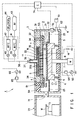
- FIG. 1 is an explanatory cross sectional view showing an etching apparatus 1 to be used for performing a plasma etching method according to an embodiment of the present invention.
- the etching apparatus 1 has a process field 2 formed in a cylindrical process chamber 3 which can be hermetically closed.
- the process chamber 3 is made of, e.g., aluminum subjected to an alumite treatment by oxidation, and is grounded through a ground line 4.
- An insulating support plate 5 made of, e.g., ceramics is disposed on the bottom of the process chamber 3.
- a susceptor 6 similar to a cylindrical column is arranged above the insulating support plate 5 for supporting thereon a target substrate W, such as a semiconductor wafer (which will be referred to as wafer).
- the susceptor 6 is movable in a vertical direction and functions as a lower electrode.
- the susceptor 6 is supported by an elevating shaft 7 penetrating the bottom of the process chamber 3 and the insulating support plate 5.
- the elevating shaft 7 is moved in a vertical direction by a driving motor 8 disposed outside the process chamber 3.
- the susceptor 6 is moved in a vertical direction by operation of the driving mortar 8, as indicated by the bidirectional arrow in FIG. 1.
- a flexible sealing member, such as bellows 9, is arranged around the elevating shaft 7 and between the susceptor 6 and the insulating support plate 5, so as to ensure the airtightness of the process chamber 3.
- the susceptor 6 is made of aluminum having an oxidized surface. Temperature adjusting means is arranged in the susceptor 6 so that the wafer 6 placed on the susceptor 6 can be kept at a predetermined temperature.
- the temperature adjusting means is formed of heating means (not shown), e.g., a ceramic heater, and a coolant circulation passage (not shown) for circulating a coolant to and from an outside coolant source (not shown).
- the temperature of the wafer W is automatically controlled by a temperature sensor (not shown) and a temperature control mechanism (not shown).
- An electrostatic chuck 11 is disposed on the susceptor 6, for attracting and holding the wafer W.
- the electrostatic chuck 11 is constituted such that a conductive thin film 12 is interposed by polyimide series resin films 13.
- a voltage of, e.g., from 1.5 kV to 2 kV is applied to the thin film 12 from a high DC power supply 14 disposed outside the process chamber 3
- the wafer W is attracted and held on the top surface of the electrostatic chuck 11 by a Coulomb's force generated at this time.
- a plurality of lifter pins 20, such as three pins, are arranged in the susceptor 6 as support means for transferring the wafer to and from the electrostatic chuck 11.
- the lifter pins 20 can lift up the wafer W from the electrostatic chuck 11 by moving in a vertical direction relative to the susceptor 6.
- An inner focus ring 21 having an essentially circular shape in its plan view is disposed on the periphery of the susceptor 6 so as to surround the electrostatic chuck 11.
- the inner focus ring 21 is made of a conductive material, such as single crystalline silicon, so as to cause plasma to expand beyond the wafer W, and to allow ions in the plasma to be effectively radiated onto the wafer W.
- An outer focus ring 22 having an essentially circular shape in its plan view is disposed around the inner focus ring 21.
- the outer focus ring 22 is made of an insulating material, such as quartz, and its outer upper edge is formed to have a curved shape projecting outward so as to allow gases to be smoothly exhausted without stagnation.
- the outer focus ring 22 cooperates with a shield ring 53 described later, so as to suppress diffusion of plasma generated between the susceptor 6 and an upper electrode 51 described later.
- the inner portion of the baffle plate 23 is fixed to the susceptor 6 by means of, e.g., bolts, through a support body made of, e.g., quartz.
- a support body made of, e.g., quartz.
- the baffle plate 23 is moved in a vertical direction along with the susceptor 6.
- a number of through holes 23a are formed in the baffle plate 23, for uniformly exhausting gases.
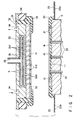
- a diffusion member 33 is arranged at the upper position of the process chamber 3 through an insulating support 31 and a cooling member 32 made of aluminum, for feeding an etching gas and other gases in the process field 2.
- a coolant circulation passage 34 is formed in the upper part of the cooling member 32. A chiller or coolant fed from the outside is circulated in the coolant circulation passage 34, so that the upper electrode 51 described later can be cooled down to a predetermined temperature.
- the diffusion member 33 has a hollow structure in which two levels of baffle plates 35 are arranged on the lower side. Each of the two levels of baffle plates 35 is provided with a number of diffusion holes 35a, such that the upper holes 35a do not overlap the lower holes 35a.
- a gas inlet 36 is formed at the center of the diffusion member 33, and is connected to a gas feed pipe 38 through a valve 37. Gas supply sources 43 and 44 are connected to the gas feed pipe 38 through respective valves 39 and 40, and respective mass flow controllers 41 and 42 for adjusting flow rates.
- An etching gas according to this embodiment i.e., HFA or HFPO
- an inactive gas such as a rare gas, e.g., argon (Ar) or helium (He), or nitrogen gas, can be fed from the gas supply source 44.
- a rare gas e.g., argon (Ar) or helium (He)
- nitrogen gas can be fed from the gas supply source 44.
- the gases from the gas supply sources 43 and 44 are introduced into the process field 2 through the gas feed pipe 38, inlet 36, and diffusion holes 35a of the diffusion member 33.
- a cooling plate 50 having a number of spouting holes 50a formed therein is disposed in close contact with the bottom surface of the cooling member 32.
- the lower electrode 51 is fixed to and in close contact with the bottom surface of the cooling plate 50, and faces the susceptor 6.
- the upper electrode 51 is made of single crystalline silicon, which is conductive, and electrically communicates with the cooling plate 50.
- the cooling plate 50 is attached to the periphery of the bottom surface of the cooling plate 50 by means of bolts (not shown).
- a number of spouting holes 51a are formed in the upper electrode 51 and communicate with the spouting holes 50a of the cooling plate 50.
- the shield ring 53 is disposed on the periphery of the bottom surface of the upper electrode 51 so as to cover the above described fixing bolts (not shown).
- the shield ring 53 is made of quartz, which is insulating, and cooperates with the outer focus ring 22 so as to form a gap narrower than that between the electrostatic chuck 11 and the upper electrode 51, thereby suppressing diffusion of plasma.
- An insulating ring 54 made of fluorine series resin is disposed between the upper end of the shield ring 53 and the ceiling wall of the process chamber 3.
- a pressure sensor 55 is attached on a side of the process chamber, for detecting the vacuum pressure of the process chamber 3.
- a detected signal of the vacuum pressure detected by the sensor 55 is inputted in a controller 74 described later, so that the vacuum pressure in the process chamber 3 is monitored all the time.
- An exhaustion pipe 62 is connected to the lower part of the process chamber 3 and communicates with vacuum exhausting means 61, such as a vacuum pump.
- the process field 2 can be vacuum-exhausted down to a predetermined vacuum pressure of, e.g., from 10 mTorr to 100 mTorr, by the vacuum exhausting means 61 through the baffle plate 23 disposed around the susceptor 6.
- the radio frequency (RF) power supply system of the etching apparatus is constituted as follows:
- the susceptor 6 used as the lower electrode is supplied with an RF power having a frequency of about several hundred kHz, such as 800 kHz, from an RF power supply 63 through a matching circuit 64.
- the upper electrode is supplied with an RF power having a frequency higher than that of the RF power supply 63 and equal to or higher than 1 MHz, such as 27.12 MHz, from an RF power supply 66 through a matching circuit 65, and the cooling member 32 and cooling plate 50.
- a load lock chamber 72 is arranged adjacent to one side of the process chamber through a gate valve 71.
- Transfer means 73 such as a transfer arm, is arranged in the load lock chamber 72, for transferring the target substrate or wafer W to and from the process field 2 in the process chamber 3.
- the driving motor 8 for moving the susceptor 6 in a vertical direction, the high DC power supply 14, the lifter pins 20 arranged in the susceptor 6, the valves 39 and 40, the mass flow controllers 41 and 42, the vacuum exhausting means 61, and the RF power supplies 63 and 66 are controlled by the controller 74.
- the gate valve 71 is opened, and the wafer W is loaded into the process chamber 3 by the transfer means 73.
- the susceptor 6 has been lowered at its lower position, and the lifter pins 20 are in a waiting state where they project from the electrostatic chuck 11 so as to receive the wafer W.
- the wafer W loaded into the process chamber 3 by the transfer means 73 is transferred onto the lifter pins 20 projecting from the electrostatic chuck 11.
- the transfer means 73 is retreated and the gate valve 71 is closed.
- the susceptor 6 is moved up to a predetermined process position where the gap between the upper electrode 51 and the susceptor 6 is set at a value of from 10 mm to 20 mm.
- the lifter pins 20 supporting the wafer W is moved down into the susceptor 6.
- the wafer W is mounted on the electrostatic chuck 11.
- a predetermined power is applied to the conductive thin film 12 of the electrostatic chuck 11 from the high DC power supply 14, so that the wafer W is attracted and held on the electrostatic chuck 11.
- the process chamber 3 is supplied with a process gas necessary for etching, which is a mixture of an etching gas and an carrier gas fed from the gas supply sources 43 and 44 at predetermined flow rates, while the process chamber 3 is vacuum-exhausted by the vacuum exhausting means 61.
- a process gas necessary for etching which is a mixture of an etching gas and an carrier gas fed from the gas supply sources 43 and 44 at predetermined flow rates
- the process chamber 3 is vacuum-exhausted by the vacuum exhausting means 61.
- the process chamber is set and kept at a predetermined vacuum pressure, such as 20 mTorr.
- the flow rate ratio between the etching gas of HFA or HFPO and the carrier gas of an inactive gas, such as Ar, i.e., the volume ratio between the etching gas and the carrier gas in the process gas, is set to fall in a range of from 1 : 10 to 1 : 30, and preferably of from 1 : 17.5 to 1 : 20. With this ratio, it is possible to obtain an excellent etching property with less deposition.
- an RF power having a frequency of 27. 12 MHz and a power of, e.g., 2 kW is applied to the upper electrode 51 from the RF power supply 66, so that the process gas is turned into plasma due to electric discharge caused between the upper electrode 51 and the susceptor 6.
- an RF power having a frequency of 800 kHz and a power of, e.g., 1 kW is applied to the susceptor 6 from the RF power supply 64.
- the process gas is dissociated in the process field so as to produce etchant ions as activated species.
- the etchant ions are further dissociated so as to produce activated species having smaller molecular weights, while they are attracted toward the susceptor 6 and controlled over their incident speeds by the RF power having a relatively low frequency and applied to the susceptor 6.
- the SiO 2 film on the wafer W is etched by means of the physical action and the chemical action of the activated species. During the etching, the target surface of the wafer is kept at a temperature of from 50°C to 100 °C.
- HFA and HFPO can present an etching rate of a silicon-oxide-based layer, such as an SiO 2 film, higher than that presented by C 4 F 8 .
- HFA and HFPO can present a sufficiently large etching selection ratio of a first layer based on silicon oxide, such as an SiO 2 film, relative to a second layer of another material, such as SiN, Si, WSi, TiSi, Al, TiN, W, photoresist or the like. Therefore, HFA and HFPO can be used for a selective etching in which the first layer is etched in preference to the second layer.
- HFA and HFPO are dissociated by electric discharge so as to produce activated species, such as C 2 F 4 , CF 3 , CF 2 , CF, and F.
- a first layer based on silicon oxide such as an SiO 2 film
- a second layer of another material containing Si such as SiN, Si, WSi, or TiSi.
- Si such as SiN, Si, WSi, or TiSi.
- their reaction with Si is promoted with an increase in content of F to decrease the etching selection ratio (the first layer/the second layer).
- C 2 F 4 exhibits a relatively high etching selection ratio, while CF 3 , F and the like exhibit low etching selection ratios. That is, in order to increase the etching selection ratio (the first layer/the second layer), the C 2 F 4 content must be increased.
- the density ratio of C 2 F 4 /CF 3 is not less than 1 in the initial stage of dissociation of HFA or HFPO, but then becomes less than 1 from a point of time when the dissociation makes progress to a certain extent. Therefore, in order to effectively use HFA or HFPO and set the density ratio of C 2 F 4 /CF 3 not to be less than 1, progress of the dissociation of HFA or HFPO should be accurately controlled.
- the density ratio of C 2 F 4 /CF 3 should be not less than 1, in a case where a first layer based on silicon oxide, such as SiO 2 film, is etched in preference to a second layer of, e.g., Al, TiN, photoresist and the like.
- Progress of the dissociation of HFA and HFPO can be controlled by adjusting their discharge duration.
- a plasma etching is performed while a process gas containing HFA or HFPO is caused to flow in a process field, the discharge duration of each part of the process gas is adjusted. With this operation, it is possible to attain an optimum etching rate and etching selection ratio for etching a silicon-oxide-based layer, such as an SiO 2 film.
- the discharge duration can be defined as a residence time of each part of the process gas in the process field 2.
- the discharge duration is defined as a sum of pulse widths within a residence time of each part of the process gas in the process chamber 3.
- the controller 74 is set based on these parameters to control the supply rate of the process gas, the exhaust rate, pulse widths of the RF power, and the like.
- HFA or HFPO is used as an etching gas for a silicon-oxide-based layer, thereby attaining a high etching rate.
- a contact hole is formed by etching, for example, an aspect ratio higher than that of a conventional method can be presented.
- the etching gas of HFA or HFPO is used with a photoresist, it is possible to provide a preferable etching property without a "sloping shoulder" of a contact hole.
- the flow rate ratio between the etching gas of HFA or HFPO and the carrier gas of an inactive gas, such as Ar, i.e., the volume ratio between the etching gas and the carrier gas in the process gas, is set to fall in a range of from 1 : 10 to 1 : 30, and preferably of from 1 : 17.5 to 1 : 20. With this ratio, it is possible to obtain an excellent etching property with less deposition.
- a contact hole was formed in an SiO 2 film by plasma etching, with a photoresist used as a mask, in each of the experiments using C 4 F 8 , and HFA and HFPO, respectively, as an etching gas.
- the flow rate ratio between the etching gas and a carrier gas of Ar was set at 1 : 17.5, the pressure in the process chamber 3 at 20 mTorr, the frequency and the power of the RF power supply 66 at 27.12 MHz and 2 kW, the frequency and the power of the RF power supply 63 at 800 kHz and 1 kW, and the temperature of the target surface of a wafer at 80°C.
- Table 1 shows etching rates (ER), etching selection ratios (SR) of the SiO 2 film to the photoresist, aspect ratios (AR), and CD losses (CDL) obtained in the experiments.
- ER etching rates
- SR etching selection ratios
- AR aspect ratios
- CDL CD losses
- HFA and HFPO presented arc etching rate and an aspect ratio higher than those presented by C 4 F 8 , and provided an excellent etching property without a "sloping shoulder".
- HFA and HFPO presented an etching selection ratio of the SiO 2 to the photoresist, nominally lower than that presented by C 4 F 8 .
- HFA and HFPO provided an excellent etching property without a "sloping shoulder”
- Table 1 ER(nm/min) SR AR CDL C 4 F 8 70-800 8-9 5-7 ⁇ HFA 1000 or more 5-6 7 or more ⁇ HFPO 900-1000 5-6 7 or more ⁇
Landscapes
- Engineering & Computer Science (AREA)
- Chemical & Material Sciences (AREA)
- Condensed Matter Physics & Semiconductors (AREA)
- Inorganic Chemistry (AREA)
- Physics & Mathematics (AREA)
- General Chemical & Material Sciences (AREA)
- Chemical Kinetics & Catalysis (AREA)
- General Physics & Mathematics (AREA)
- Manufacturing & Machinery (AREA)
- Computer Hardware Design (AREA)
- Microelectronics & Electronic Packaging (AREA)
- Power Engineering (AREA)
- Drying Of Semiconductors (AREA)
- Internal Circuitry In Semiconductor Integrated Circuit Devices (AREA)
- ing And Chemical Polishing (AREA)
Applications Claiming Priority (2)
| Application Number | Priority Date | Filing Date | Title |
|---|---|---|---|
| JP302139/95 | 1995-10-26 | ||
| JP7302139A JPH09129612A (ja) | 1995-10-26 | 1995-10-26 | エッチングガス及びエッチング方法 |
Publications (3)
| Publication Number | Publication Date |
|---|---|
| EP0776032A2 true EP0776032A2 (de) | 1997-05-28 |
| EP0776032A3 EP0776032A3 (de) | 1998-04-15 |
| EP0776032B1 EP0776032B1 (de) | 2006-03-29 |
Family
ID=17905384
Family Applications (1)
| Application Number | Title | Priority Date | Filing Date |
|---|---|---|---|
| EP96117162A Expired - Lifetime EP0776032B1 (de) | 1995-10-26 | 1996-10-25 | Plasma-Ätz-Verfahren |
Country Status (5)
| Country | Link |
|---|---|
| US (1) | US5928963A (de) |
| EP (1) | EP0776032B1 (de) |
| JP (1) | JPH09129612A (de) |
| DE (1) | DE69635972T2 (de) |
| TW (1) | TW547488U (de) |
Cited By (4)
| Publication number | Priority date | Publication date | Assignee | Title |
|---|---|---|---|---|
| EP0905757A2 (de) * | 1997-09-29 | 1999-03-31 | Siemens Aktiengesellschaft | Verbesserte Techniken für Ätzung einer Schicht auf Basis von Siliziumdioxid |
| WO1999034429A1 (en) * | 1997-12-31 | 1999-07-08 | Alliedsignal Inc. | Method of etching and cleaning using fluorinated carbonyl compounds |
| US6374833B1 (en) * | 1999-05-05 | 2002-04-23 | Mosel Vitelic, Inc. | Method of in situ reactive gas plasma treatment |
| WO2014032655A3 (de) * | 2012-08-29 | 2014-06-12 | Jacobs University Bremen Ggmbh | Halbleiterbauelement mit geschützter funktionsschicht |
Families Citing this family (36)
| Publication number | Priority date | Publication date | Assignee | Title |
|---|---|---|---|---|
| JPH1027781A (ja) * | 1996-07-10 | 1998-01-27 | Daikin Ind Ltd | エッチングガスおよびクリーニングガス |
| WO1999008805A1 (en) * | 1997-08-20 | 1999-02-25 | Air Liquide Electronics Chemicals & Services, Inc. | Plasma cleaning and etching methods using non-global-warming compounds |
| JP4602545B2 (ja) * | 1997-09-16 | 2010-12-22 | アプライド マテリアルズ インコーポレイテッド | プラズマチャンバの半導体ワークピース用シュラウド |
| US6183655B1 (en) * | 1997-09-19 | 2001-02-06 | Applied Materials, Inc. | Tunable process for selectively etching oxide using fluoropropylene and a hydrofluorocarbon |
| JP4702295B2 (ja) * | 1998-04-20 | 2011-06-15 | 株式会社日立製作所 | 半導体製造装置、および半導体検査装置 |
| JP4151749B2 (ja) * | 1998-07-16 | 2008-09-17 | 東京エレクトロンAt株式会社 | プラズマ処理装置およびその方法 |
| US6749763B1 (en) * | 1999-08-02 | 2004-06-15 | Matsushita Electric Industrial Co., Ltd. | Plasma processing method |
| US6502530B1 (en) * | 2000-04-26 | 2003-01-07 | Unaxis Balzers Aktiengesellschaft | Design of gas injection for the electrode in a capacitively coupled RF plasma reactor |
| WO2002071463A1 (en) * | 2001-03-02 | 2002-09-12 | Tokyo Electron Limited | Shower head gas injection apparatus with secondary high pressure pulsed gas injection |
| JP3527901B2 (ja) * | 2001-07-24 | 2004-05-17 | 株式会社日立製作所 | プラズマエッチング方法 |
| KR100452318B1 (ko) * | 2002-01-17 | 2004-10-12 | 삼성전자주식회사 | 압력조절시스템 및 이를 이용하는 압력조절방법 |
| US6962644B2 (en) * | 2002-03-18 | 2005-11-08 | Applied Materials, Inc. | Tandem etch chamber plasma processing system |
| US7162070B2 (en) * | 2003-06-06 | 2007-01-09 | Acushnet Company | Use of patterned, structured light to detect and measure surface defects on a golf ball |
| US20060081337A1 (en) * | 2004-03-12 | 2006-04-20 | Shinji Himori | Capacitive coupling plasma processing apparatus |
| US20080119055A1 (en) * | 2006-11-21 | 2008-05-22 | Lam Research Corporation | Reducing twisting in ultra-high aspect ratio dielectric etch |
| JP5203986B2 (ja) * | 2009-01-19 | 2013-06-05 | 東京エレクトロン株式会社 | フォーカスリングの加熱方法、プラズマエッチング方法、プラズマエッチング装置及びコンピュータ記憶媒体 |
| CN104267543B (zh) * | 2014-10-10 | 2017-07-07 | 深圳市华星光电技术有限公司 | 液晶显示面板及其制造方法 |
| US10555412B2 (en) | 2018-05-10 | 2020-02-04 | Applied Materials, Inc. | Method of controlling ion energy distribution using a pulse generator with a current-return output stage |
| US11476145B2 (en) | 2018-11-20 | 2022-10-18 | Applied Materials, Inc. | Automatic ESC bias compensation when using pulsed DC bias |
| CN118315254A (zh) | 2019-01-22 | 2024-07-09 | 应用材料公司 | 用于控制脉冲电压波形的反馈回路 |
| US11508554B2 (en) | 2019-01-24 | 2022-11-22 | Applied Materials, Inc. | High voltage filter assembly |
| US11848176B2 (en) | 2020-07-31 | 2023-12-19 | Applied Materials, Inc. | Plasma processing using pulsed-voltage and radio-frequency power |
| US11901157B2 (en) | 2020-11-16 | 2024-02-13 | Applied Materials, Inc. | Apparatus and methods for controlling ion energy distribution |
| US11798790B2 (en) | 2020-11-16 | 2023-10-24 | Applied Materials, Inc. | Apparatus and methods for controlling ion energy distribution |
| KR102582730B1 (ko) * | 2021-04-07 | 2023-09-25 | (주)후성 | 플루오르화 시클로프로판 가스의 제조방법 및 이를 포함하는 에칭용 가스 조성물 |
| US11495470B1 (en) | 2021-04-16 | 2022-11-08 | Applied Materials, Inc. | Method of enhancing etching selectivity using a pulsed plasma |
| US11791138B2 (en) | 2021-05-12 | 2023-10-17 | Applied Materials, Inc. | Automatic electrostatic chuck bias compensation during plasma processing |
| US11948780B2 (en) | 2021-05-12 | 2024-04-02 | Applied Materials, Inc. | Automatic electrostatic chuck bias compensation during plasma processing |
| US11967483B2 (en) | 2021-06-02 | 2024-04-23 | Applied Materials, Inc. | Plasma excitation with ion energy control |
| US11984306B2 (en) | 2021-06-09 | 2024-05-14 | Applied Materials, Inc. | Plasma chamber and chamber component cleaning methods |
| US11810760B2 (en) | 2021-06-16 | 2023-11-07 | Applied Materials, Inc. | Apparatus and method of ion current compensation |
| US11569066B2 (en) | 2021-06-23 | 2023-01-31 | Applied Materials, Inc. | Pulsed voltage source for plasma processing applications |
| US11776788B2 (en) | 2021-06-28 | 2023-10-03 | Applied Materials, Inc. | Pulsed voltage boost for substrate processing |
| US11476090B1 (en) | 2021-08-24 | 2022-10-18 | Applied Materials, Inc. | Voltage pulse time-domain multiplexing |
| US11694876B2 (en) | 2021-12-08 | 2023-07-04 | Applied Materials, Inc. | Apparatus and method for delivering a plurality of waveform signals during plasma processing |
| US11972924B2 (en) | 2022-06-08 | 2024-04-30 | Applied Materials, Inc. | Pulsed voltage source for plasma processing applications |
Family Cites Families (11)
| Publication number | Priority date | Publication date | Assignee | Title |
|---|---|---|---|---|
| US4260649A (en) * | 1979-05-07 | 1981-04-07 | The Perkin-Elmer Corporation | Laser induced dissociative chemical gas phase processing of workpieces |
| JPS6077429A (ja) * | 1983-10-04 | 1985-05-02 | Asahi Glass Co Ltd | ドライエツチング方法 |
| FR2619578A1 (fr) * | 1987-08-18 | 1989-02-24 | Air Liquide | Procede de gravure ionique reactive a basse tension d'autopolarisation par addition de gaz inertes |
| GB2212974B (en) * | 1987-11-25 | 1992-02-12 | Fuji Electric Co Ltd | Plasma processing apparatus |
| US5242538A (en) * | 1992-01-29 | 1993-09-07 | Applied Materials, Inc. | Reactive ion etch process including hydrogen radicals |
| JP2941572B2 (ja) * | 1992-08-11 | 1999-08-25 | 三菱電機株式会社 | プラズマエッチング装置及び半導体装置の製造方法 |
| JPH06163476A (ja) * | 1992-11-18 | 1994-06-10 | Sony Corp | ドライエッチング方法 |
| JP2957403B2 (ja) * | 1993-01-18 | 1999-10-04 | 日本電気株式会社 | プラズマエッチング方法とその装置 |
| KR960006822B1 (ko) * | 1993-04-15 | 1996-05-23 | 삼성전자주식회사 | 반도체장치의 미세패턴 형성방법 |
| JP3623256B2 (ja) * | 1993-06-30 | 2005-02-23 | 株式会社東芝 | 表面処理方法および表面処理装置 |
| US5468341A (en) * | 1993-12-28 | 1995-11-21 | Nec Corporation | Plasma-etching method and apparatus therefor |
-
1995
- 1995-10-26 JP JP7302139A patent/JPH09129612A/ja not_active Withdrawn
-
1996
- 1996-10-22 TW TW090201923U patent/TW547488U/zh not_active IP Right Cessation
- 1996-10-24 US US08/736,428 patent/US5928963A/en not_active Expired - Lifetime
- 1996-10-25 DE DE69635972T patent/DE69635972T2/de not_active Expired - Lifetime
- 1996-10-25 EP EP96117162A patent/EP0776032B1/de not_active Expired - Lifetime
Non-Patent Citations (1)
| Title |
|---|
| None |
Cited By (7)
| Publication number | Priority date | Publication date | Assignee | Title |
|---|---|---|---|---|
| EP0905757A2 (de) * | 1997-09-29 | 1999-03-31 | Siemens Aktiengesellschaft | Verbesserte Techniken für Ätzung einer Schicht auf Basis von Siliziumdioxid |
| EP0905757A3 (de) * | 1997-09-29 | 2000-10-25 | Siemens Aktiengesellschaft | Verbesserte Techniken für Ätzung einer Schicht auf Basis von Siliziumdioxid |
| WO1999034429A1 (en) * | 1997-12-31 | 1999-07-08 | Alliedsignal Inc. | Method of etching and cleaning using fluorinated carbonyl compounds |
| US6635185B2 (en) | 1997-12-31 | 2003-10-21 | Alliedsignal Inc. | Method of etching and cleaning using fluorinated carbonyl compounds |
| US6374833B1 (en) * | 1999-05-05 | 2002-04-23 | Mosel Vitelic, Inc. | Method of in situ reactive gas plasma treatment |
| WO2014032655A3 (de) * | 2012-08-29 | 2014-06-12 | Jacobs University Bremen Ggmbh | Halbleiterbauelement mit geschützter funktionsschicht |
| DE112013004302B4 (de) | 2012-08-29 | 2022-07-07 | Jacobs University Bremen Ggmbh | Elektronisches bauelement, insbesondere halbleiterbauelement, mit geschützter funktionsschicht sowie verfahren zur herstellung eines elektronischen bauelements, insbesondere eines halbleiterbauelements |
Also Published As
| Publication number | Publication date |
|---|---|
| TW547488U (en) | 2003-08-11 |
| EP0776032A3 (de) | 1998-04-15 |
| JPH09129612A (ja) | 1997-05-16 |
| EP0776032B1 (de) | 2006-03-29 |
| DE69635972D1 (de) | 2006-05-18 |
| DE69635972T2 (de) | 2006-12-07 |
| US5928963A (en) | 1999-07-27 |
Similar Documents
| Publication | Publication Date | Title |
|---|---|---|
| EP0776032B1 (de) | Plasma-Ätz-Verfahren | |
| EP0488393B1 (de) | Verfahren zur Substratbearbeitung | |
| US5997962A (en) | Plasma process utilizing an electrostatic chuck | |
| US6624082B2 (en) | Systems and methods for two-sided etch of a semiconductor substrate | |
| EP1108263B1 (de) | Erhöhter stationärer uniformitätsring | |
| US20030209324A1 (en) | Plasma reactor with reduced reaction chamber | |
| US6767698B2 (en) | High speed stripping for damaged photoresist | |
| US20140051255A1 (en) | Copper discoloration prevention following bevel etch process | |
| US20030213561A1 (en) | Atmospheric pressure plasma processing reactor | |
| US20050039854A1 (en) | Plasma etching method and plasma etching unit | |
| JP7320874B2 (ja) | 基板処理装置及び基板処理方法 | |
| JP2010161350A (ja) | 基板処理方法 | |
| JP3121524B2 (ja) | エッチング装置 | |
| EP0945896B1 (de) | Plasma-ätzmethode | |
| JPH08115901A (ja) | プラズマ処理方法およびプラズマ処理装置 | |
| US7578945B2 (en) | Method and apparatus for tuning a set of plasma processing steps | |
| JP2869384B2 (ja) | プラズマ処理方法 | |
| US4736087A (en) | Plasma stripper with multiple contact point cathode | |
| KR100323598B1 (ko) | 플라즈마에칭방법 | |
| JPH11330057A (ja) | 酸化膜のエッチング方法 | |
| EP0504758B1 (de) | Plasma-Ätzverfahren einer Silizium enthaltenden Schicht | |
| JPH09129611A (ja) | エッチング方法 | |
| KR102052337B1 (ko) | 기판 처리 장치 및 기판 처리 방법 | |
| WO2001070517A1 (en) | High speed stripping for damaged photoresist | |
| JP2003163206A (ja) | プラズマ処理装置、プラズマ処理方法及びマルチチャンバシステム |
Legal Events
| Date | Code | Title | Description |
|---|---|---|---|
| PUAI | Public reference made under article 153(3) epc to a published international application that has entered the european phase |
Free format text: ORIGINAL CODE: 0009012 |
|
| 17P | Request for examination filed |
Effective date: 19961025 |
|
| AK | Designated contracting states |
Kind code of ref document: A2 Designated state(s): DE FR GB NL |
|
| PUAL | Search report despatched |
Free format text: ORIGINAL CODE: 0009013 |
|
| AK | Designated contracting states |
Kind code of ref document: A3 Designated state(s): DE FR GB NL |
|
| 17Q | First examination report despatched |
Effective date: 20000329 |
|
| GRAP | Despatch of communication of intention to grant a patent |
Free format text: ORIGINAL CODE: EPIDOSNIGR1 |
|
| GRAS | Grant fee paid |
Free format text: ORIGINAL CODE: EPIDOSNIGR3 |
|
| GRAA | (expected) grant |
Free format text: ORIGINAL CODE: 0009210 |
|
| AK | Designated contracting states |
Kind code of ref document: B1 Designated state(s): DE FR GB NL |
|
| PG25 | Lapsed in a contracting state [announced via postgrant information from national office to epo] |
Ref country code: NL Free format text: LAPSE BECAUSE OF FAILURE TO SUBMIT A TRANSLATION OF THE DESCRIPTION OR TO PAY THE FEE WITHIN THE PRESCRIBED TIME-LIMIT Effective date: 20060329 |
|
| REG | Reference to a national code |
Ref country code: GB Ref legal event code: FG4D |
|
| REF | Corresponds to: |
Ref document number: 69635972 Country of ref document: DE Date of ref document: 20060518 Kind code of ref document: P |
|
| NLV1 | Nl: lapsed or annulled due to failure to fulfill the requirements of art. 29p and 29m of the patents act | ||
| ET | Fr: translation filed | ||
| PLBE | No opposition filed within time limit |
Free format text: ORIGINAL CODE: 0009261 |
|
| STAA | Information on the status of an ep patent application or granted ep patent |
Free format text: STATUS: NO OPPOSITION FILED WITHIN TIME LIMIT |
|
| 26N | No opposition filed |
Effective date: 20070102 |
|
| GBPC | Gb: european patent ceased through non-payment of renewal fee |
Effective date: 20061025 |
|
| PG25 | Lapsed in a contracting state [announced via postgrant information from national office to epo] |
Ref country code: GB Free format text: LAPSE BECAUSE OF NON-PAYMENT OF DUE FEES Effective date: 20061025 |
|
| PGFP | Annual fee paid to national office [announced via postgrant information from national office to epo] |
Ref country code: DE Payment date: 20141023 Year of fee payment: 19 Ref country code: FR Payment date: 20141008 Year of fee payment: 19 |
|
| REG | Reference to a national code |
Ref country code: DE Ref legal event code: R119 Ref document number: 69635972 Country of ref document: DE |
|
| PG25 | Lapsed in a contracting state [announced via postgrant information from national office to epo] |
Ref country code: DE Free format text: LAPSE BECAUSE OF NON-PAYMENT OF DUE FEES Effective date: 20160503 |
|
| REG | Reference to a national code |
Ref country code: FR Ref legal event code: ST Effective date: 20160630 |
|
| PG25 | Lapsed in a contracting state [announced via postgrant information from national office to epo] |
Ref country code: FR Free format text: LAPSE BECAUSE OF NON-PAYMENT OF DUE FEES Effective date: 20151102 |