EP0762427B1 - Semiconductor memory - Google Patents
Semiconductor memory Download PDFInfo
- Publication number
- EP0762427B1 EP0762427B1 EP96112560A EP96112560A EP0762427B1 EP 0762427 B1 EP0762427 B1 EP 0762427B1 EP 96112560 A EP96112560 A EP 96112560A EP 96112560 A EP96112560 A EP 96112560A EP 0762427 B1 EP0762427 B1 EP 0762427B1
- Authority
- EP
- European Patent Office
- Prior art keywords
- data
- inputted
- address
- outside
- processing
- Prior art date
- Legal status (The legal status is an assumption and is not a legal conclusion. Google has not performed a legal analysis and makes no representation as to the accuracy of the status listed.)
- Expired - Lifetime
Links
- 239000004065 semiconductor Substances 0.000 title claims description 10
- 238000000034 method Methods 0.000 claims description 29
- 238000006243 chemical reaction Methods 0.000 claims description 11
- 238000012905 input function Methods 0.000 claims 2
- 238000010586 diagram Methods 0.000 description 3
- 230000001360 synchronised effect Effects 0.000 description 3
- 230000003111 delayed effect Effects 0.000 description 2
- 230000000694 effects Effects 0.000 description 2
- 238000003491 array Methods 0.000 description 1
- 238000013500 data storage Methods 0.000 description 1
- 230000007423 decrease Effects 0.000 description 1
- 238000009877 rendering Methods 0.000 description 1
- 238000004904 shortening Methods 0.000 description 1
Images


Classifications
-
- G—PHYSICS
- G11—INFORMATION STORAGE
- G11C—STATIC STORES
- G11C7/00—Arrangements for writing information into, or reading information out from, a digital store
- G11C7/10—Input/output [I/O] data interface arrangements, e.g. I/O data control circuits, I/O data buffers
- G11C7/1078—Data input circuits, e.g. write amplifiers, data input buffers, data input registers, data input level conversion circuits
- G11C7/1087—Data input latches
-
- G—PHYSICS
- G11—INFORMATION STORAGE
- G11C—STATIC STORES
- G11C7/00—Arrangements for writing information into, or reading information out from, a digital store
- G11C7/10—Input/output [I/O] data interface arrangements, e.g. I/O data control circuits, I/O data buffers
- G11C7/1078—Data input circuits, e.g. write amplifiers, data input buffers, data input registers, data input level conversion circuits
- G11C7/1093—Input synchronization
-
- G—PHYSICS
- G11—INFORMATION STORAGE
- G11C—STATIC STORES
- G11C7/00—Arrangements for writing information into, or reading information out from, a digital store
- G11C7/10—Input/output [I/O] data interface arrangements, e.g. I/O data control circuits, I/O data buffers
- G11C7/1015—Read-write modes for single port memories, i.e. having either a random port or a serial port
- G11C7/1018—Serial bit line access mode, e.g. using bit line address shift registers, bit line address counters, bit line burst counters
-
- G—PHYSICS
- G11—INFORMATION STORAGE
- G11C—STATIC STORES
- G11C7/00—Arrangements for writing information into, or reading information out from, a digital store
- G11C7/10—Input/output [I/O] data interface arrangements, e.g. I/O data control circuits, I/O data buffers
- G11C7/1051—Data output circuits, e.g. read-out amplifiers, data output buffers, data output registers, data output level conversion circuits
-
- G—PHYSICS
- G11—INFORMATION STORAGE
- G11C—STATIC STORES
- G11C7/00—Arrangements for writing information into, or reading information out from, a digital store
- G11C7/10—Input/output [I/O] data interface arrangements, e.g. I/O data control circuits, I/O data buffers
- G11C7/1078—Data input circuits, e.g. write amplifiers, data input buffers, data input registers, data input level conversion circuits
-
- G—PHYSICS
- G11—INFORMATION STORAGE
- G11C—STATIC STORES
- G11C8/00—Arrangements for selecting an address in a digital store
- G11C8/18—Address timing or clocking circuits; Address control signal generation or management, e.g. for row address strobe [RAS] or column address strobe [CAS] signals
Definitions
- the present invention relates to a semiconductor memory, and particularly to a high-speed memory write method having a burst mode.
- Cache memory contains a copy of a portion of the data within the main memory. This copy of data takes as units a plurality of data units of consecutive addresses, these units being referred to as pages.
- the CPU normally accesses the cache memory. When desired data are not present within the cache memory, the desired data are newly copied from the main memory to the cache memory, this copying being carried out in page units.
- the main memory in this type of system must be capable of inputting and outputting data strings of consecutive addresses to the cache memory at high speed.
- Methods exist for this purpose in which, by merely designating the starting address, the data string including this address is inputted or outputted synchronous to a clock signal. Such a method is referred to as burst input/output, and the length of a data string which is inputted or outputted through designation of one address is known as the burst length.
- Synchronous DRAM is one typical example of memory that performs burst input/output.
- the address access time for universal DRAM is on the order of 20 ns (50 MHz).
- the time taken in processing one unit of data for synchronous DRAM is basically the same as for universal DRAM, but the apparent processing time for one unit of data can be reduced by multiplexing internal processing and processing a plurality of data units simultaneously, thereby accelerating input/output and obtaining a speed of 100 MHz.
- methods for multiplexing internal processing there exist the pipeline and prefetch methods.
- the pipeline method divides internal processing into a number of stages, and sequentially processes information relating to one unit of data through each stage (see IEICE TRANS ELECTRON., vol. E 78-C, no.7, July 1995, TOKYO, JP, pp. 782-788, Sakai et al.).
- a first unit of data processed in the first stage is processed at the second stage in the next clock cycle, while simultaneously, the second unit of data is being processed in the first stage. Because processing in each stage is carried out in parallel and simultaneously, the data of several stages is parallel processed.
- the degree of parallelism can be raised and the speed of burst input/output can be increased by increasing the number of stages and shortening the process of each stage.
- the number of points of division between stages is limited by the processing relations within the DRAM.
- the minimum clock period must agree with the stage taking the longest amount of time.
- the number of stages is actually limited to 3 or 4. In other words, the degree of data multiplexing is limited to 3 or 4.
- the prefetch method In the prefetch method, all internal processing is carried out in parallel and parallel-serial conversion is performed at the input/output section. In order to raise the degree of multiplexing in this method, the number of units of data that are parallel processed is increased. This method therefore necessitates a number of identical circuits in proportion to the degree of parallelism, thereby increasing the circuit scale and increasing the chip surface area necessary to realize the circuits. In addition, in this method the input/output of data must be performed in units of the degree of parallelism, and data in units below the degree of parallelism cannot be inputted or outputted. As a result, raising the parallelism decreases the degree of functional freedom. For these reasons, the degree of parallelism, or the degree of multiplexing, is limited to 2.
- processing of memory is carried in the order of (1) latching and processing of external signals (command, address), (2) reading of data from cell arrays, (3) output of data to the outside.
- processing proceeds in the order of (1) latching and processing of external signals (commands, address, data), and (2) writing of data to a cell array.
- data output to the outside during reading, as well as latching of data during writing involves exchange of signals with the outside and therefore precludes multiplexing at prefetching.
- input/output to a cell array can be multiplexed through prefetching by multiplexing input/output paths.
- processing and latching of commands a prefetch portion of a plurality of data units is inputted/outputted for one command, and the processing system, even a single system, can therefore perform processing for a plurality of data units.
- an internal address can be determined for a prefetch portion of a plurality of data units for one external address.
- each process may be composed of a plurality of stages.
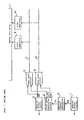
- Fig. 1 is a circuit diagram showing a prior art example
- Fig. 2 is a timing chart illustrating the operation of the prior-art example.
- the prior-art example of Fig. 1 includes a first stage from address input in which internal processing of addresses is performed and a second stage in which data input/output is performed for cells indicated by internally processed addresses. In reading, more stages are actually required for processing from this point on to data output, but these stages are here omitted because they bear no relation to this portion of the invention.
- a 2-bit prefetch operation is performed.
- Two simultaneously operating write amplifiers 9 and 10 and respectively connected data latch circuits 5 and 6 are provided for this purpose.
- Input to data latch circuits 5 and 6 is performed according to latch signals LP0 and LP1, respectively, which are outputted from latch pulse generation circuit 4'.
- latch signals LP0 and LP1 respectively, which are outputted from latch pulse generation circuit 4'.
- write command signal CMD and, from the external address terminal, the address to be written first (external address signal) EAO by burst operation, are inputted at time T0 according to standard clock signal CLK.
- External addresses are inputted only at the time of command input.
- Address buffer circuit 1 latches external address signal EA0, and based on this, internal address generation circuit 2 generates internal address signal IA0 from external address signal EA0 to bring about burst operation. A time interval of several ns is required to generate internal address signal IA0.
- Data ED0 to be written first is inputted to data-in buffer circuit 3 at the same time as external address input. This data ED0 is the starting data of the burst and is inputted to data latch circuit 5 or 6.
- the data latch circuit to which the data are inputted determines which write amplifier, 9 or 10, the data are written to, and which memory cell the data are written to. Accordingly, address signal IA0 is necessary for judging which latch signal, LP0 or LP1, to activate in order to store data to data latch circuits 5 and 6.
- internal address signal IA0 is not generated for a certain amount of time (several ns), and accordingly, data storage is delayed until the end of this time period.
- the second unit of data ED1 of the burst is inputted from the outside.
- Data ED1 undergoes the same processing as data ED0 and is stored in data latch circuit 6.
- the output of data latch circuits 5 and 6 pass through data bus 7 and 8, respectively, are formed into pairs by write amplifiers 9 and 10, and are written to memory array 11.
- a plurality of data units serially inputted from outside a chip are parallel processed within the chip, and parallel-serial conversion of data is performed to serially output to the chip exterior data that have been parallel processed within the chip.
- the external address signal and first unit of data are normally inputted from the exterior at the same time.
- the correspondence between a unit of data in a sequence and data within parallelprocessed data is determined by an address signal inputted at the same time as the first unit of data.
- the object of the present invention is to provide a semiconductor memory having a high-speed burst mode.
- a semiconductor memory and a write method according to the present invention are defined in claims 1 and 2, respectively.
- a first unit of data that is inputted according to the same standard clock as an external address and that is inputted to the chip before determination of a prefetched internal address signal is latched in all latch circuits into which this unit of data may be latched.
- the second and succeeding units of data inputted to the chip are inputted only to latch circuits that are caused to latch by address signals.
- both the first unit of data and second and succeeding units of data are latched in prefetch circuits designated by addresses from the outside.
- Fig. 1 is a circuit diagram showing an example of a semiconductor memory of the prior art.
- Fig. 2 is a timing chart for the prior-art example of Fig 1.
- Fig. 3 is a circuit diagram showing a semiconductor memory according to an embodiment of the present invention.
- Fig. 4 is a timing chart for the semiconductor memory shown in Fig. 3.
- the present embodiment includes a first stage from address input in which internal processing of addresses is performed, and a second stage in which input/output is performed with respect to cells designated by the internally processed addresses.
- a subsequent third stage is actually required for performing processing up to data output, but this stage not related to the present invention and is therefore here omitted.
- a more fractionalized pipeline configuration may also be employed.
- the second stage performs a 2-bit prefetch operation.
- Two simultaneously operating write amplifiers 9 and 10 and respectively connected data latch circuits 5 and 6 are provided for this purpose.
- Input to data latch circuits 5 and 6 is effected by latch signals LP0 and LP1, respectively, which are outputted from latch pulse generation circuit 4. While the present embodiment employs a 2-bit prefetch operation, a parallel operation involving more bits is also possible.
- write command signal CMD and the first address (external address signal) to be written in a burst operation are inputted at time T0 in accordance with standard clock signal CLK.
- External address EA is inputted only at the time of command input.
- Address buffer circuit 1 latches external address signal EA0, and based on this signal, internal address generation circuit 2 generates internal address signal IA0 from external address signal EA0 to effect the burst operation.
- the generation of IA0 requires a certain amount of time (several ns).
- data ED0 to be written first is inputted to data-in buffer circuit 3.
- This unit of data is the start data of the burst.
- These data are inputted to both data latch circuits 5 and 6 in accordance with latch signals LP0 and LP1. Accordingly, the content of both data latch circuits 5 and 6 is identical at this time. Because this operation is performed regardless of address signals, the previously mentioned generation of internal address signal IA0 from external address EA0 need not be performed.
- the second unit of data ED1 of the burst is inputted from outside at the next standard clock signal CLK.
- Data ED1 is paired with data ED0 and written to the cell array.
- generation of internal address signal IA0 has been completed, and the data latch circuit that is to latch data ED1 can therefore be determined.
- an example is shown in which data ED1 is latched in data latch circuit 5 in accordance with latch signal LP1.
Landscapes
- Engineering & Computer Science (AREA)
- Microelectronics & Electronic Packaging (AREA)
- Dram (AREA)
- Static Random-Access Memory (AREA)
Applications Claiming Priority (3)
| Application Number | Priority Date | Filing Date | Title |
|---|---|---|---|
| JP206094/95 | 1995-08-11 | ||
| JP20609495 | 1995-08-11 | ||
| JP7206094A JP2817672B2 (ja) | 1995-08-11 | 1995-08-11 | 半導体メモリ |
Publications (2)
| Publication Number | Publication Date |
|---|---|
| EP0762427A1 EP0762427A1 (en) | 1997-03-12 |
| EP0762427B1 true EP0762427B1 (en) | 2001-11-07 |
Family
ID=16517712
Family Applications (1)
| Application Number | Title | Priority Date | Filing Date |
|---|---|---|---|
| EP96112560A Expired - Lifetime EP0762427B1 (en) | 1995-08-11 | 1996-08-02 | Semiconductor memory |
Country Status (7)
| Country | Link |
|---|---|
| US (1) | US5768212A (enExample) |
| EP (1) | EP0762427B1 (enExample) |
| JP (1) | JP2817672B2 (enExample) |
| KR (1) | KR100194571B1 (enExample) |
| CN (1) | CN1106019C (enExample) |
| DE (1) | DE69616710T2 (enExample) |
| TW (1) | TW318904B (enExample) |
Families Citing this family (13)
| Publication number | Priority date | Publication date | Assignee | Title |
|---|---|---|---|---|
| US5978281A (en) * | 1999-01-04 | 1999-11-02 | International Business Machines Corporation | Method and apparatus for preventing postamble corruption within a memory system |
| US6081479A (en) * | 1999-06-15 | 2000-06-27 | Infineon Technologies North America Corp. | Hierarchical prefetch for semiconductor memories |
| US6775759B2 (en) | 2001-12-07 | 2004-08-10 | Micron Technology, Inc. | Sequential nibble burst ordering for data |
| US20040194500A1 (en) * | 2003-04-03 | 2004-10-07 | Broadway Entertainment, Inc. | Article of jewelry |
| US7652922B2 (en) * | 2005-09-30 | 2010-01-26 | Mosaid Technologies Incorporated | Multiple independent serial link memory |
| KR101293365B1 (ko) | 2005-09-30 | 2013-08-05 | 모사이드 테크놀로지스 인코퍼레이티드 | 출력 제어 메모리 |
| US20070076502A1 (en) | 2005-09-30 | 2007-04-05 | Pyeon Hong B | Daisy chain cascading devices |
| US11948629B2 (en) | 2005-09-30 | 2024-04-02 | Mosaid Technologies Incorporated | Non-volatile memory device with concurrent bank operations |
| US7688652B2 (en) * | 2007-07-18 | 2010-03-30 | Mosaid Technologies Incorporated | Storage of data in memory via packet strobing |
| US8825967B2 (en) | 2011-12-08 | 2014-09-02 | Conversant Intellectual Property Management Inc. | Independent write and read control in serially-connected devices |
| US9384851B2 (en) * | 2014-02-06 | 2016-07-05 | SK Hynix Inc. | Semiconductor devices and semiconductor systems including the same |
| JP6468763B2 (ja) * | 2014-09-08 | 2019-02-13 | ラピスセミコンダクタ株式会社 | データ処理装置 |
| CN109745693A (zh) * | 2018-12-08 | 2019-05-14 | 郑州工业应用技术学院 | 一种跳高高度自动显示装置 |
Family Cites Families (4)
| Publication number | Priority date | Publication date | Assignee | Title |
|---|---|---|---|---|
| US4775990A (en) * | 1984-01-18 | 1988-10-04 | Sharp Kabushiki Kaisha | Serial-to-parallel converter |
| JPS6139297A (ja) * | 1984-07-30 | 1986-02-25 | Nec Corp | 半導体集積回路 |
| JP2696026B2 (ja) * | 1991-11-21 | 1998-01-14 | 株式会社東芝 | 半導体記憶装置 |
| US5610864A (en) * | 1994-12-23 | 1997-03-11 | Micron Technology, Inc. | Burst EDO memory device with maximized write cycle timing |
-
1995
- 1995-08-11 JP JP7206094A patent/JP2817672B2/ja not_active Expired - Fee Related
-
1996
- 1996-07-30 US US08/688,440 patent/US5768212A/en not_active Expired - Fee Related
- 1996-08-02 DE DE69616710T patent/DE69616710T2/de not_active Expired - Fee Related
- 1996-08-02 EP EP96112560A patent/EP0762427B1/en not_active Expired - Lifetime
- 1996-08-05 TW TW085109434A patent/TW318904B/zh not_active IP Right Cessation
- 1996-08-09 CN CN96109239A patent/CN1106019C/zh not_active Expired - Fee Related
- 1996-08-10 KR KR1019960033322A patent/KR100194571B1/ko not_active Expired - Fee Related
Also Published As
| Publication number | Publication date |
|---|---|
| JP2817672B2 (ja) | 1998-10-30 |
| CN1106019C (zh) | 2003-04-16 |
| EP0762427A1 (en) | 1997-03-12 |
| JPH0955089A (ja) | 1997-02-25 |
| KR100194571B1 (ko) | 1999-06-15 |
| US5768212A (en) | 1998-06-16 |
| CN1147135A (zh) | 1997-04-09 |
| TW318904B (enExample) | 1997-11-01 |
| DE69616710T2 (de) | 2002-08-22 |
| KR970012754A (ko) | 1997-03-29 |
| DE69616710D1 (de) | 2001-12-13 |
Similar Documents
| Publication | Publication Date | Title |
|---|---|---|
| US5883855A (en) | High speed semiconductor memory with burst mode | |
| US7178001B2 (en) | Semiconductor memory asynchronous pipeline | |
| EP0762427B1 (en) | Semiconductor memory | |
| US11467965B2 (en) | Processing-in-memory (PIM) device | |
| US20010042162A1 (en) | Semiconductor memory asynchronous pipeline | |
| KR100487180B1 (ko) | 코어 잡음 테스트 실행 방법, 다이나믹 랜덤 액세스 메모리(dram) 테스트 방법, dram, 테스트 시스템, 컴퓨터 시스템 및 dram 제조 방법 | |
| JP3183159B2 (ja) | 同期型dram | |
| US6272595B1 (en) | N-way set-associative cache memory which includes a store hit buffer for improved data access | |
| JP2817685B2 (ja) | 半導体メモリ | |
| JPH07272479A (ja) | ビデオram及びそのシリアルデータ出力方法 | |
| US12106819B2 (en) | Processing-in-memory (PIM) device | |
| US11861369B2 (en) | Processing-in-memory (PIM) device | |
| JPH10134576A (ja) | 半導体メモリ装置 | |
| US12205666B2 (en) | Pipe latch circuit, operating method thereof, and semiconductor memory device including the same | |
| US11842193B2 (en) | Processing-in-memory (PIM) device | |
| US7143257B2 (en) | Method and apparatus of a smart decoding scheme for fast synchronous read in a memory system |
Legal Events
| Date | Code | Title | Description |
|---|---|---|---|
| PUAI | Public reference made under article 153(3) epc to a published international application that has entered the european phase |
Free format text: ORIGINAL CODE: 0009012 |
|
| 17P | Request for examination filed |
Effective date: 19961231 |
|
| AK | Designated contracting states |
Kind code of ref document: A1 Designated state(s): DE FR NL |
|
| 17Q | First examination report despatched |
Effective date: 19991217 |
|
| GRAG | Despatch of communication of intention to grant |
Free format text: ORIGINAL CODE: EPIDOS AGRA |
|
| GRAG | Despatch of communication of intention to grant |
Free format text: ORIGINAL CODE: EPIDOS AGRA |
|
| GRAH | Despatch of communication of intention to grant a patent |
Free format text: ORIGINAL CODE: EPIDOS IGRA |
|
| GRAH | Despatch of communication of intention to grant a patent |
Free format text: ORIGINAL CODE: EPIDOS IGRA |
|
| GRAA | (expected) grant |
Free format text: ORIGINAL CODE: 0009210 |
|
| AK | Designated contracting states |
Kind code of ref document: B1 Designated state(s): DE FR NL |
|
| REF | Corresponds to: |
Ref document number: 69616710 Country of ref document: DE Date of ref document: 20011213 |
|
| ET | Fr: translation filed | ||
| PLBE | No opposition filed within time limit |
Free format text: ORIGINAL CODE: 0009261 |
|
| STAA | Information on the status of an ep patent application or granted ep patent |
Free format text: STATUS: NO OPPOSITION FILED WITHIN TIME LIMIT |
|
| 26N | No opposition filed | ||
| NLS | Nl: assignments of ep-patents |
Owner name: NEC ELECTRONICS CORPORATION |
|
| PGFP | Annual fee paid to national office [announced via postgrant information from national office to epo] |
Ref country code: FR Payment date: 20030808 Year of fee payment: 8 |
|
| PGFP | Annual fee paid to national office [announced via postgrant information from national office to epo] |
Ref country code: DE Payment date: 20030814 Year of fee payment: 8 |
|
| PGFP | Annual fee paid to national office [announced via postgrant information from national office to epo] |
Ref country code: NL Payment date: 20030831 Year of fee payment: 8 |
|
| REG | Reference to a national code |
Ref country code: FR Ref legal event code: TP |
|
| PG25 | Lapsed in a contracting state [announced via postgrant information from national office to epo] |
Ref country code: NL Free format text: LAPSE BECAUSE OF NON-PAYMENT OF DUE FEES Effective date: 20050301 Ref country code: DE Free format text: LAPSE BECAUSE OF NON-PAYMENT OF DUE FEES Effective date: 20050301 |
|
| PG25 | Lapsed in a contracting state [announced via postgrant information from national office to epo] |
Ref country code: FR Free format text: LAPSE BECAUSE OF NON-PAYMENT OF DUE FEES Effective date: 20050429 |
|
| NLV4 | Nl: lapsed or anulled due to non-payment of the annual fee |
Effective date: 20050301 |
|
| REG | Reference to a national code |
Ref country code: FR Ref legal event code: ST |