EP0758162A2 - Gleichstromoffsetkompensationsvorrichtung - Google Patents
Gleichstromoffsetkompensationsvorrichtung Download PDFInfo
- Publication number
- EP0758162A2 EP0758162A2 EP96111445A EP96111445A EP0758162A2 EP 0758162 A2 EP0758162 A2 EP 0758162A2 EP 96111445 A EP96111445 A EP 96111445A EP 96111445 A EP96111445 A EP 96111445A EP 0758162 A2 EP0758162 A2 EP 0758162A2
- Authority
- EP
- European Patent Office
- Prior art keywords
- output
- signal
- value
- time
- time constant
- Prior art date
- Legal status (The legal status is an assumption and is not a legal conclusion. Google has not performed a legal analysis and makes no representation as to the accuracy of the status listed.)
- Granted
Links
Images


Classifications
-
- H—ELECTRICITY
- H03—ELECTRONIC CIRCUITRY
- H03F—AMPLIFIERS
- H03F1/00—Details of amplifiers with only discharge tubes, only semiconductor devices or only unspecified devices as amplifying elements
- H03F1/30—Modifications of amplifiers to reduce influence of variations of temperature or supply voltage or other physical parameters
Definitions
- This invention relates to DC offset compensation devices and more specifically to a DC offset compensation device automatically eliminating a DC offset component which is included in a received signal, a detected signal, etc., amplified by an automatic gain control function.
- a DC offset compensation device for eliminating the DC offset component of the received signal is thus installed in a receiver.
- a conventional DC offset compensation device is disclosed in Japanese Patent Laying-Open No. 62-53023, for example. The conventional DC offset compensation device is subsequently described referring to drawings.
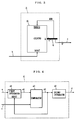
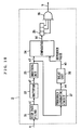
- FIG. 21 is a block diagram showing a structure of the conventional DC offset compensation device.
- the DC offset compensation device includes an adder 101, an A/D converter (ADC) 102 and a charge pump 103.
- An analog input signal ain which is band-limited and whose average of amplitude distribution is 0 is inputted to the DC offset compensation device.
- the analog input signal ain is added to a correction signal pout at the adder 101, and is converted to a digital output dout at the A/D converter 102.
- the charge pump 103 inputs a most significant bit (MSB) sgn of the digital output dout and integrates sgn to obtain the correction signal pout.
- MSB most significant bit
- the MSB sgn designates a sign of the digital output dout. That is, the MSB sgn is 0 when the digital output dout is positive, and the MSB is 1 when the digital output dout is negative. Therefore, if the digital output dout is biased to the negative side on the average, the charge pump 103 integrates 1 to gradually increase the correction signal pout. In response, the voltage level of a signal outputted by the adder 101 moves to the positive side. Therefore, the digital output dout also gradually moves to the positive side to automatically correct bias of the digital output.
- the DC offset compensation device thus outputs the digital output dout without the DC offset component.
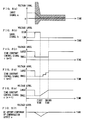
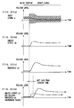
- FIGS. 22(a) to 22(d) are diagrams for describing problems when the DC offset compensation device in FIG. 21 is applied to the receiver having the AGC amplifier.
- FIG. 22(a) schematically shows a waveform of a signal inputted to the AGC amplifier.
- FIG. 22(b) shows time varying of a gain of the AGC amplifier.
- FIG. 22(c) schematically shows a waveform of a signal outputted by the AGC amplifier.
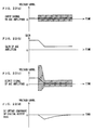
- FIG. 22(d) shows time varying in a voltage level of the DC offset component included in the digital output dout when a signal outputted by the AGC amplifier (refer to FIG. 22(c)) is inputted to the conventional DC offset compensation device.
- the input signal inputted to the AGC amplifier is a wide band signal which is band-limited and whose average of amplitude distribution is 0, as described above. Since the input signal includes a DC offset component (refer to a dash-dot line), however, the input signal is biased to the positive side. In FIG. 22 (a), only an envelope of the input signal (refer to a shaded area) is shown.
- the gain of the AGC amplifier varies a high gain to a low gain at a head portion of a received signal when the received signal rises abruptly.
- the reason for the high gain at the head portion is that the gain is controlled so as to maintain the amplitude of the signal received by the AGC amplifier in a constant voltage level.
- the AGC amplifier requires some time until it controls the gain to obtain an appropriate gain. Therefore, in the signal outputted by the AGC amplifier, its amplitude becomes extremely large at the head portion and then converges on a prescribed amplitude, as shown in FIG. 22(c).
- FIG. 22(c) shows only an envelope (refer to a shaded area) of the output signal.
- the DC offset component appearing in the signal outputted from the AGC amplifier profoundly varies according to variation of the gain. That is, as shown in FIG. 22(c), the voltage level of the DC offset component profoundly varies at the head portion (refer to a chain line). Moreover, when signals with various strength are received, the magnitude of the DC offset component appearing in the output signal of the AGC amplifier varies by signal.
- the conventional DC offset compensation device When the conventional DC offset compensation device is used in this situation, since a sufficiently large time constant is given not to distort signals, as shown in FIG. 22(d), the DC offset component profoundly varied at the head portion of the signal cannot be immediately compensated and is remained in the digital output dout for a long time.
- the time constant is set to be small so as to immediately compensate the DC offset component at the head portion of the signal, the DC offset component follows the variation of the signal itself to distort the signal.
- the amplitude is extremely large, and may be saturated or distorted. Therefore, the small time constant disturbs the operation of the DC offset compensation device and causes an erroneous operation.
- DC offset compensation devices for eliminating the DC offset component of the input signal other than the DC offset compensation device shown in FIG. 21 are disclosed in USP 5,241,702 and USP 5,212,826.
- the DC offset component extremely varied at the head portion of the input signal cannot be compensated immediately, and when the time constant is set small so as to immediately compensate the DC offset component at the head portion of the input signal, as in the case described above, the operation of the DC offset compensation device is disturbed and an erroneous operation is caused.
- An object of the present invention is to provide a DC offset compensation device capable of fast DC offset compensation at the head portion of a signal and stable DC offset compensation without distortion of the following portions of the signal when a receiver having an AGC amplifier receives a signal which immediately rises.
- the present invention is directed to a device for compensating DC offset included in an input signal, which comprises:
- the level detecting portion detects the variation in the amplitude of the input signal.
- the time constant control portion generates the time constant control signal for varying the time constant during a period corresponding to the head portion of the input signal.
- the estimating portion estimates the DC offset with the time constant varying according to the time constant control signal on the basis of the inputted compensation output. Therefore, the estimating portion can vary rapidity (time constant) for estimating the DC offset during the period corresponding to the head portion of the input signal.
- the DC offset compensation device can be thus configured capable of fast DC offset compensation at the head portion of the input signal and stable DC offset compensation at the other portions.
- the level signal is a binary signal having a first value or a second value, and a time when the level signal varies from the first value to the second value is taken as a first time, while a time lapsed for a prescribed time from the first time in a state that the level signal has the second value is taken as a second time.
- the time constant control portion outputs the time constant control signal for maximizing the time constant during a period when the level signal keeps on having the second value after the second time.
- the time constant control portion may be adapted to generate and output the time constant control signal for minimizing the time constant during a period between the first time and the second time, or the time constant control signal for monotonically increasing the time constant from the minimum to the maximum continuously or stepwise.
- the estimating portion estimates the DC offset while minimizing the time constant when the time constant control signal for minimizing the time constant is inputted.
- the DC offset compensation device can thus perform fast DC offset compensation during a period between the first time and the second time.
- the estimating portion also estimates the DC offset while varying the time constant according to variation in the time constant control signal for monotonically increasing the time constant from the minimum to the maximum continuously or stepwise.
- the DC offset compensation device can thus perform fast and precise DC offset compensation during the first time and the second time.
- the estimating portion can be configured, for example, as in the following:
- the estimating portion includes a first integrator integrating the compensation signal to output a first integration value, a comparator deciding an upper limit reference value and a lower limit reference value on the basis of the time constant control signal and comparing the first integration value with the decided upper limit reference value and lower limit reference value to output a comparison output, and a second integrator integrating the comparison output to output the estimate.
- the comparator outputs the comparison output as 0 when the first integration value is more than the lower limit reference value and less than the upper limit reference value, as +1 when the first integration value is not less than the upper limit reference value, and as -1 when the first integration value is not more than the lower limit reference value.
- the first integrator cumulatively adds the compensation outputs in the first or second structure. Furthermore, in the second structure, since the first integrator is configured by the first up/down counter, the number of its components can be decreased and the circuit configuration of the DC offset compensation device can be simplified and downsized, compared with the first structure.
- the level detecting portion detects the head portion of the input signal inputted to the DC offset compensation device from the AGC amplifier. Furthermore, in the second structure, the level detecting portion generates to output the level signal from the compensation output. DC offset is almost eliminated from this compensation output. Therefore, in the second structure, the level detecting portion does not require a high pass filter. The number of components of the level detecting portion can be decreased and the circuit configuration of the DC offset compensation device can be simplified and downsized.
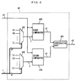
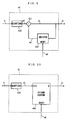
- FIG. 1 is a block diagram showing a DC offset compensation device according to a first embodiment of the present invention.
- the DC offset compensation device includes a compensator 1, a level detector 2, a time constant control circuit 3 and an estimator 4.
- the compensator 1 subtracts an estimate d inputted from the estimator 4 from an input signal a (refer to FIG. 20(a)) inputted from an AGC amplifier (not shown).
- the compensator 1 outputs the subtraction result as a compensation output e.
- the estimator 4 inputs the compensation output e to generate the estimate d. Specifically, the estimator 4 increases the estimate d when a DC offset component of the compensation output e is positive, and decreases the estimate d when the DC offset component of the compensation output e is negative.
- the counter 31 outputs a significant m bit (m ⁇ n-1) of the count value Q as a time constant control signal c from a Q terminal.
- the most significant bit (MSB) of the count value Q is inputted to an enable bar terminal (a bar is on the upper portion of ENABLE in FIG. 3 for description).
- the counter 31 stops the counting operation when the MSB of the (n-1)-th power of 2 is inputted to the enable bar terminal.
- the time constant control signal c is a binary signal.
- the time constant control signal c is a signal which controls a time for compensating the DC offset component.
- the quantizer 413 may quantize the compensation output e having a value of 0 to +1 or -1.
- the correction constant generator 404 is a selector which selects one of a plurality of predetermined positive constants according to the time constant control signal c.
- the correction constant generator 404 selects the correction constant D having a smaller value as the time constant control signal c is larger, and outputs the selected correction constant D to the adder/subtractor 403.
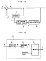
- FIG. 14 is a block diagram showing the structure of the DC offset compensation device according to a second embodiment of the present invention.
- the DC offset compensation device shown in FIG. 14 is different from the DC offset compensation device shown in FIG. 1 in that a level detector 20 is provided instead of the level detector 2. Since the other structure is the same as the structure for which the same reference numbers are provided in FIG. 1, the description is omitted.
- the level detector 20 is different from the level detector 2 shown in FIG. 1 in that the level detector 20 inputs the compensation output e to generate the level signal b according to the variation of the amplitude of the compensation output e.
- the level detector 20 may have the structure shown in FIG. 2, it may also have the following structure which is subsequently described.
- FIG. 15 is a block diagram showing the structure of the level detector 20 shown in FIG. 14.
- the level detector 20 has a structure omitting the high pass filter 21, compared with the level detector 2 shown in FIG. 2. Since the other structure is the same as the structure for which the same reference numbers are provided in FIG. 2, the description is omitted. Since the level detector 20 uses the compensation output e as an input, the DC components are almost eliminated. It is thus possible to omit the high pass filter 21.
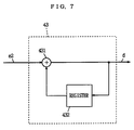
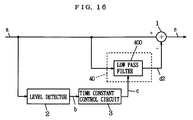
- FIG. 16 is a block diagram showing the structure of the DC offset compensation device according to a third embodiment of the present invention.
- the DC offset compensation device in FIG. 16 is different in that it has a estimator 40 instead of the estimator 4 in FIG. 1, and that the estimator 40 inputs the input signal a while the estimator 4 inputs the compensation output e in FIG. 1. Since the other structure is the same as the structure for which the same reference numbers are provided in FIG. 1, the description is omitted.
- the DC offset compensation device shown in FIG. 1 forms a feedback control loop with the estimator 4 and the compensator 1
- the DC offset compensation device shown in FIG. 16 forms a feed-forward control loop with the estimator 40 and the compensator 1.
- the DC offset device according to a fourth embodiment of the present invention is different from the structure shown in FIG. 1 in that the level detector 2 has the structure shown in FIG. 18 instead of the structure shown in FIG. 2. Therefore, the illustration of the DC offset compensation device according to the fourth embodiment is omitted. Further, since the structure other than the above described difference from that of FIG. 1 is the same as the structure for which the same reference numbers are provided in FIG. 1, the description is omitted.
- the comparator 24 shown in FIG. 2 compares the smooth output a3 with the reference value having a fixed value. Therefore, the level detector 2 shown in FIG. 2 cannot normally generate the level signal b until the smooth output a3 at the head portion of the burst-like input signal a becomes a sufficiently large value, compared with a state that the gain of the AGC amplifier converges.
- the threshold generating circuit 27 further decreases time varying of the inputted smooth output a3 to generate a threshold a4, and is typically realized by a low pass filter or an integrator.
- FIG. 19 is a block diagram showing an example of the structure of the threshold generating circuit 27 shown in FIG. 18.
- the threshold generating circuit 27 has a gain adjusting constant multiplier 271, an adder 272, a register 273 and an oblivion constant multiplier 274.
- the gain adjusting constant multiplier 271 multiplies the inputted smooth output a3 by a predetermined gain adjusting constant G to output a gain adjusting multiplier output a3'.
- the threshold a4 is obtained by multiplying the time-average of the latest components of the smooth output a3 by the gain with respect to the DC components.
- the effective average time of the threshold generating circuit 27, i.e., the time constant, is preferably several to tens of times of the symbol time of the input signal a (refer to FIG. 20(a)).
- the comparator 24 compares the smooth output a3 generated according to input of the input signal a with the delayed threshold a5 generated only on the basis of noise at the head portion of the burst-like input signal a, the level varying of the head portion of the input signal a can be precisely detected to generate the level signal b.
- the level detector 2 shown in FIG. 18 can generate the level signal b by precisely detecting the level varying at the head portion of the burst-like input signal a, compared with the level detector 2 shown in FIG. 2.
- the level detector 2 in FIG. 18 since the reference value itself varies by variation of noise and the input signal a compared with the level detector 2 shown in FIG. 2, the detection accuracy of the head portion of the burst-like signal increases, while there is a fear of generating an erroneous level signal b at the other portions.
- level detector 2 when the shift register 25 and the AND circuit 26 are omitted, i.e., the judging time is 0, the delay unit 28 can be omitted and the threshold a4 is directly taken as a reference value of the comparator 24. Further, the structure of level detector 2 can be applied to not only the level detector 2 in FIG. 1 but also the level detector in FIG. 16.
- the DC offset compensation device When the base band signal obtained by such detector is an object, if an oscillation signal of a local oscillator is leaked to be mixed into the input of the AGC amplifier to cause interference, or if an interference signal having the same frequency as that of a desired signal is simultaneously received to cause interference, the interference appears in the base band signal as the DC offset components. Therefore, in these cases, the DC offset compensation device also has the effect of reducing interference of an undesired signal.
Landscapes
- Engineering & Computer Science (AREA)
- Power Engineering (AREA)
- Control Of Amplification And Gain Control (AREA)
- Amplifiers (AREA)
- Digital Transmission Methods That Use Modulated Carrier Waves (AREA)
- Analogue/Digital Conversion (AREA)
- Dc Digital Transmission (AREA)
Applications Claiming Priority (7)
| Application Number | Priority Date | Filing Date | Title |
|---|---|---|---|
| JP202391/95 | 1995-08-08 | ||
| JP20239195 | 1995-08-08 | ||
| JP20239195 | 1995-08-08 | ||
| JP14758096A JP4091671B2 (ja) | 1995-08-08 | 1996-06-10 | 直流オフセット補償装置 |
| JP147580/96 | 1996-06-10 | ||
| JP14758096 | 1996-06-10 | ||
| US08/683,309 US5760629A (en) | 1995-08-08 | 1996-07-18 | DC offset compensation device |
Publications (3)
| Publication Number | Publication Date |
|---|---|
| EP0758162A2 true EP0758162A2 (de) | 1997-02-12 |
| EP0758162A3 EP0758162A3 (de) | 2002-07-10 |
| EP0758162B1 EP0758162B1 (de) | 2005-02-02 |
Family
ID=27319384
Family Applications (1)
| Application Number | Title | Priority Date | Filing Date |
|---|---|---|---|
| EP96111445A Expired - Lifetime EP0758162B1 (de) | 1995-08-08 | 1996-07-16 | Gleichstromoffsetkompensationsvorrichtung |
Country Status (4)
| Country | Link |
|---|---|
| US (1) | US5760629A (de) |
| EP (1) | EP0758162B1 (de) |
| JP (1) | JP4091671B2 (de) |
| CN (1) | CN1080951C (de) |
Cited By (3)
| Publication number | Priority date | Publication date | Assignee | Title |
|---|---|---|---|---|
| EP0905882A1 (de) * | 1997-09-24 | 1999-03-31 | Ando Electric Co., Ltd. | Offsetkorrektur- und Gleichstromverstärkerschaltung |
| DE102004054573A1 (de) * | 2004-11-11 | 2006-05-24 | Infineon Technologies Ag | Schaltungsanordnung und Empfangsvorrichtung |
| US7313374B2 (en) | 2003-08-01 | 2007-12-25 | Infineon Technologies Ag | Low-latency DC compensation |
Families Citing this family (54)
| Publication number | Priority date | Publication date | Assignee | Title |
|---|---|---|---|---|
| DE19637150A1 (de) * | 1996-09-12 | 1998-04-23 | Siemens Ag | Schaltung zur Ermittlung und Bewertung eines Datensignals |
| EP0895385A1 (de) * | 1997-07-29 | 1999-02-03 | Alcatel | Verminderung von Gleichstromverschiebungen für Burstbetriebempfang |
| JP3335887B2 (ja) * | 1997-08-20 | 2002-10-21 | 松下電器産業株式会社 | スペクトル拡散復調装置及びスペクトル拡散復調方法 |
| US7515896B1 (en) | 1998-10-21 | 2009-04-07 | Parkervision, Inc. | Method and system for down-converting an electromagnetic signal, and transforms for same, and aperture relationships |
| US6061551A (en) | 1998-10-21 | 2000-05-09 | Parkervision, Inc. | Method and system for down-converting electromagnetic signals |
| US7295826B1 (en) | 1998-10-21 | 2007-11-13 | Parkervision, Inc. | Integrated frequency translation and selectivity with gain control functionality, and applications thereof |
| US7236754B2 (en) | 1999-08-23 | 2007-06-26 | Parkervision, Inc. | Method and system for frequency up-conversion |
| US6560301B1 (en) | 1998-10-21 | 2003-05-06 | Parkervision, Inc. | Integrated frequency translation and selectivity with a variety of filter embodiments |
| US6813485B2 (en) | 1998-10-21 | 2004-11-02 | Parkervision, Inc. | Method and system for down-converting and up-converting an electromagnetic signal, and transforms for same |
| US6370371B1 (en) | 1998-10-21 | 2002-04-09 | Parkervision, Inc. | Applications of universal frequency translation |
| US6542722B1 (en) | 1998-10-21 | 2003-04-01 | Parkervision, Inc. | Method and system for frequency up-conversion with variety of transmitter configurations |
| US7039372B1 (en) | 1998-10-21 | 2006-05-02 | Parkervision, Inc. | Method and system for frequency up-conversion with modulation embodiments |
| US7027786B1 (en) | 1998-10-21 | 2006-04-11 | Parkervision, Inc. | Carrier and clock recovery using universal frequency translation |
| US7006805B1 (en) | 1999-01-22 | 2006-02-28 | Parker Vision, Inc. | Aliasing communication system with multi-mode and multi-band functionality and embodiments thereof, such as the family radio service |
| US7209725B1 (en) | 1999-01-22 | 2007-04-24 | Parkervision, Inc | Analog zero if FM decoder and embodiments thereof, such as the family radio service |
| US6853690B1 (en) | 1999-04-16 | 2005-02-08 | Parkervision, Inc. | Method, system and apparatus for balanced frequency up-conversion of a baseband signal and 4-phase receiver and transceiver embodiments |
| US6873836B1 (en) | 1999-03-03 | 2005-03-29 | Parkervision, Inc. | Universal platform module and methods and apparatuses relating thereto enabled by universal frequency translation technology |
| US6879817B1 (en) | 1999-04-16 | 2005-04-12 | Parkervision, Inc. | DC offset, re-radiation, and I/Q solutions using universal frequency translation technology |
| US7110435B1 (en) | 1999-03-15 | 2006-09-19 | Parkervision, Inc. | Spread spectrum applications of universal frequency translation |
| US7693230B2 (en) | 1999-04-16 | 2010-04-06 | Parkervision, Inc. | Apparatus and method of differential IQ frequency up-conversion |
| US7110444B1 (en) | 1999-08-04 | 2006-09-19 | Parkervision, Inc. | Wireless local area network (WLAN) using universal frequency translation technology including multi-phase embodiments and circuit implementations |
| US7065162B1 (en) | 1999-04-16 | 2006-06-20 | Parkervision, Inc. | Method and system for down-converting an electromagnetic signal, and transforms for same |
| US7054296B1 (en) | 1999-08-04 | 2006-05-30 | Parkervision, Inc. | Wireless local area network (WLAN) technology and applications including techniques of universal frequency translation |
| US7072390B1 (en) | 1999-08-04 | 2006-07-04 | Parkervision, Inc. | Wireless local area network (WLAN) using universal frequency translation technology including multi-phase embodiments |
| US8295406B1 (en) | 1999-08-04 | 2012-10-23 | Parkervision, Inc. | Universal platform module for a plurality of communication protocols |
| US7082171B1 (en) | 1999-11-24 | 2006-07-25 | Parkervision, Inc. | Phase shifting applications of universal frequency translation |
| US7292835B2 (en) | 2000-01-28 | 2007-11-06 | Parkervision, Inc. | Wireless and wired cable modem applications of universal frequency translation technology |
| US7010286B2 (en) | 2000-04-14 | 2006-03-07 | Parkervision, Inc. | Apparatus, system, and method for down-converting and up-converting electromagnetic signals |
| US7554508B2 (en) | 2000-06-09 | 2009-06-30 | Parker Vision, Inc. | Phased array antenna applications on universal frequency translation |
| ATE315863T1 (de) * | 2000-10-30 | 2006-02-15 | Texas Instruments Inc | Verfahren zur schätzung und entfernung eines zeitvarianten dc-offsets |
| ATE313166T1 (de) * | 2000-10-30 | 2005-12-15 | Texas Instruments Inc | Vorrichtung zum ausgleichen des dc-offsets eines quadratur-demodulators , und verfahren dazu |
| US7010559B2 (en) | 2000-11-14 | 2006-03-07 | Parkervision, Inc. | Method and apparatus for a parallel correlator and applications thereof |
| US7454453B2 (en) | 2000-11-14 | 2008-11-18 | Parkervision, Inc. | Methods, systems, and computer program products for parallel correlation and applications thereof |
| US7076225B2 (en) | 2001-02-16 | 2006-07-11 | Qualcomm Incorporated | Variable gain selection in direct conversion receiver |
| US7072427B2 (en) | 2001-11-09 | 2006-07-04 | Parkervision, Inc. | Method and apparatus for reducing DC offsets in a communication system |
| US7085335B2 (en) * | 2001-11-09 | 2006-08-01 | Parkervision, Inc. | Method and apparatus for reducing DC offsets in a communication system |
| US6975848B2 (en) * | 2002-06-04 | 2005-12-13 | Parkervision, Inc. | Method and apparatus for DC offset removal in a radio frequency communication channel |
| US7321640B2 (en) * | 2002-06-07 | 2008-01-22 | Parkervision, Inc. | Active polyphase inverter filter for quadrature signal generation |
| US8559559B2 (en) * | 2002-06-20 | 2013-10-15 | Qualcomm, Incorporated | Method and apparatus for compensating DC offsets in communication systems |
| US7379883B2 (en) | 2002-07-18 | 2008-05-27 | Parkervision, Inc. | Networking methods and systems |
| US7460584B2 (en) | 2002-07-18 | 2008-12-02 | Parkervision, Inc. | Networking methods and systems |
| EP1603228B1 (de) * | 2004-06-04 | 2010-03-10 | Infineon Technologies AG | Vorrichtung zur DC-Kompensation in einem Demodulator |
| US7519130B2 (en) * | 2005-01-18 | 2009-04-14 | International Business Machines Corporation | Front end interface for data receiver |
| US7835467B2 (en) * | 2006-01-05 | 2010-11-16 | Qualcomm, Incorporated | DC offset correction for high gain complex filter |
| JP4941894B2 (ja) * | 2007-03-30 | 2012-05-30 | 日本電気株式会社 | オフセットキャンセル回路、及びオフセットキャンセル方法 |
| JP5691186B2 (ja) * | 2010-02-10 | 2015-04-01 | アイコム株式会社 | 自動周波数制御装置および無線通信機 |
| DE102011088810B4 (de) * | 2011-12-16 | 2023-02-02 | Endress+Hauser Conducta Gmbh+Co. Kg | Elektronische Schaltung und Verfahren zum Demodulieren von Nutzsignalen aus einem Trägersignal sowie ein Modem |
| CN103441973B (zh) * | 2013-09-11 | 2017-07-28 | 陈茂奎 | 一种差分信号抑制补偿方法、装置及系统 |
| EP2869077B1 (de) * | 2013-10-30 | 2017-06-14 | Nxp B.V. | Versatzausgleich für Nulldurchgangerkennung |
| US9362894B1 (en) * | 2015-05-04 | 2016-06-07 | Freescale Semiconductor, Inc. | Clock generator circuit |
| CN104954032B (zh) * | 2015-05-22 | 2018-01-26 | 豪威科技(上海)有限公司 | 无线接收机及其使用方法 |
| JP6712071B2 (ja) * | 2016-11-14 | 2020-06-17 | 理化工業株式会社 | 波形復元装置及び波形復元方法 |
| WO2018182778A1 (en) * | 2017-03-30 | 2018-10-04 | Intel Corporation | Distributed feed-forward envelope tracking system |
| JPWO2023228663A1 (de) * | 2022-05-27 | 2023-11-30 |
Family Cites Families (9)
| Publication number | Priority date | Publication date | Assignee | Title |
|---|---|---|---|---|
| DE3312027A1 (de) * | 1983-04-02 | 1984-11-15 | Pierburg Gmbh & Co Kg, 4040 Neuss | Vorrichtung zur nullpunkteinstellung von signalquellen, insbesondere geberanordnungen |
| JP2584437B2 (ja) * | 1985-08-31 | 1997-02-26 | ソニー株式会社 | A/d変換回路 |
| US5182476A (en) * | 1991-07-29 | 1993-01-26 | Motorola, Inc. | Offset cancellation circuit and method of reducing pulse pairing |
| JP3123174B2 (ja) * | 1992-01-08 | 2001-01-09 | 株式会社豊田自動織機製作所 | センサ信号抽出回路 |
| DE4201194A1 (de) * | 1992-01-18 | 1993-07-22 | Sel Alcatel Ag | Verfahren und schaltungsanordnung zur offset-korrektur in einem tdma-funkempfaenger |
| JP2625347B2 (ja) * | 1993-04-20 | 1997-07-02 | 日本電気株式会社 | ディジタル受信器の自動オフセット制御回路 |
| EP0624000B1 (de) * | 1993-05-04 | 2000-07-19 | Koninklijke Philips Electronics N.V. | Einrichtung zur Kodierung/Dekodierung von n-bit Quellworten in entsprechende m-bit Kanalworte und umgekehrt |
| JP2669332B2 (ja) * | 1993-12-08 | 1997-10-27 | 日本電気株式会社 | 復調装置 |
| JPH0832383A (ja) * | 1994-07-14 | 1996-02-02 | Matsushita Electric Ind Co Ltd | 自動利得制御装置 |
-
1996
- 1996-06-10 JP JP14758096A patent/JP4091671B2/ja not_active Expired - Lifetime
- 1996-07-16 EP EP96111445A patent/EP0758162B1/de not_active Expired - Lifetime
- 1996-07-18 US US08/683,309 patent/US5760629A/en not_active Expired - Lifetime
- 1996-08-08 CN CN96111817A patent/CN1080951C/zh not_active Expired - Fee Related
Cited By (5)
| Publication number | Priority date | Publication date | Assignee | Title |
|---|---|---|---|---|
| EP0905882A1 (de) * | 1997-09-24 | 1999-03-31 | Ando Electric Co., Ltd. | Offsetkorrektur- und Gleichstromverstärkerschaltung |
| US6239643B1 (en) | 1997-09-24 | 2001-05-29 | Ando Electric Co., Ltd. | Offset correction circuit and DC amplification circuit |
| US7313374B2 (en) | 2003-08-01 | 2007-12-25 | Infineon Technologies Ag | Low-latency DC compensation |
| DE102004054573A1 (de) * | 2004-11-11 | 2006-05-24 | Infineon Technologies Ag | Schaltungsanordnung und Empfangsvorrichtung |
| DE102004054573B4 (de) * | 2004-11-11 | 2014-01-23 | Intel Mobile Communications GmbH | Schaltungsanordnung zum Ermitteln eines Gleichspannungs-Offset in einem Datensignal und Empfangsvorrichtung mit derselben |
Also Published As
| Publication number | Publication date |
|---|---|
| CN1145550A (zh) | 1997-03-19 |
| JP4091671B2 (ja) | 2008-05-28 |
| JPH09107254A (ja) | 1997-04-22 |
| EP0758162A3 (de) | 2002-07-10 |
| US5760629A (en) | 1998-06-02 |
| CN1080951C (zh) | 2002-03-13 |
| EP0758162B1 (de) | 2005-02-02 |
Similar Documents
| Publication | Publication Date | Title |
|---|---|---|
| EP0758162B1 (de) | Gleichstromoffsetkompensationsvorrichtung | |
| JP2909509B2 (ja) | 自動利得制御回路 | |
| US5566214A (en) | Automatic noise normalization and reacquisition control for a QPSK demodulator symbol tracking loop | |
| US5751776A (en) | Receiver for a digital communication system | |
| US7113758B2 (en) | Automatic gain controller | |
| US6173019B1 (en) | Control loop for data signal baseline correction | |
| KR100662094B1 (ko) | 고속 디지털 if agc와 아날로그 rf agc를가지는 hdtv 수신기 | |
| US6744330B1 (en) | Adaptive analog equalizer | |
| US6229469B1 (en) | Adaptive differential ADC architecture | |
| US6178201B1 (en) | Controlling an adaptive equalizer in a demodulator | |
| US7277510B1 (en) | Adaptation algorithm based on signal statistics for automatic gain control | |
| US4547888A (en) | Recursive adaptive equalizer for SMSK data links | |
| CN110995257B (zh) | 一种环路滤波电路 | |
| US5920351A (en) | Black level detecting circuit of video signal | |
| US20050123035A1 (en) | Multipath elimination filter | |
| KR100278816B1 (ko) | Dc 오프셋 보상장치 | |
| JPH11177358A (ja) | Agc回路 | |
| KR960005386B1 (ko) | 적응형 필터에 의한 자동 주파수 제어방법 및 장치 | |
| US5311314A (en) | Method of and arrangement for suppressing noise in a digital signal | |
| JPH0681162B2 (ja) | デ−タ判定回路 | |
| JP4292655B2 (ja) | サンプリング装置 | |
| KR100314921B1 (ko) | 고속데이터전송을위한위성버스트모뎀에서agc회로및그방법 | |
| JP3016738B2 (ja) | 光信号受信制御回路 | |
| KR100467528B1 (ko) | 고속 적응 이퀄라이저 | |
| JPH1141068A (ja) | ディジタル自動周波数制御回路 |
Legal Events
| Date | Code | Title | Description |
|---|---|---|---|
| PUAI | Public reference made under article 153(3) epc to a published international application that has entered the european phase |
Free format text: ORIGINAL CODE: 0009012 |
|
| AK | Designated contracting states |
Kind code of ref document: A2 Designated state(s): DE FR GB |
|
| PUAL | Search report despatched |
Free format text: ORIGINAL CODE: 0009013 |
|
| AK | Designated contracting states |
Kind code of ref document: A3 Designated state(s): DE FR GB |
|
| RIC1 | Information provided on ipc code assigned before grant |
Free format text: 7H 03F 1/30 A, 7H 03G 3/30 B |
|
| 17P | Request for examination filed |
Effective date: 20030108 |
|
| GRAP | Despatch of communication of intention to grant a patent |
Free format text: ORIGINAL CODE: EPIDOSNIGR1 |
|
| GRAS | Grant fee paid |
Free format text: ORIGINAL CODE: EPIDOSNIGR3 |
|
| GRAA | (expected) grant |
Free format text: ORIGINAL CODE: 0009210 |
|
| AK | Designated contracting states |
Kind code of ref document: B1 Designated state(s): DE FR GB |
|
| REG | Reference to a national code |
Ref country code: GB Ref legal event code: FG4D |
|
| REF | Corresponds to: |
Ref document number: 69634290 Country of ref document: DE Date of ref document: 20050310 Kind code of ref document: P |
|
| ET | Fr: translation filed | ||
| PLBE | No opposition filed within time limit |
Free format text: ORIGINAL CODE: 0009261 |
|
| STAA | Information on the status of an ep patent application or granted ep patent |
Free format text: STATUS: NO OPPOSITION FILED WITHIN TIME LIMIT |
|
| 26N | No opposition filed |
Effective date: 20051103 |
|
| REG | Reference to a national code |
Ref country code: DE Ref legal event code: R084 Ref document number: 69634290 Country of ref document: DE Effective date: 20111010 |
|
| PGFP | Annual fee paid to national office [announced via postgrant information from national office to epo] |
Ref country code: GB Payment date: 20120711 Year of fee payment: 17 |
|
| PGFP | Annual fee paid to national office [announced via postgrant information from national office to epo] |
Ref country code: FR Payment date: 20120719 Year of fee payment: 17 Ref country code: DE Payment date: 20120711 Year of fee payment: 17 |
|
| GBPC | Gb: european patent ceased through non-payment of renewal fee |
Effective date: 20130716 |
|
| REG | Reference to a national code |
Ref country code: FR Ref legal event code: ST Effective date: 20140331 |
|
| PG25 | Lapsed in a contracting state [announced via postgrant information from national office to epo] |
Ref country code: GB Free format text: LAPSE BECAUSE OF NON-PAYMENT OF DUE FEES Effective date: 20130716 Ref country code: DE Free format text: LAPSE BECAUSE OF NON-PAYMENT OF DUE FEES Effective date: 20140201 |
|
| REG | Reference to a national code |
Ref country code: DE Ref legal event code: R119 Ref document number: 69634290 Country of ref document: DE Effective date: 20140201 |
|
| PG25 | Lapsed in a contracting state [announced via postgrant information from national office to epo] |
Ref country code: FR Free format text: LAPSE BECAUSE OF NON-PAYMENT OF DUE FEES Effective date: 20130731 |