EP0751397A2 - Schaltkreis zum Setzen des Testmodus bei einem Halbleiterspeicher - Google Patents
Schaltkreis zum Setzen des Testmodus bei einem Halbleiterspeicher Download PDFInfo
- Publication number
- EP0751397A2 EP0751397A2 EP96110063A EP96110063A EP0751397A2 EP 0751397 A2 EP0751397 A2 EP 0751397A2 EP 96110063 A EP96110063 A EP 96110063A EP 96110063 A EP96110063 A EP 96110063A EP 0751397 A2 EP0751397 A2 EP 0751397A2
- Authority
- EP
- European Patent Office
- Prior art keywords
- row address
- signal
- uppermost
- test mode
- voltage
- Prior art date
- Legal status (The legal status is an assumption and is not a legal conclusion. Google has not performed a legal analysis and makes no representation as to the accuracy of the status listed.)
- Granted
Links
Images


Classifications
-
- G—PHYSICS
- G11—INFORMATION STORAGE
- G11C—STATIC STORES
- G11C29/00—Checking stores for correct operation ; Subsequent repair; Testing stores during standby or offline operation
-
- G—PHYSICS
- G11—INFORMATION STORAGE
- G11C—STATIC STORES
- G11C29/00—Checking stores for correct operation ; Subsequent repair; Testing stores during standby or offline operation
- G11C29/04—Detection or location of defective memory elements, e.g. cell constructio details, timing of test signals
- G11C29/08—Functional testing, e.g. testing during refresh, power-on self testing [POST] or distributed testing
- G11C29/12—Built-in arrangements for testing, e.g. built-in self testing [BIST] or interconnection details
- G11C29/46—Test trigger logic
-
- G—PHYSICS
- G01—MEASURING; TESTING
- G01R—MEASURING ELECTRIC VARIABLES; MEASURING MAGNETIC VARIABLES
- G01R31/00—Arrangements for testing electric properties; Arrangements for locating electric faults; Arrangements for electrical testing characterised by what is being tested not provided for elsewhere
- G01R31/28—Testing of electronic circuits, e.g. by signal tracer
- G01R31/317—Testing of digital circuits
- G01R31/3181—Functional testing
- G01R31/3185—Reconfiguring for testing, e.g. LSSD, partitioning
-
- H—ELECTRICITY
- H10—SEMICONDUCTOR DEVICES; ELECTRIC SOLID-STATE DEVICES NOT OTHERWISE PROVIDED FOR
- H10P—GENERIC PROCESSES OR APPARATUS FOR THE MANUFACTURE OR TREATMENT OF DEVICES COVERED BY CLASS H10
- H10P74/00—Testing or measuring during manufacture or treatment of wafers, substrates or devices
Definitions
- the present invention relates to a test mode setting circuit for a semiconductor device, and more particularly to a test mode setting circuit for a test circuit in a semiconductor memory in which a change to a test mode is made using a high voltage detection circuit.
- the advancement in a fine processing technology for semiconductor elements has made it possible to produce a semiconductor memory device with an increased capacity.
- the degree of integration has advanced four times in every three recent years.
- the application of such a device is increasingly expanded in fields such as information, communication, sound and image processing, and the advanced technology is contributing to the enhancement of the device performance and the miniaturization of the device as well as the decrease in power consumption.
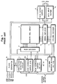
- Fig. 1 is a block diagram of the overall structure of a semiconductor memory equipped with a test mode setting circuit of the kind proposed
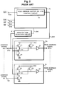
- Fig. 2 is a block diagram showing the main portion of the test mode setting circuit.
- the circuit shown comprises a clock generator 1b, lower row address buffers 2a - 2l, an uppermost row address buffer 2m, a row decoder 3, a memory cell array 4, a sense amplifier 5, a column address buffer 6, a column decoder 7, a data output buffer 8, a high voltage detection circuit 9, and a data input buffer 10.
- the clock generator 1b produces predetermined internal clock signals in response to inverted RAS (Row Address Strobe) signals, inverted CAS (Column Address Strobe) signals, inverted WE (Write Enable) signals and inverted OE (Output Enable) signals which are synchronized with clocks.
- the row address buffers 2a - 2l receive, from the outside, signals A0 - A11 among the multiplexed address signals A0 - A12, and distribute them as internal row address signals ⁇ A0 - ⁇ A11.
- the row address buffer 2m provides an internal row address signals ⁇ A12 from the signal A12, and receives a high voltage of, for example, 10 V, for the test mode setting.
- the row decoder 3 carries out decoding by using the row address signals ⁇ A0 - ⁇ A12 such that, in the case of, for example, a 64 Mbit DRAM, one of 2 13 of word lines is designated.
- the memory cell array 4 contains, for example, 64 ⁇ 10 6 memory cells designated by the row decoder.
- the sense amplifier 5 amplifies a minute voltage of data read out from the memory cell array.
- the column address buffer 6 receives the address signals A0 - A10 and distributes them as internal column address signals Y0 - Y10.
- the column decoder 7 carries out decoding by using the column address signals Y0 - Y10 such that, in the case of the 64 Mbit DRAM, one each of 2 11 of column lines is designated.
- the data output buffer 8 outputs to the outside the output data of the sense amplifier 5.
- the high voltage detection circuit 9 outputs a logical high level voltage when a voltage difference between the high voltage supplied from the outside through the common input terminal for the test mode setting and the power source voltage VCC becomes larger than a predetermined voltage.
- the data input buffer 10 supplies to the sense amplifier an external data received from the input/output terminals I/O1 - I/O4.
- the clock generator 1b has a row address control circuit 13 whose output signal is the internal clock signal ⁇ XA.
- the row address (X12) buffer 2m outputs through an in-phase buffer 21 an output of a NAND circuit.
- This NAND circuit is constituted by P-channel MOS transistors P1 and P2 having their sources connected to the power source potential line VCC and drains connected with each other with a node being formed, and N-channel MOS transistors N1 and N2 connected in series between the node and the ground.
- a drain electrode of the transistor N1 is an output node, and gate electrodes of the transistors P1 and N2 receive the address signal A12 though the input terminal In12 while gate electrodes of the transistors P2 and N1 receive the signal ⁇ XA.
- the high voltage detection circuit 9 has its input node connected to a common input terminal to which an input node of the row address buffer 2m is commonly connected, and its output node connected to an input node for the signal ⁇ sv of the clock generator 1b.
- Figs. 1 and 2 are a timing chart for use in explaining the operation of the circuit according to the invention.
- the pulse whose amplitude is about 2.0 V with the mean amplitude being about 1.5 V is supplied to the input terminals In13 - In16 which respectively receive the clock synchronisation inversion RAS signal, inversion CAS signal, inversion WE signal and inversion OE signal, to the input terminals In0 - In12 which receive the address signals A0 - A12, and to the input/output (I/O) terminal for inputting and outputting data.
- each of the clock synchronization inversion RAS signal, inversion CAS signal, and inversion OE signal is made a logical low level, thus causing the clock generator 1b to be in an active state.
- the word line of a desired memory cell in the memory cell array is selected, and the data read on the data line through the selected memory cell is amplified by the sense amplifying section 5.
- the column address (Y0-Y10) buffer 6 which distributes column addresses Y0 - Y10 and the column decoder 7, a desired sense amplifier in the sense amplifying section 5 is selected, and the output data from the selected sense amplifier is amplified at the data output buffer 8 and outputted to the external input/output terminals I/O1 - I/O4.
- the state is under a normal operation, and the output signal ⁇ sv of the high voltage detection circuit 9 is remaining as a low level, so that the test mode state is in an inactive state.
- the high voltage detection circuit 9 is arranged such that the output signal ⁇ sv thereof becomes a high level when the voltage difference between the power source voltage VCC and the voltage supplied to the input terminal In12 becomes higher than a predetermined voltage.
- the input terminal In12 is pulled-up to the high voltage and, by the inversion of the output signal ⁇ sv of the high voltage detection circuit 9 to a high level, the clock generator 1b to which the ⁇ sv is supplied turns to an active state in the test mode. That is, the input terminal In12 serves as a common terminal to which the address signal A12 or the high voltage is supplied.
- the clock generator 1b having turned to the active state is now in the test mode so that, when the internal control signal is inputted, the row decoder 3, the column address buffer 6 and the data output buffer 8 as well as the data input buffer 10 are controlled so as to carry out the operation of, for example, multi-bit simultaneous writing and reading.
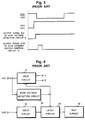
- test mode setting circuit equipped with an input circuit
- the input circuit is disclosed therein in a block diagram without showing a detailed circuit configuration.
- a circuit diagram in Fig. 4 the test mode setting circuit has an input terminal In21 which is common to an input circuit 31 and a high voltage detection circuit 33.
- the output level of the high voltage detection circuit 33 is inverted with the mode changing to a test mode, and an input circuit 31 becomes inactive.
- the test instruction data received from the input terminal In22 is supplied to a latch circuit 34 through an input circuit 32.
- This latch circuit 34 takes-in data at the inverted output level of the high voltage detection circuit 33 and, when the inverted output level restores to the original level, the data is latched and supplied to the test circuit 35, allowing the test to be carried out.
- This arrangement therefore, prevents the occurrence of such a problem that has occurred in the above explained prior art example wherein, if the high voltage is lowered for any reason during the testing, the mode changes to a non-test mode.
- the input terminal In12 which is a common terminal for supplying the address signal A12 and the high voltage is pulled-up to the high voltage and, by inverting the output signal ⁇ sv of the high voltage detection circuit 9 to a high level, the clock generator 1 to which the signal ⁇ sv is supplied is changed to an active state of the test mode.
- the P-channel MOS transistor P1 and the N-channel MOS transistors N1 and N2 that constitute a 2-input NAND circuit in the row address (X12) buffer 2m have their gate electrodes connected to the input terminal In12. Therefore, under the test mode, the high voltage supplied to the input terminal In12 is directly applied to the gate electrodes of these P-channel MOS transistor P1 and the N-channel MOS transistor N2 at the ground potential side.
- the N-channel MOS transistor N2 since the N-channel MOS transistor N2 has its source electrode connected to the ground, the voltage across the gate electrode and the source electrode and across the gate electrode and the drain electrode is in the state in which the same electric field as that of the high voltage is applied.
- Fig. 5 is a diagram showing the structure of the prior art transistor described above.
- the thin gate oxide film 47 having a thickness of about 10 nm is destroyed so that the transistor N2 having a channel 45 formed between the source electrode 44 under the gate region and the diffusion layer 46 of the drain electrode 43 no longer performs amplifying function.
- An object of the invention is to overcome the problems existing in the prior art and to provide a test mode setting circuit which is used when an internal circuit of a semiconductor integrated circuit equipped with a memory circuit is set to a test mode and in which, when a high voltage is supplied to a specified input terminal and a high voltage detection circuit inverts an output level thereof in response to the supplied voltage for the test mode setting, a gate oxide film of a first stage transistor for a specified input circuit connected to the specified input terminal is prevented from being destroyed despite the supplied high voltage.
- test mode setting circuit comprising:
- the test mode setting circuit is equipped with the voltage supplying means and includes the high voltage detection circuit, the uppermost row address buffer, and the plurality of lower row address buffers.
- the input node of the high voltage detection circuit is connected to the common input terminal of the uppermost row address buffer.
- the uppermost row address buffer receives the uppermost address signal.
- the lower row address buffers receive the lower address signals.
- the high voltage is supplied to the common input terminal and, when the upper stage one of the stacked N-channel MOS transistors which is for the particular row address buffer, among the plurality of row address buffers, for the uppermost address signal, becomes conductive by the high level voltage, the internal control signal is supplied to the lower stage one of the N-channel MOS transistors whereby this lower stage N-channel MOS transistor becomes non-conductive and, as a result, the voltage across the gate and source and the voltage across the gate and drain of the upper stage one of the N-channel MOS transistors are made lower than the high voltage. This enables the relaxing of the high electric field applied to the gate electrode and the reducing of the likelihood of the destruction of the gate oxide film.
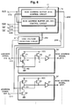
- Fig. 6 shows, in a block diagram, the main portion of the test mode setting circuit according to the invention.
- the circuit comprises a high voltage detection circuit 9, a row address (X12) buffer control circuit 11 for controlling an uppermost row address buffer X12, a row address (X0-X11) buffer control circuit 12 for controlling row address buffers X0 - X11, a clock generator 1a, a plurality of row address buffers 2a - 2l (In Fig. 6, only the row address buffer 21 is shown), and an uppermost row address buffer 2m'.
- the high voltage detection circuit 9 outputs a test mode setting signal ⁇ sv which is inverted from a low level to a high level when the voltage difference between the address signal A12 which is supplied from the outside and the power source voltage VCC becomes higher than a predetermined voltage.
- the row address buffer (X12) control circuit 11 generates an internal control clock signal ⁇ XA' upon receiving an inverted RAS signal, and makes the signal ⁇ XA' a low level when the test mode setting signal ⁇ sv supplied from the high voltage detection circuit 9 during the test mode operation becomes a high level.
- the row address (X0-X11) buffer control circuit 12 generates and outputs the internal control clock ⁇ XA both during the normal operation and the test mode operation.
- the clock generator 1a receives the inverted CAS signal, inverted WE signal and inverted OE signal, and generates respectively predetermined internal control clocks.
- the row address buffers 2a - 2l receive, from the outside, address signals A0 - A11 among the multiplexed address signals A0 - A12 and distributes them as internal row address signals ⁇ A0 - ⁇ A11.
- the uppermost row address buffer 2m' outputs through an in-phase buffer 21 the internal control clock signal ⁇ A12 generated by a logical product of the address signal A12 and the internal control clock signal ⁇ XA' and receives a high voltage VCH for the test mode setting.
- the row address (X12) buffer 2m' outputs an output of a NAND circuit through the in-phase buffer 21.
- the NAND circuit is constituted by P-channel MOS transistors (P1,P2) having source electrodes connected to a power source potential line VCC and drain electrodes interconnected thereby forming a node A, and N-channel MOS transistors (N1,N2) connected in series between the node A and a ground.
- the N-channel MOS transistor N1 has a drain electrode used as an output node, and the address signal A12 is supplied to the gate electrodes of the transistors P1 and N1, and the ⁇ XA' is supplied to the gate electrodes of the transistors P2 and N2.
- the row address buffer 21 is structurally the same as the uppermost row address buffer 2m', but the address signals A0 - A11 are supplied to the transistors P1 and N2 and the control signal ⁇ XA is supplied to the transistors P2 and N1.
- a high voltage VCH is supplied to the input terminal In12 and, when the high voltage detection circuit 9 detects that the potential difference with respect to the power source voltage VCC has exceeded a predetermined voltage, the output of the test mode setting signal ⁇ sv of the high voltage detection circuit 9 is inverted from a low level to a high level.
- the output signal ⁇ XA' of the row address buffer control circuit 11 is at the low level and this is maintained as it is.
- the signal ⁇ XA' is outputted after being inverted to the low level. Therefore, in either of these two states, the output signal ⁇ XA' becomes the low level at the point when the mode is changed to the test mode.
- the output signal ⁇ XA' having thus turned to the low level is supplied to the gate electrode of the transistor N2 at the ground potential side of the NAND circuit of the uppermost row address buffer 2m', and the transistor N2 becomes non-conductive and the transistor P2 at the ground potential side becomes conductive.
- the output node A is pulled-up to the power source potential which is of the high level and the signal ⁇ A12 is outputted through the in-phase buffer 21.
- the uppermost row address (X12) buffer 2m' in the embodiment according to the invention and the uppermost row address (X12) buffer 2m in the prior art example are the same in the point that the first stage in both the cases is constituted by the NAND circuit.
- the row address (X12) buffer control circuit 11 which corresponds to only the address signal A12 is separated from the row address (X0-X11) buffer control circuits 12 corresponding to remaining address signals A0 - A11 whereby the output signal ⁇ XA' of the row address (X12) buffer control circuit 11 is supplied to the stacked transistor N2 of the NAND circuit.
- This arrangement is different from the uppermost row address buffer 2m in the prior art example in which the output signal ⁇ XA of the row address (X0-X12) buffer control circuit 13 is supplied to the underlying transistor N1.
- the level of the signal supplied to the address signal input terminal In12 is in a range of about 2.5 V - 0.5 V which is an intermediate level when compared with the power source voltage VCC of 3 V.
- the transistor which receives the supply of the signal is the transistor N2 at the ground potential side from between the transistors N1 and N2 stacked one on the other.
- the transistor N2 can be made small in size so that this configuration is adopted in the row address (X0-X11) buffers 2a - 2l in the embodiment according to the invention.
- the output signal ⁇ XA of the row address buffer control circuit 12 is supplied to the transistor P2 and the transistor N1, and the address signals A0 - A11 are supplied to the transistors P1 and N2 as in the prior art example.
Landscapes
- Engineering & Computer Science (AREA)
- General Engineering & Computer Science (AREA)
- Physics & Mathematics (AREA)
- General Physics & Mathematics (AREA)
- For Increasing The Reliability Of Semiconductor Memories (AREA)
- Dram (AREA)
- Tests Of Electronic Circuits (AREA)
- Testing Or Measuring Of Semiconductors Or The Like (AREA)
Applications Claiming Priority (3)
| Application Number | Priority Date | Filing Date | Title |
|---|---|---|---|
| JP16625395 | 1995-06-30 | ||
| JP7166253A JPH0917196A (ja) | 1995-06-30 | 1995-06-30 | テストモード設定回路 |
| JP166253/95 | 1995-06-30 |
Publications (3)
| Publication Number | Publication Date |
|---|---|
| EP0751397A2 true EP0751397A2 (de) | 1997-01-02 |
| EP0751397A3 EP0751397A3 (de) | 1999-01-27 |
| EP0751397B1 EP0751397B1 (de) | 2001-10-17 |
Family
ID=15827961
Family Applications (1)
| Application Number | Title | Priority Date | Filing Date |
|---|---|---|---|
| EP96110063A Expired - Lifetime EP0751397B1 (de) | 1995-06-30 | 1996-06-21 | Schaltkreis zum Setzen des Testmodus bei einem Halbleiterspeicher |
Country Status (5)
| Country | Link |
|---|---|
| US (1) | US5629944A (de) |
| EP (1) | EP0751397B1 (de) |
| JP (1) | JPH0917196A (de) |
| KR (1) | KR0180449B1 (de) |
| DE (1) | DE69615940T2 (de) |
Families Citing this family (9)
| Publication number | Priority date | Publication date | Assignee | Title |
|---|---|---|---|---|
| KR100480568B1 (ko) * | 1997-10-27 | 2005-09-30 | 삼성전자주식회사 | 고전압검출부,및이를구비한반도체메모리장치와반도체메모리장치의모드구별방법 |
| US5956280A (en) * | 1998-03-02 | 1999-09-21 | Tanisys Technology, Inc. | Contact test method and system for memory testers |
| KR100286101B1 (ko) * | 1999-04-17 | 2001-03-15 | 윤종용 | 반도체 장치의 신호 발생회로 |
| JP2003016800A (ja) * | 2001-07-03 | 2003-01-17 | Mitsubishi Electric Corp | 半導体装置 |
| JP3943890B2 (ja) * | 2001-10-18 | 2007-07-11 | 富士通株式会社 | 半導体装置 |
| US7298656B2 (en) * | 2004-04-30 | 2007-11-20 | Infineon Technologies Ag | Process monitoring by comparing delays proportional to test voltages and reference voltages |
| KR100851550B1 (ko) * | 2007-02-27 | 2008-08-11 | 삼성전자주식회사 | 테스트 시스템 및 그것의 고전압 측정 방법 |
| JP2018032981A (ja) * | 2016-08-24 | 2018-03-01 | 株式会社東芝 | 半導体集積回路 |
| CN113325292B (zh) * | 2021-07-09 | 2022-11-22 | 华北电力大学 | 功率半导体器件栅氧性能参数测量电路及其测量方法 |
Family Cites Families (8)
| Publication number | Priority date | Publication date | Assignee | Title |
|---|---|---|---|---|
| US5051995A (en) * | 1988-03-14 | 1991-09-24 | Mitsubishi Denki Kabushiki Kaisha | Semiconductor memory device having a test mode setting circuit |
| JPH02213779A (ja) * | 1989-02-15 | 1990-08-24 | Hitachi Ltd | 半導体集積回路装置 |
| JPH0314238A (ja) * | 1989-06-13 | 1991-01-22 | Oki Electric Ind Co Ltd | バイポーラ型半導体集積回路装置の製造方法 |
| US5155704A (en) * | 1990-10-16 | 1992-10-13 | Micron Technology, Inc. | Memory integrated circuit test mode switching |
| KR960002006B1 (ko) * | 1991-03-12 | 1996-02-09 | 가부시끼가이샤 도시바 | 2개의 기준 레벨을 사용하는 기록 검증 제어기를 갖는 전기적으로 소거 가능하고 프로그램 가능한 불휘발성 메모리 장치 |
| JP2894068B2 (ja) * | 1992-01-30 | 1999-05-24 | 日本電気株式会社 | 半導体集積回路 |
| JPH0757484A (ja) * | 1993-08-11 | 1995-03-03 | Sony Corp | Nor型不揮発性メモリ制御回路 |
| US5544175A (en) * | 1994-03-15 | 1996-08-06 | Hewlett-Packard Company | Method and apparatus for the capturing and characterization of high-speed digital information |
-
1995
- 1995-06-30 JP JP7166253A patent/JPH0917196A/ja active Pending
-
1996
- 1996-06-21 EP EP96110063A patent/EP0751397B1/de not_active Expired - Lifetime
- 1996-06-21 DE DE69615940T patent/DE69615940T2/de not_active Expired - Fee Related
- 1996-06-25 US US08/670,823 patent/US5629944A/en not_active Expired - Fee Related
- 1996-06-29 KR KR1019960026061A patent/KR0180449B1/ko not_active Expired - Fee Related
Also Published As
| Publication number | Publication date |
|---|---|
| JPH0917196A (ja) | 1997-01-17 |
| KR970002371A (ko) | 1997-01-24 |
| EP0751397A3 (de) | 1999-01-27 |
| US5629944A (en) | 1997-05-13 |
| KR0180449B1 (ko) | 1999-04-01 |
| EP0751397B1 (de) | 2001-10-17 |
| DE69615940T2 (de) | 2002-04-25 |
| DE69615940D1 (de) | 2001-11-22 |
Similar Documents
| Publication | Publication Date | Title |
|---|---|---|
| US5051995A (en) | Semiconductor memory device having a test mode setting circuit | |
| KR100245943B1 (ko) | 고속 데이타 입/출력이 가능한 소 점유면적의 데이타 입/출력 회로를 구비한 반도체 메모리 장치 | |
| US11087805B2 (en) | Apparatus with a biasing mechanism and methods for operating the same | |
| US5640363A (en) | Semiconductor memory device | |
| US5917765A (en) | Semiconductor memory device capable of burn in mode operation | |
| EP0920032B1 (de) | Ferroelektrischer Direktzugriffspeicher mit kurzlebigem Zelldetektor für Prüfung eines ferroelektrischen Kapazitors und Verfahren zur Prüfung von ferroelekrischen Speicherzellen | |
| US7113435B2 (en) | Data compression read mode for memory testing | |
| US5475646A (en) | Screening circuitry for a dynamic random access memory | |
| US6154864A (en) | Read only memory embedded in a dynamic random access memory | |
| US6649984B1 (en) | Logic-merged memory | |
| US6823485B1 (en) | Semiconductor storage device and test system | |
| US5629944A (en) | Test mode setting circuit of test circuit for semiconductor memory | |
| KR100301645B1 (ko) | 테스트모드에있어서워드선을임의로또한고속으로선택상태로하는선택회로를갖는반도체기억장치 | |
| KR20010086356A (ko) | 반도체 메모리 | |
| EP0456254A2 (de) | Halbleiteranordnung und ihre Prüfungsverfahren | |
| US5774472A (en) | Semiconductor memory device capable of realizing stable test mode operation | |
| US6222781B1 (en) | Semiconductor integrated circuit device capable of externally applying power supply potential to internal circuit while restricting noise | |
| US6804154B2 (en) | Semiconductor memory device including power generation circuit implementing stable operation | |
| JP2004071119A (ja) | 半導体記憶装置 | |
| KR100302424B1 (ko) | 논리하이브리드메모리용반도체메모리 | |
| US6496433B2 (en) | Semiconductor device and semiconductor device testing method | |
| US6597040B2 (en) | Semiconductor device having MOS transistor for coupling two signal lines | |
| US20040233764A1 (en) | Semiconductor memory device having self-precharge function | |
| JP2003168300A (ja) | 半導体装置 | |
| US6567336B2 (en) | Semiconductor memory for logic-hybrid memory |
Legal Events
| Date | Code | Title | Description |
|---|---|---|---|
| PUAI | Public reference made under article 153(3) epc to a published international application that has entered the european phase |
Free format text: ORIGINAL CODE: 0009012 |
|
| AK | Designated contracting states |
Kind code of ref document: A2 Designated state(s): DE FR GB |
|
| PUAL | Search report despatched |
Free format text: ORIGINAL CODE: 0009013 |
|
| RHK1 | Main classification (correction) |
Ipc: G11C 29/00 |
|
| AK | Designated contracting states |
Kind code of ref document: A3 Designated state(s): DE FR GB |
|
| 17P | Request for examination filed |
Effective date: 19990301 |
|
| 17Q | First examination report despatched |
Effective date: 20000301 |
|
| GRAG | Despatch of communication of intention to grant |
Free format text: ORIGINAL CODE: EPIDOS AGRA |
|
| GRAG | Despatch of communication of intention to grant |
Free format text: ORIGINAL CODE: EPIDOS AGRA |
|
| GRAH | Despatch of communication of intention to grant a patent |
Free format text: ORIGINAL CODE: EPIDOS IGRA |
|
| GRAH | Despatch of communication of intention to grant a patent |
Free format text: ORIGINAL CODE: EPIDOS IGRA |
|
| GRAA | (expected) grant |
Free format text: ORIGINAL CODE: 0009210 |
|
| AK | Designated contracting states |
Kind code of ref document: B1 Designated state(s): DE FR GB |
|
| REF | Corresponds to: |
Ref document number: 69615940 Country of ref document: DE Date of ref document: 20011122 |
|
| REG | Reference to a national code |
Ref country code: GB Ref legal event code: IF02 |
|
| ET | Fr: translation filed | ||
| PGFP | Annual fee paid to national office [announced via postgrant information from national office to epo] |
Ref country code: FR Payment date: 20020610 Year of fee payment: 7 |
|
| PGFP | Annual fee paid to national office [announced via postgrant information from national office to epo] |
Ref country code: GB Payment date: 20020619 Year of fee payment: 7 |
|
| PGFP | Annual fee paid to national office [announced via postgrant information from national office to epo] |
Ref country code: DE Payment date: 20020626 Year of fee payment: 7 |
|
| PLBE | No opposition filed within time limit |
Free format text: ORIGINAL CODE: 0009261 |
|
| STAA | Information on the status of an ep patent application or granted ep patent |
Free format text: STATUS: NO OPPOSITION FILED WITHIN TIME LIMIT |
|
| 26N | No opposition filed | ||
| PG25 | Lapsed in a contracting state [announced via postgrant information from national office to epo] |
Ref country code: GB Free format text: LAPSE BECAUSE OF NON-PAYMENT OF DUE FEES Effective date: 20030621 |
|
| PG25 | Lapsed in a contracting state [announced via postgrant information from national office to epo] |
Ref country code: DE Free format text: LAPSE BECAUSE OF NON-PAYMENT OF DUE FEES Effective date: 20040101 |
|
| GBPC | Gb: european patent ceased through non-payment of renewal fee |
Effective date: 20030621 |
|
| PG25 | Lapsed in a contracting state [announced via postgrant information from national office to epo] |
Ref country code: FR Free format text: LAPSE BECAUSE OF NON-PAYMENT OF DUE FEES Effective date: 20040227 |
|
| REG | Reference to a national code |
Ref country code: FR Ref legal event code: ST |