EP0740348B1 - Halbleiter-Speichervorrichtung unter Verwendung eines ferroelektrischen Dielektrikums und Verfahren zur Herstellung - Google Patents
Halbleiter-Speichervorrichtung unter Verwendung eines ferroelektrischen Dielektrikums und Verfahren zur Herstellung Download PDFInfo
- Publication number
- EP0740348B1 EP0740348B1 EP95106101A EP95106101A EP0740348B1 EP 0740348 B1 EP0740348 B1 EP 0740348B1 EP 95106101 A EP95106101 A EP 95106101A EP 95106101 A EP95106101 A EP 95106101A EP 0740348 B1 EP0740348 B1 EP 0740348B1
- Authority
- EP
- European Patent Office
- Prior art keywords
- capacitor
- layer
- trench
- semiconductor memory
- dielectric
- Prior art date
- Legal status (The legal status is an assumption and is not a legal conclusion. Google has not performed a legal analysis and makes no representation as to the accuracy of the status listed.)
- Expired - Lifetime
Links
- 239000004065 semiconductor Substances 0.000 title claims abstract description 59
- 238000000034 method Methods 0.000 title claims abstract description 38
- 230000015572 biosynthetic process Effects 0.000 title description 5
- 239000003990 capacitor Substances 0.000 claims abstract description 107
- 239000000758 substrate Substances 0.000 claims abstract description 23
- 238000000151 deposition Methods 0.000 claims abstract description 20
- 238000003860 storage Methods 0.000 claims description 33
- 238000001465 metallisation Methods 0.000 claims description 17
- BASFCYQUMIYNBI-UHFFFAOYSA-N platinum Chemical compound [Pt] BASFCYQUMIYNBI-UHFFFAOYSA-N 0.000 claims description 17
- 239000000463 material Substances 0.000 claims description 14
- 229910052697 platinum Inorganic materials 0.000 claims description 9
- 239000010936 titanium Substances 0.000 claims description 9
- 125000006850 spacer group Chemical group 0.000 claims description 8
- 229910052719 titanium Inorganic materials 0.000 claims description 8
- RTAQQCXQSZGOHL-UHFFFAOYSA-N Titanium Chemical compound [Ti] RTAQQCXQSZGOHL-UHFFFAOYSA-N 0.000 claims description 7
- 230000015654 memory Effects 0.000 claims description 7
- WFKWXMTUELFFGS-UHFFFAOYSA-N tungsten Chemical compound [W] WFKWXMTUELFFGS-UHFFFAOYSA-N 0.000 claims description 7
- 229910052721 tungsten Inorganic materials 0.000 claims description 7
- 239000010937 tungsten Substances 0.000 claims description 7
- 238000005530 etching Methods 0.000 claims description 6
- 239000004020 conductor Substances 0.000 claims description 5
- 229910052751 metal Inorganic materials 0.000 claims description 5
- 239000002184 metal Substances 0.000 claims description 5
- NRTOMJZYCJJWKI-UHFFFAOYSA-N Titanium nitride Chemical compound [Ti]#N NRTOMJZYCJJWKI-UHFFFAOYSA-N 0.000 claims description 4
- HFGPZNIAWCZYJU-UHFFFAOYSA-N lead zirconate titanate Chemical compound [O-2].[O-2].[O-2].[O-2].[O-2].[Ti+4].[Zr+4].[Pb+2] HFGPZNIAWCZYJU-UHFFFAOYSA-N 0.000 claims description 4
- 239000005380 borophosphosilicate glass Substances 0.000 claims description 3
- -1 strontium tantalate compound Chemical class 0.000 claims description 3
- 239000011521 glass Substances 0.000 claims description 2
- VYPSYNLAJGMNEJ-UHFFFAOYSA-N Silicium dioxide Chemical compound O=[Si]=O VYPSYNLAJGMNEJ-UHFFFAOYSA-N 0.000 claims 2
- 229910052681 coesite Inorganic materials 0.000 claims 1
- 229910052906 cristobalite Inorganic materials 0.000 claims 1
- 239000000377 silicon dioxide Substances 0.000 claims 1
- 238000009987 spinning Methods 0.000 claims 1
- 229910052682 stishovite Inorganic materials 0.000 claims 1
- 229910052905 tridymite Inorganic materials 0.000 claims 1
- 150000003658 tungsten compounds Chemical class 0.000 claims 1
- 238000004519 manufacturing process Methods 0.000 abstract description 17
- 208000023414 familial retinal arterial macroaneurysm Diseases 0.000 description 12
- 230000008021 deposition Effects 0.000 description 5
- 238000005516 engineering process Methods 0.000 description 5
- 239000000126 substance Substances 0.000 description 5
- 229910004298 SiO 2 Inorganic materials 0.000 description 4
- 230000010354 integration Effects 0.000 description 4
- 238000004528 spin coating Methods 0.000 description 4
- 238000010438 heat treatment Methods 0.000 description 3
- 229910021420 polycrystalline silicon Inorganic materials 0.000 description 3
- KRHYYFGTRYWZRS-UHFFFAOYSA-N Fluorane Chemical compound F KRHYYFGTRYWZRS-UHFFFAOYSA-N 0.000 description 2
- ATJFFYVFTNAWJD-UHFFFAOYSA-N Tin Chemical compound [Sn] ATJFFYVFTNAWJD-UHFFFAOYSA-N 0.000 description 2
- 238000010586 diagram Methods 0.000 description 2
- 239000003989 dielectric material Substances 0.000 description 2
- 239000000945 filler Substances 0.000 description 2
- 238000006243 chemical reaction Methods 0.000 description 1
- 239000011365 complex material Substances 0.000 description 1
- 150000001875 compounds Chemical class 0.000 description 1
- 239000013078 crystal Substances 0.000 description 1
- 238000002425 crystallisation Methods 0.000 description 1
- 230000008025 crystallization Effects 0.000 description 1
- 238000005137 deposition process Methods 0.000 description 1
- IVUXZQJWTQMSQN-UHFFFAOYSA-N distrontium;oxygen(2-);tantalum(5+) Chemical compound [O-2].[O-2].[O-2].[O-2].[O-2].[O-2].[O-2].[Sr+2].[Sr+2].[Ta+5].[Ta+5] IVUXZQJWTQMSQN-UHFFFAOYSA-N 0.000 description 1
- 238000005265 energy consumption Methods 0.000 description 1
- 230000035876 healing Effects 0.000 description 1
- 229910052739 hydrogen Inorganic materials 0.000 description 1
- 239000001257 hydrogen Substances 0.000 description 1
- 125000004435 hydrogen atom Chemical class [H]* 0.000 description 1
- 238000002161 passivation Methods 0.000 description 1
- 238000001020 plasma etching Methods 0.000 description 1
- 239000007787 solid Substances 0.000 description 1
- 239000002904 solvent Substances 0.000 description 1
- 239000010409 thin film Substances 0.000 description 1
- 238000003631 wet chemical etching Methods 0.000 description 1
Images

Classifications
-
- H—ELECTRICITY
- H10—SEMICONDUCTOR DEVICES; ELECTRIC SOLID-STATE DEVICES NOT OTHERWISE PROVIDED FOR
- H10B—ELECTRONIC MEMORY DEVICES
- H10B12/00—Dynamic random access memory [DRAM] devices
-
- H—ELECTRICITY
- H10—SEMICONDUCTOR DEVICES; ELECTRIC SOLID-STATE DEVICES NOT OTHERWISE PROVIDED FOR
- H10B—ELECTRONIC MEMORY DEVICES
- H10B12/00—Dynamic random access memory [DRAM] devices
- H10B12/01—Manufacture or treatment
- H10B12/02—Manufacture or treatment for one transistor one-capacitor [1T-1C] memory cells
- H10B12/03—Making the capacitor or connections thereto
- H10B12/033—Making the capacitor or connections thereto the capacitor extending over the transistor
-
- H—ELECTRICITY
- H10—SEMICONDUCTOR DEVICES; ELECTRIC SOLID-STATE DEVICES NOT OTHERWISE PROVIDED FOR
- H10B—ELECTRONIC MEMORY DEVICES
- H10B53/00—Ferroelectric RAM [FeRAM] devices comprising ferroelectric memory capacitors
Definitions
- the invention relates to a method of manufacture a capacitor and a semiconductor memory device with a plurality of arranged on a semiconductor substrate Memory cells, each one in one Arranged semiconductor substrate and each have a gate connection and a first and a second electrode connection having a selection transistor and a selection transistor assigned and controllable by this Storage capacitor with a ferroelectric dielectric and a first and a second capacitor electrode has, each gate terminal of the selection transistor with a word line of the semiconductor memory device, each first electrode connection of the selection transistor with a Bit line, and each first capacitor electrode of the storage capacitor with a common conductor layer made of electrical conductive material is connected, as well as a process for manufacturing such a semiconductor memory device.
- Such a semiconductor memory device with a storage capacitor with a ferroelectric dielectric is known, for example, from R. Moazzami et al, Symposium on VLSI Technology Digest of Technical Papers 1994, pages 55 ff., And Tatsumi Sumi et al., IEEE International Solid -State Circuits Conference 1994, pages 268 ff., In which semiconductor memory device the storage capacitors with the ferroelectric dielectric are planar and also have considerable cell areas per bit due to the wiring, which is considered disadvantageous in view of a desired high integration density. Despite the problems that still exist, ferroelectric memories or FRAMs are predicted to have a great future.
- DRAM semiconductor memories with conventional materials for the dielectric of the storage capacitor known.
- DRAM semiconductor memory with a storage capacity from currently to about 256 megabytes of dielectric with one high dielectric constant used to at low sufficient cell area, typically of more than about 20 fF per cell.
- a ONO layer used in which meanwhile the technological Limits are recognizable because the leakage current is above the specified one Limit for a further reduction in thickness increases, and sufficient capacities (areas) only using complex structures such as trench or stacked capacitors can be obtained.
- EP-A-0 503 078 is a FRAM semiconductor memory cell with a planar storage capacitor with ferroelectric Dielectric, lower capacitor electrode, as well known upper capacitor electrode.
- DE-A-3 922 456 is a conventional DRAM semiconductor memory device with a layered capacitor cell known.
- the invention is based on this prior art the task of a method for producing a Capacitor and a semiconductor memory device with specify a storage capacitor, which is one of the previous Semiconductor memory device approximately comparable Integration density with correspondingly high reliability and Has quality and with comparatively little effort in existing process flows can be integrated, suitable for series production is, i.e. a high yield of finished Semiconductor memory devices with a storage capacitor enables the lowest possible number of early failures.
- This object is achieved by a method for Production of a capacitor according to claim 1 and by a semiconductor memory device according to claim 8 solved.
- the step of depositing the dielectric Layer carried out by spin coating.
- dielectric layers in a layer thickness in the nanometer range are applied, preferred because of their viscous, lacquer-like consistency can be applied in a spin process.
- the dielectric is spun on, whereby the Material of the dielectric preferably as in a solvent introduced substance is present in the exposed Hollow layer between the two electrically conductive Layers deposited for the first and second capacitor electrodes.
- Dielectric is a ferroelectric gel, which by Spin coating is applied.
- the dielectric another, not necessarily ferroelectric Represent substance by the spin process is to be applied, in particular such a substance for the dielectric with a compared to the previously known substances larger dielectric constant.
- the invention is also a semiconductor memory device of the generic type provided in which the Selection transistor associated storage capacitor with the ferroelectric dielectric versus the plane of the Has substrate surface upstanding arrangement.
- This design of the storage capacitor with the ferroelectric dielectric in a towering The arrangement enables the smallest possible area the FRAM cell still has a sufficient capacity of the storage capacitor to achieve, the invention Formation with a plane opposite the substrate surface towering arrangement of the ferroelectric storage capacitor the training of the desired high Integration density of critical ferroelectric materials after a complete production of less in this regard critical components of the memory cell, i.e. select transistors with full metallization including associated electrodes, preferably in that the to be applied by means of centrifugal technology ferroelectric gel within one between the two capacitor electrodes trained thin hollow layer introduced is, with the hollow layer also opposite has an upstanding arrangement on the plane of the substrate surface.
- the opposite arrangement upstanding on the plane of the substrate surface of the storage capacitor with the ferroelectric dielectric is essentially cylindrical symmetrical with one at least approximately perpendicular to the plane of the substrate surface extending cylinder center axis.
- the second capacitor electrode inside the trench trained storage capacitor can be compliant to the vertical side walls of the trench of deposited metal spacers be trained.
- first capacitor electrode of the storage capacitor one formed within the trench, coaxial to the longitudinal extent of the trench and opposite the second capacitor electrode extending electrode section, and the ferroelectric dielectric at least between the Electrode section of the first capacitor electrode and the second capacitor electrode is arranged.
- the first capacitor electrode of the storage capacitor cup-shaped formed within the second capacitor electrode his.
- the method according to the invention provides for the selection transistor assigned storage capacitor with the ferroelectric Dielectric after completion of the selection transistor and its associated metallization layers for connecting the word and bit lines in one opposite the plane of the surface of the semiconductor substrate in the towering parallel arranged selection transistor Manufacturing arrangement.
- the storage capacitor with the ferroelectric dielectric in one inside the already existing contact metallization layer for the second electrode connection of the selection transistor trained trench, the depth of the trench corresponds to the layer thickness of the contact metallization layer.
- the concept of the method according to the invention lies here First, the knowledge is based on a semiconductor memory device or a process flow for manufacturing the semiconductor memory device specify where the ferroelectric Materials in the process flow for making the Semiconductor memory device can be successfully integrated can, namely in that only after the manufacture of fully formed selection transistors including complete Metallization including all of the selection transistor assigned electrodes applied the dielectric material and to carry out the necessary crystallization is subjected to a heat treatment.
- the method according to the invention enables the production of a FRAM memory device, whose space requirement is just as small is like a RAM cell, by means of one Process step sequence that can be integrated into existing process flows.
- the layer thickness of the ferroelectric dielectric can preferably set precisely in the nanometer range become.
- the step of separating the dielectric having ferroelectric dielectric Layer carried out by spin coating.
- the method according to the invention is characterized by the following further method steps: Etching back the electrically conductive layer for the second capacitor electrode, which is deposited conformally to the inner contour of the trench, at least to the extent that the part of the electrically conductive layer for the second capacitor electrode which is planarly deposited outside the trench is removed. In this way, the risk of an electrical short circuit of the two capacitor electrodes is reduced.
- the ferroelectric dielectric is a ferroelectric Gel, which in particular is a lead zirconium titanate (PZT) and / or a strontium tantalate compound having.
- PZT lead zirconium titanate
- the material of the layer for the first one and / or second capacitor electrode, preferably titanium and / or platinum, the layer for the first and / or second capacitor electrode also formed as a multilayer can be, preferably with a layer sequence Titanium / titanium nitride / platinum or titanium / titanium nitride / tungsten.
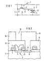
- a semiconductor memory device with an FRAM cell 1 according to the equivalent circuit diagram according to FIG. 1 has a selection transistor 3 formed on a semiconductor substrate 2, preferably of the MOS type, with a first electrode connection 5 connected to a bit line 4 made of tungsten or polycide ( Source), a second electrode connection 6 (drain) and a gate connection 8 connected to a word line 7 made of n + -Poly-Si or polyzide, and a storage capacitor 9 with a first capacitor electrode 11 connected to a common conductor layer 10 (field plate), one with the second electrode terminal 6 of the selection transistor 3 connected second capacitor electrode 12 and a ferroelectric dielectric 13 inserted between the first and second capacitor electrodes.
- a selection transistor 3 formed on a semiconductor substrate 2, preferably of the MOS type, with a first electrode connection 5 connected to a bit line 4 made of tungsten or polycide ( Source), a second electrode connection 6 (drain) and a gate connection 8 connected to a word line 7 made of n + -Poly-Si
- the starting point of the exemplary embodiment of the method according to the invention for producing the semiconductor memory device shown in FIGS. 2 to 4 is the arrangement shown in FIG. 2 by means of method steps known per se from the DRAM process up to and including the production of bit line 4, in which an entire surface planarized insulating cover layer 15, for example a BPSG flow glass is deposited, and a self-aligned (overlapping) contact metallization layer 16 for the connection of the n + -doped drain region 17 (second electrode connection 6) of the selection transistor 3 is formed.
- the contact metallization layer 16 is preferably deposited conformally as an n + poly-Si layer with a thickness of approximately 0.7 ⁇ m.
- contact metallization layer 16 by means of an anisotropic etching in relation to the plane 21 trenches formed soaring on the substrate surface 18, the immediately above the area of the selection transistor 3 arranged and extends to the BPSG layer 15, formed.
- the trench 18 has an electrically conductive layer 19, i.e. a spacer made of metal by means of conformal deposition and subsequent anisotropic Etching back of the electrically conductive layer 19 generated.
- the Spacers preferably have a layer sequence Ti / TiN / Pt or Ti / TiN / W.
- an auxiliary layer 20 of SiO 2 serving as a placeholder for the ferroelectric dielectric is deposited conformally on the electrically conductive layer 19 within the trench 18, the thickness of the auxiliary SiO 2 layer 20 corresponding to the subsequent ferroelectric layer ,
- the remaining cavity in the trench 18 is filled up by a suitable filler 22, the filler 22 consisting, for example, of poly-Si being deposited conformally and preferably anisotropically etched back. This results in the arrangement shown in FIG. 3.
- the ferroelectric dielectric serving material of the Auxiliary layer 20 is preferably wet-chemical, for example by means of diluted hydrofluoric acid, at least so far that between the two layers 19 and 23 for the Capacitor electrodes 11 and 12 one opposite level 21 the substrate surface is substantially approximately perpendicular aligned hollow layer 25 is formed, in which thereon then a thin film of a ferroelectric gel preferably by means of spin coating is applied.
- a thin film of a ferroelectric gel preferably by means of spin coating is applied.
- a heat treatment step One in the wet chemical etching of the material Auxiliary layer 20 floor 26 is used for mechanical Support of the coaxially arranged within the trench 18 first capacitor electrode 23.
- a passivation layer 27, preferably made of SiO 2 is deposited over the entire surface. This can be followed by further process steps in a manner known per se, for example for metallization.
Landscapes
- Engineering & Computer Science (AREA)
- Manufacturing & Machinery (AREA)
- Semiconductor Memories (AREA)
- Semiconductor Integrated Circuits (AREA)
- Non-Volatile Memory (AREA)
Description
Rückätzen der zur Innenkontur des Grabens konform abgeschiedenen elektrisch leitenden Schicht für die zweite Kondensatorelektrode zumindest soweit, daß der außerhalb des Grabens planar abgeschiedene Teil der elektrisch leitenden Schicht für die zweite Kondensatorelektrode entfernt wird. Auf diese Weise wird die Gefahr eines elektrischen Kurzschlusses der beiden Kondensatorelektroden vermindert.
Claims (19)
- Verfahren zur Herstellung einer auf einem Halbleiter-Substrat gebildeten Halbleiter-Speichervorrichtung mit einem Kondensator (9) mit einem Dielektrikum (13) sowie einer ersten (11) und einer zweiten Kondensatorelektrode (12), mit den Schritten:a) ganzflächiges Aufbringen einer isolierenden Deckschicht (15) auf das Halbleitersubstrat,b) Ausbilden eines Grabens (18) in einer auf die isolierende Deckschicht (15) aufgetragenen Kontaktmetallisierungsschicht (16), wobei der Graben (18) zumindest bis zur isolierenden Deckschicht (15) reicht,c) zu den Seitenwänden des Grabens (18) wenigstens bereichsweises konformes Abscheiden einer elektrisch leitenden Schicht (19) für die zweite Kondensatorelektrode (12) innerhalb des Grabens (18),d) anisotropes Rückätzen der elektrisch leitenden Schicht (19) unter Bildung von Spacern an den Seitenwänden des Grabens (18),e) konformes Abscheiden einer als Platzhalter für das Dielektrikum (13) dienenden isolierenden Hilfsschicht (20) innerhalb des Grabens (18) auf die elektrisch leitende Schicht (19) für die zweite Kondensatorelektrode (12),f) konformes Abscheiden einer elektrisch leitenden Schicht (23) für die erste Kondensatorelektrode (11) innerhalb des Grabens (18) auf die Hilfsschicht (20),g) teilweises Entfernen der Hilfsschicht (20) und dadurch Freilegen einer Hohlschicht (25) in wenigstens einem Teilbereich zwischen den beiden elektrisch leitenden Schichten (19, 23) für die erste und die zweite Kondensatorelektrode,h) Abscheiden des Dielektrikums (13) in die freigelegte Hohlschicht (25) zwischen den beiden elektrisch leitenden Schichten (19, 23) für die erste und die zweite Kondensatorelektrode.
- Verfahren zur Herstellung eines Kondensators nach Anspruch 1, dadurch gekennzeichnet, daß
der Schritt des Abscheidens des Dielektrikums (13) vermittels Aufschleudern durchgeführt wird. - Verfahren zur Herstellung eines Kondensators nach Anspruch 1 oder 2, dadurch gekennzeichnet, daß
das Dielektrikum (13) ein ferroelektrisches Gel darstellt. - Verfahren zur Herstellung eines Kondensators nach Anspruch 3, dadurch gekennzeichnet, daß
das ferroelektrische Gel eine Blei-Zirkonium-Titanat- (PZT) oder eine Strontium-Tantalat-Verbindung aufweist. - Verfahren zur Herstellung eines Kondensators nach einem der Ansprüche 1 bis 4, dadurch gekennzeichnet, daß
die als Platzhalter für das Dielektrikum (13) dienende Hilfsschicht (20) SiO2 aufweist. - Verfahren zur Herstellung eines Kondensators nach einem der Ansprüche 1 bis 5, dadurch gekennzeichnet, daß
die elektrisch leitende Schicht (19) für die zweite Kondensatorelektrode (12) aus wenigstens einem Metall besteht. - Verfahren zur Herstellung eines Kondensators nach Anspruch 6, dadurch gekennzeichnet, daß
die elektrisch leitende Schicht (19) für die zweite Kondensatorelektrode (12) wenigstens ein Metall aus der Gruppe Titan, Platin und Wolfram enthält. - Halbleiter-Speichervorrichtung mit einer Vielzahl von auf einem Halbleitersubstrat angeordneten Speicherzellen (1), von denen jede einen in einem Halbleitersubstrat angeordneten und jeweils einen Gateanschluß (8) sowie einen ersten (5) und einen zweiten Elektrodenanschluß (6) aufweisenden Auswahltransistor (3) und einen dem Auswahltransistor (3) zugeordneten und vermittels diesem ansteuerbaren Speicherkondensator (9) mit einem Dielektrikum (13) sowie einer ersten (11) und einer zweiten Kondensatorelektrode (12) aufweist, wobei jeder Gateanschluß (8) des Auswahltransistors (3) mit einer Wortleitung (7) der Halbleiter-Speichervorrichtung, jeder erste Elektrodenanschluß (5) des Auswahltransistors (3) mit einer Bitleitung (4), und jede erste Kondensatorelektrode (11) des Speicherkondensators (9) mit einer gemeinsamen Leiterschicht (10) aus elektrisch leitendem Material verbunden ist, wobei der dem Auswahltransistor (3) zugeordnete Speicherkondensator (9) mit dem Dielektrikum (13) eine gegenüber der Ebene (21) der Substratoberfläche aufragende Anordnung besitzt,
dadurch gekennzeichnet, daß
der Speicherkondensator (9) mit dem Dielektrikum (13) in einem innerhalb einer Kontaktmetallisierungsschicht (16) für den zweiten Elektrodenanschluß (6) des Auswahltransistors (3) ausgebildeten Grabens (18) angeordnet ist, wobei der Graben (18) zumindest bis zu einer zwischen dem Substrat und der Kontaktmetallisierungsschicht (16) sitzenden isolierenden Deckschicht (15) reicht. - Halbleiter-Speichervorrichtung nach Anspruch 8, dadurch gekennzeichnet, daß
die gegenüber der Ebene (21) der Substratoberfläche aufragende Anordnung des Speicherkondensators (9) im wesentlichen zylindersymmetrisch ausgebildet ist mit einer wenigstens annähernd senkrecht zur Ebene (21) der Substratoberfläche verlaufenden Zylindermittenachse. - Halbleiter-Speichervorrichtung nach Anspruch 8 oder 9,
dadurch gekennzeichnet, daß
die zweite Kondensatorelektrode (12) des innerhalb des Grabens (18) ausgebildeten Speicherkondensators (9) als konform auf den senkrechten Seitenwänden des Grabens (18) abgeschiedener Spacer ausgebildet ist. - Halbleiter-Speichervorrichtung nach einem der Ansprüche 8 bis 10, dadurch gekennzeichnet, daß
die erste Kondensatorelektrode (11) des Speicherkondensators (9) einen innerhalb des Grabens (18) ausgebildeten, koaxial zur Längserstreckung des Grabens (18) und gegenüberliegend zur zweiten Kondensatorelektrode (12) verlaufenden Elektrodenabschnitt aufweist, und das Dielektrikuitt (13) zumindest zwischen dem Elektrodenabschnitt der ersten Kondensatorelektrode (12) und der zweiten Kondensatorelektrode angeordnet ist. - Halbleiter-Speichervorrichtung nach einem der Ansprüche 8 bis 11, dadurch gekennzeichnet, daß
die erste Kondensatorelektrode (11) des Speicherkondensators (9) becherförmig innerhalb der zweiten Kondensatorelektrode (12) ausgebildet ist, wobei im Bodenbereich der beiden Kondensatorelektroden (11, 12) eine isolierende Hilfsschicht (20, 26) angeordnet ist. - Halbleiter-Speichervorrichtung nach Anspruch 12, dadurch gekennzeichnet, daß
die becherförmige erste Kondensatorelektrode (11) mit einem hochtemperaturstabilen Material aufgefüllt ist, welches insbesondere Wolfram oder eine Wolframverbindung aufweist. - Halbleiter-Speichervorrichtung nach einem der Ansprüche 8 bis 13, dadurch gekennzeichnet, daß
das Dielektrikum (13) aus einem ferroelektrischen Material besteht. - Halbleiter-Speichervorrichtung nach Anspruch 14, dadurch gekennzeichnet, daß
das ferroelektrische Dielektrikum (13) ein ferroelektrisches Gel darstellt, welches insbesondere eine Blei-Zirkonium-Titanat- (PZT) oder eine Strontium-Tantalat-Verbindung aufweist. - Halbleiter-Speichervorrichtung nach einem der Ansprüche 8 bis 15, dadurch gekennzeichnet, daß
das Material der elektrisch leitenden Schichten (19, 23) für die erste oder zweite Kondensatorelektrode (11, 12) Titan oder Platin aufweist. - Halbleiter-Speichervorrichtung nach Anspruch 16, dadurch gekennzeichnet, daß
die elektrisch leitenden Schichten (19, 23) für die erste oder zweite Kondensatorelektrode (11, 12) als Mehrfachschicht ausgebildet sind. - Halbleiter-Speichervorrichtung nach Anspruch 17, dadurch gekennzeichnet, daß
die Mehrfachschicht für die erste oder zweite Kondensatorelektrode (11, 12) die Schichtenfolge Titan/Titannitrid/Platin oder Titan/Titannitrid/Wolfram aufweist. - Halbleiter-Speichervorrichtung nach einem der Ansprüche 8 bis 18, dadurch gekennzeichnet, daß
die isolierende Deckschicht (15) aus einem BPSG Flow-Glas-Material hergestellt ist.
Priority Applications (9)
| Application Number | Priority Date | Filing Date | Title |
|---|---|---|---|
| EP95106101A EP0740348B1 (de) | 1995-04-24 | 1995-04-24 | Halbleiter-Speichervorrichtung unter Verwendung eines ferroelektrischen Dielektrikums und Verfahren zur Herstellung |
| AT95106101T ATE213873T1 (de) | 1995-04-24 | 1995-04-24 | Halbleiter-speichervorrichtung unter verwendung eines ferroelektrischen dielektrikums und verfahren zur herstellung |
| DE59510080T DE59510080D1 (de) | 1995-04-24 | 1995-04-24 | Halbleiter-Speichervorrichtung unter Verwendung eines ferroelektrischen Dielektrikums und Verfahren zur Herstellung |
| TW085104679A TW293939B (de) | 1995-04-24 | 1996-04-19 | |
| JP12411296A JP3645357B2 (ja) | 1995-04-24 | 1996-04-22 | コンデンサおよび半導体メモリデバイスの製造方法 |
| US08/637,163 US5869860A (en) | 1995-04-24 | 1996-04-24 | Ferroelectric memory device and method for producing the device |
| KR1019960012575A KR100374082B1 (ko) | 1995-04-24 | 1996-04-24 | 캐패시터및반도체메모리장치의제작방법 |
| US09/200,095 US6232169B1 (en) | 1995-04-24 | 1998-11-25 | Method for producing a capacitor |
| US09/826,231 US6468812B2 (en) | 1995-04-24 | 2001-04-04 | Method for producing a semiconductor memory device with a multiplicity of memory cells |
Applications Claiming Priority (1)
| Application Number | Priority Date | Filing Date | Title |
|---|---|---|---|
| EP95106101A EP0740348B1 (de) | 1995-04-24 | 1995-04-24 | Halbleiter-Speichervorrichtung unter Verwendung eines ferroelektrischen Dielektrikums und Verfahren zur Herstellung |
Publications (2)
| Publication Number | Publication Date |
|---|---|
| EP0740348A1 EP0740348A1 (de) | 1996-10-30 |
| EP0740348B1 true EP0740348B1 (de) | 2002-02-27 |
Family
ID=8219201
Family Applications (1)
| Application Number | Title | Priority Date | Filing Date |
|---|---|---|---|
| EP95106101A Expired - Lifetime EP0740348B1 (de) | 1995-04-24 | 1995-04-24 | Halbleiter-Speichervorrichtung unter Verwendung eines ferroelektrischen Dielektrikums und Verfahren zur Herstellung |
Country Status (7)
| Country | Link |
|---|---|
| US (3) | US5869860A (de) |
| EP (1) | EP0740348B1 (de) |
| JP (1) | JP3645357B2 (de) |
| KR (1) | KR100374082B1 (de) |
| AT (1) | ATE213873T1 (de) |
| DE (1) | DE59510080D1 (de) |
| TW (1) | TW293939B (de) |
Cited By (1)
| Publication number | Priority date | Publication date | Assignee | Title |
|---|---|---|---|---|
| TWI828059B (zh) * | 2021-02-26 | 2024-01-01 | 台灣積體電路製造股份有限公司 | 半導體記憶體結構及其形成方法 |
Families Citing this family (21)
| Publication number | Priority date | Publication date | Assignee | Title |
|---|---|---|---|---|
| US20020004320A1 (en) * | 1995-05-26 | 2002-01-10 | David V. Pedersen | Attaratus for socketably receiving interconnection elements of an electronic component |
| JP4056588B2 (ja) * | 1996-11-06 | 2008-03-05 | 富士通株式会社 | 半導体装置及びその製造方法 |
| US5970340A (en) * | 1997-06-24 | 1999-10-19 | Micron Technology, Inc. | Method for making semiconductor device incorporating an electrical contact to an internal conductive layer |
| US6313539B1 (en) * | 1997-12-24 | 2001-11-06 | Sharp Kabushiki Kaisha | Semiconductor memory device and production method of the same |
| KR100268447B1 (ko) * | 1998-08-07 | 2000-10-16 | 윤종용 | 커패시터 및 그의 제조 방법 |
| US6323081B1 (en) | 1998-09-03 | 2001-11-27 | Micron Technology, Inc. | Diffusion barrier layers and methods of forming same |
| US6124164A (en) * | 1998-09-17 | 2000-09-26 | Micron Technology, Inc. | Method of making integrated capacitor incorporating high K dielectric |
| KR100308622B1 (ko) * | 1999-04-12 | 2001-11-01 | 윤종용 | 디램 셀 캐패시터 및 제조 방법 |
| DE19943760C1 (de) * | 1999-09-13 | 2001-02-01 | Infineon Technologies Ag | DRAM-Zellenanordnung und Verfahren zu deren Herstellung |
| US6780704B1 (en) | 1999-12-03 | 2004-08-24 | Asm International Nv | Conformal thin films over textured capacitor electrodes |
| US6303456B1 (en) | 2000-02-25 | 2001-10-16 | International Business Machines Corporation | Method for making a finger capacitor with tuneable dielectric constant |
| DE10131491B4 (de) * | 2001-06-29 | 2006-06-29 | Infineon Technologies Ag | Verfahren zum Herstellen einer Halbleiterspeichereinrichtung |
| DE10131627B4 (de) * | 2001-06-29 | 2006-08-10 | Infineon Technologies Ag | Verfahren zum Herstellen einer Halbleiterspeichereinrichtung |
| KR100395767B1 (ko) * | 2001-09-13 | 2003-08-21 | 삼성전자주식회사 | 강유전성 메모리 장치 및 그 형성 방법 |
| US6847077B2 (en) * | 2002-06-25 | 2005-01-25 | Agere Systems, Inc. | Capacitor for a semiconductor device and method for fabrication therefor |
| US20050084984A1 (en) * | 2003-10-02 | 2005-04-21 | Haoren Zhuang | Method for forming ferrocapacitors and FeRAM devices |
| DE10349557B4 (de) * | 2003-10-22 | 2010-09-09 | Infineon Technologies Ag | Verwendung einer Kondensatoranordnung und Verfahren zur Ansteuerung |
| WO2005069372A1 (en) * | 2003-12-18 | 2005-07-28 | International Business Machines Corporation | Carbon nanotube conductor for trench capacitors |
| US20050280689A1 (en) * | 2004-06-22 | 2005-12-22 | Preszler Duane A | Flat bed thermal processor employing heated rollers |
| US7108433B2 (en) * | 2004-06-24 | 2006-09-19 | Eastman Kodak Company | Thermal processor employing varying roller spacing |
| DE102004042174A1 (de) * | 2004-08-31 | 2006-03-02 | Infineon Technologies Ag | Ferroelektrische Speicheranordnung |
Family Cites Families (11)
| Publication number | Priority date | Publication date | Assignee | Title |
|---|---|---|---|---|
| US4946710A (en) * | 1987-06-02 | 1990-08-07 | National Semiconductor Corporation | Method for preparing PLZT, PZT and PLT sol-gels and fabricating ferroelectric thin films |
| JPH0221652A (ja) * | 1988-07-08 | 1990-01-24 | Mitsubishi Electric Corp | 半導体記憶装置 |
| US5172202A (en) * | 1989-05-31 | 1992-12-15 | Nec Corporation | Semiconductor memory cell having high density structure |
| JPH03296262A (ja) * | 1990-04-13 | 1991-12-26 | Mitsubishi Electric Corp | 半導体メモリセル |
| DE69132627T2 (de) * | 1990-09-28 | 2001-10-11 | Ramtron International Corp., Colorado Springs | Halbleiter-bauteil |
| DE69116850T2 (de) | 1991-03-12 | 1996-11-21 | Agfa Gevaert Nv | Optisches Abtastgerät |
| US5262343A (en) * | 1991-04-12 | 1993-11-16 | Micron Technology, Inc. | DRAM stacked capacitor fabrication process |
| JPH0794600A (ja) * | 1993-06-29 | 1995-04-07 | Mitsubishi Electric Corp | 半導体装置およびその製造方法 |
| EP0740347B1 (de) * | 1995-04-24 | 2002-08-28 | Infineon Technologies AG | Halbleiter-Speichervorrichtung unter Verwendung eines ferroelektrischen Dielektrikums und Verfahren zur Herstellung |
| EP0917203A3 (de) * | 1997-11-14 | 2003-02-05 | Infineon Technologies AG | Gain Cell DRAM Struktur und Verfahren zu deren Herstellung |
| DE19821776C1 (de) * | 1998-05-14 | 1999-09-30 | Siemens Ag | Herstellverfahren für einen Kondensator in einer integrierten Halbleiterschaltung |
-
1995
- 1995-04-24 EP EP95106101A patent/EP0740348B1/de not_active Expired - Lifetime
- 1995-04-24 DE DE59510080T patent/DE59510080D1/de not_active Expired - Lifetime
- 1995-04-24 AT AT95106101T patent/ATE213873T1/de not_active IP Right Cessation
-
1996
- 1996-04-19 TW TW085104679A patent/TW293939B/zh active
- 1996-04-22 JP JP12411296A patent/JP3645357B2/ja not_active Expired - Fee Related
- 1996-04-24 KR KR1019960012575A patent/KR100374082B1/ko not_active Expired - Fee Related
- 1996-04-24 US US08/637,163 patent/US5869860A/en not_active Expired - Fee Related
-
1998
- 1998-11-25 US US09/200,095 patent/US6232169B1/en not_active Expired - Fee Related
-
2001
- 2001-04-04 US US09/826,231 patent/US6468812B2/en not_active Expired - Fee Related
Cited By (1)
| Publication number | Priority date | Publication date | Assignee | Title |
|---|---|---|---|---|
| TWI828059B (zh) * | 2021-02-26 | 2024-01-01 | 台灣積體電路製造股份有限公司 | 半導體記憶體結構及其形成方法 |
Also Published As
| Publication number | Publication date |
|---|---|
| DE59510080D1 (de) | 2002-04-04 |
| TW293939B (de) | 1996-12-21 |
| US6468812B2 (en) | 2002-10-22 |
| US20010012658A1 (en) | 2001-08-09 |
| US6232169B1 (en) | 2001-05-15 |
| EP0740348A1 (de) | 1996-10-30 |
| JP3645357B2 (ja) | 2005-05-11 |
| ATE213873T1 (de) | 2002-03-15 |
| KR100374082B1 (ko) | 2003-09-26 |
| US5869860A (en) | 1999-02-09 |
| JPH08306886A (ja) | 1996-11-22 |
| KR960039389A (ko) | 1996-11-25 |
Similar Documents
| Publication | Publication Date | Title |
|---|---|---|
| EP0740347B1 (de) | Halbleiter-Speichervorrichtung unter Verwendung eines ferroelektrischen Dielektrikums und Verfahren zur Herstellung | |
| EP0740348B1 (de) | Halbleiter-Speichervorrichtung unter Verwendung eines ferroelektrischen Dielektrikums und Verfahren zur Herstellung | |
| EP1162663B1 (de) | Herstellungsverfahren für eine DRAM-Speicherzelle | |
| DE4323363B4 (de) | Verfahren zur Herstellung eines Kondensators für ein Halbleiterspeicherbauelement | |
| DE3788499T2 (de) | Halbleiter-Grabenkondensator-Struktur. | |
| DE4114344C2 (de) | Herstellungsverfahren und Aufbau einer nicht-flüchtigen Halbleiterspeichereinrichtung mit einer Speicherzellenanordnung und einem peripheren Schaltkreis | |
| DE19543539C1 (de) | Verfahren zur Herstellung einer Speicherzellenanordnung | |
| DE19860829B4 (de) | Verfahren zur Herstellung eines Halbleiterbausteins | |
| DE19838741A1 (de) | Kondensator und Verfahren zur Herstellung eines Kondensators | |
| DE19935947A1 (de) | Verfahren zum Ausbilden einer Mehrebenen-Zwischenverbindung in einem ferroelektrischen Speicherbauelement | |
| EP0887863A2 (de) | DRAM mit selbstverstärkenden Speicherzellen | |
| DE69609224T2 (de) | Kondensator für eine integrierte Schaltung mit leitendem Graben | |
| DE19649670C2 (de) | Verfahren zur Herstellung eines Kondensators einer Halbleitervorrichtung und auf diese Weise hergestellter Kondensator | |
| DE4442432A1 (de) | Verfahren zum Herstellen von Kondensatoren in Halbleiterspeichervorrichtungen | |
| DE4210855A1 (de) | Speicherelement fuer einen dram und herstellungsverfahren fuer einen dram | |
| DE19801854A1 (de) | Verfahren zur Herstellung einer dynamischen Speichereinrichtung mit wahlfreiem Zugriff | |
| EP0931341B1 (de) | Verfahren zur herstellung barrierenfreier halbleiterspeicheranordnungen | |
| EP0883185A1 (de) | Selbstverstärkende DRAM-Zellenanordnung und Verfahren zu deren Herstellung | |
| DE3801525A1 (de) | Halbleitereinrichtung | |
| DE19901894A1 (de) | Verfahren zum Herstellen einer Halbleitervorrichtung | |
| DE102004004584A1 (de) | Halbleiterspeicherzelle sowie zugehöriges Herstellungsverfahren | |
| EP1352430B1 (de) | Herstellungsverfahren für einen DRAM- oder FeRAM-Speicher mit zwei Kondensatoren pro Auswahltransistor | |
| WO2003073499A1 (de) | Floating-gate-speicherzelle, floating-gate-speicheranordnung, schaltkreis-anordnung und verfahren zum herstellen einer floating-gate-speicherzelle | |
| EP0931342A1 (de) | Verfahren zur herstellung barrierenfreier halbleiterspeicheranordnungen | |
| WO2001084605A1 (de) | Verfahren zur herstellung von kondensatorstrukturen |
Legal Events
| Date | Code | Title | Description |
|---|---|---|---|
| PUAI | Public reference made under article 153(3) epc to a published international application that has entered the european phase |
Free format text: ORIGINAL CODE: 0009012 |
|
| AK | Designated contracting states |
Kind code of ref document: A1 Designated state(s): AT DE FR GB IE IT NL |
|
| 17P | Request for examination filed |
Effective date: 19961118 |
|
| 17Q | First examination report despatched |
Effective date: 19980921 |
|
| GRAG | Despatch of communication of intention to grant |
Free format text: ORIGINAL CODE: EPIDOS AGRA |
|
| RAP1 | Party data changed (applicant data changed or rights of an application transferred) |
Owner name: INFINEON TECHNOLOGIES AG |
|
| GRAG | Despatch of communication of intention to grant |
Free format text: ORIGINAL CODE: EPIDOS AGRA |
|
| GRAH | Despatch of communication of intention to grant a patent |
Free format text: ORIGINAL CODE: EPIDOS IGRA |
|
| RBV | Designated contracting states (corrected) |
Designated state(s): AT DE FR GB IE IT NL |
|
| GRAH | Despatch of communication of intention to grant a patent |
Free format text: ORIGINAL CODE: EPIDOS IGRA |
|
| REG | Reference to a national code |
Ref country code: GB Ref legal event code: IF02 |
|
| GRAA | (expected) grant |
Free format text: ORIGINAL CODE: 0009210 |
|
| AK | Designated contracting states |
Kind code of ref document: B1 Designated state(s): AT DE FR GB IE IT NL |
|
| PG25 | Lapsed in a contracting state [announced via postgrant information from national office to epo] |
Ref country code: NL Free format text: LAPSE BECAUSE OF FAILURE TO SUBMIT A TRANSLATION OF THE DESCRIPTION OR TO PAY THE FEE WITHIN THE PRESCRIBED TIME-LIMIT Effective date: 20020227 |
|
| REF | Corresponds to: |
Ref document number: 213873 Country of ref document: AT Date of ref document: 20020315 Kind code of ref document: T |
|
| REF | Corresponds to: |
Ref document number: 59510080 Country of ref document: DE Date of ref document: 20020404 |
|
| PG25 | Lapsed in a contracting state [announced via postgrant information from national office to epo] |
Ref country code: AT Free format text: LAPSE BECAUSE OF NON-PAYMENT OF DUE FEES Effective date: 20020424 |
|
| GBT | Gb: translation of ep patent filed (gb section 77(6)(a)/1977) |
Effective date: 20020513 |
|
| NLV1 | Nl: lapsed or annulled due to failure to fulfill the requirements of art. 29p and 29m of the patents act | ||
| ET | Fr: translation filed | ||
| PLBE | No opposition filed within time limit |
Free format text: ORIGINAL CODE: 0009261 |
|
| STAA | Information on the status of an ep patent application or granted ep patent |
Free format text: STATUS: NO OPPOSITION FILED WITHIN TIME LIMIT |
|
| 26N | No opposition filed |
Effective date: 20021128 |
|
| REG | Reference to a national code |
Ref country code: HK Ref legal event code: WD Ref document number: 1005003 Country of ref document: HK |
|
| PGFP | Annual fee paid to national office [announced via postgrant information from national office to epo] |
Ref country code: GB Payment date: 20060420 Year of fee payment: 12 |
|
| GBPC | Gb: european patent ceased through non-payment of renewal fee |
Effective date: 20070424 |
|
| PG25 | Lapsed in a contracting state [announced via postgrant information from national office to epo] |
Ref country code: GB Free format text: LAPSE BECAUSE OF NON-PAYMENT OF DUE FEES Effective date: 20070424 |
|
| PGFP | Annual fee paid to national office [announced via postgrant information from national office to epo] |
Ref country code: IT Payment date: 20080426 Year of fee payment: 14 |
|
| PGFP | Annual fee paid to national office [announced via postgrant information from national office to epo] |
Ref country code: IE Payment date: 20080424 Year of fee payment: 14 |
|
| PGFP | Annual fee paid to national office [announced via postgrant information from national office to epo] |
Ref country code: FR Payment date: 20080412 Year of fee payment: 14 |
|
| REG | Reference to a national code |
Ref country code: FR Ref legal event code: ST Effective date: 20091231 |
|
| REG | Reference to a national code |
Ref country code: IE Ref legal event code: MM4A |
|
| PG25 | Lapsed in a contracting state [announced via postgrant information from national office to epo] |
Ref country code: IE Free format text: LAPSE BECAUSE OF NON-PAYMENT OF DUE FEES Effective date: 20090424 Ref country code: FR Free format text: LAPSE BECAUSE OF NON-PAYMENT OF DUE FEES Effective date: 20091222 |
|
| PG25 | Lapsed in a contracting state [announced via postgrant information from national office to epo] |
Ref country code: IT Free format text: LAPSE BECAUSE OF NON-PAYMENT OF DUE FEES Effective date: 20090424 |
|
| PGFP | Annual fee paid to national office [announced via postgrant information from national office to epo] |
Ref country code: DE Payment date: 20140515 Year of fee payment: 20 |
|
| REG | Reference to a national code |
Ref country code: DE Ref legal event code: R071 Ref document number: 59510080 Country of ref document: DE |
|
| REG | Reference to a national code |
Ref country code: DE Ref legal event code: R081 Ref document number: 59510080 Country of ref document: DE Owner name: INFINEON TECHNOLOGIES AG, DE Free format text: FORMER OWNER: QIMONDA AG, 81739 MUENCHEN, DE |