EP0739032A2 - Verfahren zur Isolierung eines Halbleiteranordnung - Google Patents
Verfahren zur Isolierung eines Halbleiteranordnung Download PDFInfo
- Publication number
- EP0739032A2 EP0739032A2 EP96301226A EP96301226A EP0739032A2 EP 0739032 A2 EP0739032 A2 EP 0739032A2 EP 96301226 A EP96301226 A EP 96301226A EP 96301226 A EP96301226 A EP 96301226A EP 0739032 A2 EP0739032 A2 EP 0739032A2
- Authority
- EP
- European Patent Office
- Prior art keywords
- device isolation
- trench
- inactive region
- forming
- layer
- Prior art date
- Legal status (The legal status is an assumption and is not a legal conclusion. Google has not performed a legal analysis and makes no representation as to the accuracy of the status listed.)
- Granted
Links
Images


Classifications
-
- H—ELECTRICITY
- H10—SEMICONDUCTOR DEVICES; ELECTRIC SOLID-STATE DEVICES NOT OTHERWISE PROVIDED FOR
- H10W—GENERIC PACKAGES, INTERCONNECTIONS, CONNECTORS OR OTHER CONSTRUCTIONAL DETAILS OF DEVICES COVERED BY CLASS H10
- H10W10/00—Isolation regions in semiconductor bodies between components of integrated devices
- H10W10/01—Manufacture or treatment
- H10W10/011—Manufacture or treatment of isolation regions comprising dielectric materials
- H10W10/014—Manufacture or treatment of isolation regions comprising dielectric materials using trench refilling with dielectric materials, e.g. shallow trench isolations
-
- H—ELECTRICITY
- H10—SEMICONDUCTOR DEVICES; ELECTRIC SOLID-STATE DEVICES NOT OTHERWISE PROVIDED FOR
- H10W—GENERIC PACKAGES, INTERCONNECTIONS, CONNECTORS OR OTHER CONSTRUCTIONAL DETAILS OF DEVICES COVERED BY CLASS H10
- H10W10/00—Isolation regions in semiconductor bodies between components of integrated devices
- H10W10/01—Manufacture or treatment
- H10W10/011—Manufacture or treatment of isolation regions comprising dielectric materials
- H10W10/012—Manufacture or treatment of isolation regions comprising dielectric materials using local oxidation of silicon [LOCOS]
-
- H—ELECTRICITY
- H10—SEMICONDUCTOR DEVICES; ELECTRIC SOLID-STATE DEVICES NOT OTHERWISE PROVIDED FOR
- H10W—GENERIC PACKAGES, INTERCONNECTIONS, CONNECTORS OR OTHER CONSTRUCTIONAL DETAILS OF DEVICES COVERED BY CLASS H10
- H10W10/00—Isolation regions in semiconductor bodies between components of integrated devices
- H10W10/10—Isolation regions comprising dielectric materials
- H10W10/13—Isolation regions comprising dielectric materials formed using local oxidation of silicon [LOCOS], e.g. sealed interface localised oxidation [SILO] or side-wall mask isolation [SWAMI]
-
- H—ELECTRICITY
- H10—SEMICONDUCTOR DEVICES; ELECTRIC SOLID-STATE DEVICES NOT OTHERWISE PROVIDED FOR
- H10W—GENERIC PACKAGES, INTERCONNECTIONS, CONNECTORS OR OTHER CONSTRUCTIONAL DETAILS OF DEVICES COVERED BY CLASS H10
- H10W10/00—Isolation regions in semiconductor bodies between components of integrated devices
- H10W10/10—Isolation regions comprising dielectric materials
- H10W10/17—Isolation regions comprising dielectric materials formed using trench refilling with dielectric materials, e.g. shallow trench isolations
Definitions
- the present invention relates to an isolation method for a semiconductor device, and more particularly, to an isolation method for a semiconductor device in which two different isolation layers are formed to provide a wider inactive region and a narrower inactive region to improve electrical characteristics of the semiconductor device.
- device isolation regions are reduced, such that 0.45 ⁇ m and 0.25 ⁇ m design-rule technologies are needed for a 64Mb and 256Mb DRAM, respectively. Also, since the formation of the device isolation region is generally the initial step in the fabrication of virtually any such device and influences the dimensions of an active region and the process margin in a subsequent process step, means for planarizing the step difference of a field insulating layer is needed.
- LOCOS local oxidation of silicon
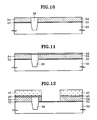
- Figs. 1 and 2 are cross sectional views for explaining the conventional LOCOS isolation method.
- a pad oxide layer 3 and a silicon nitride layer 5 are stacked on a semiconductor substrate 1 and then silicon nitride layer 5 in an inactive region 9 is removed by photo-lithography. Thereafter, channel stopper ions 7 are implanted into inactive region 9 to form separately inactive region 9 and an active region 11.
- Fig. 2 shows a device isolation structure formed by the LOCOS method.
- a channel stopper region 15 where redistribution of impurity ions is realized by thermal diffusion is located under field oxide layer 13.
- pad oxide layer 3 adjacent to inactive region 9 is oxidized in the direction of the active region thereby generating the bird's beak phenomenon. Accordingly, the length 20 of the inactive region becomes greater than that of initial inactive region 17 by a bird's beak generation region 19.
- the bird's beak phenomenon restricts the limit of a design rule for forming a micro pattern, and thereby is a hindrance in the high integration of a semiconductor.
- the field oxide layer is thermally grown up to a thickness of about 5,000 ⁇ and crystal defects are generated by the stress at a boundary of the active region under the silicon nitride layer which is selectively covered on the semiconductor substrate, so leakage current between devices increases.
- Figs. 3 to 6 are cross sectional views according to process order for explaining the conventional trench isolation method.
- a pad oxide layer 2 of about 240 ⁇ is formed on semiconductor substrate 1 and then the silicon nitride layer 4 of about 1,500 ⁇ is formed by low-pressure chemical vapor deposition (LPCVD) and then in sequence a thermal oxide layer 6 of about 1,000 ⁇ is formed, then the thermal oxide layer of the inactive region is removed by a photolithography process.
- LPCVD low-pressure chemical vapor deposition
- nitride layer 4 and pad oxide layer 2 are reactive-ion-etched using the thermal oxide layer remaining on the active region as an etching mask, and then semiconductor substrate 1 is etched by dry etching to form a trench.
- the thermal oxide layer, the etching mask is etched together with the nitride layer, the pad oxide layer and the trench according to an etching selection ratio, so that a little amount of the thermal oxide layer remain.
- the trenches of a narrow region and a wide region coexist in the semiconductor substrate according to the design rule of the semiconductor device.
- a side wall oxide layer 8 is formed inside the trench by the thermal oxidation method, and polycrystalline silicon 10 is deposited to a thickness of 5,000 ⁇ or more, and is etched anisotropically in order to fill the polycrystalline silicon only in the trench.
- polycrystalline silicon 10 is deposited to a thickness of 5,000 ⁇ or more, and is etched anisotropically in order to fill the polycrystalline silicon only in the trench.
- a central portion of the trench of the wide region is depressed to generate a kind of loading effect, so that a filling profile differs according to the size of the trench region.
- a field oxide layer 12 is formed on the polycrystalline silicon filling the trench by the thermal oxidation method.
- the depressed portion of the trench of the wide region is not planarized.
- buffered oxide etchant a mixed solution of ammonium fluoride (NH 4 F) and hydrogen fluoride (HF) in a ratio of 7:1 and phosphoric acid solution
- a sacrifice oxide layer (not shown) is grown up, and then the grown up sacrifice oxide layer is wet-etched again to finish the device isolation process.
- a gate line and a bit line may be shorted, or a wiring characteristic deteriorated, during a subsequent process due to the depressed phenomenon (G) of the polycrystalline silicon of the central portion of the trench of the wide region, resulting in the decrease of yield.
- CMP chemical-mechanical polishing
- the CMP method since the insulating material overfilling the trench is removed in the horizontal direction, the CMP method has been considered as an ideal method for completely filling the trench and thereafter etching the insulating material overfilling the trench.
- the width of the trench becomes on the order of several millimeters, a dishing phenomenon in which the central portion of the wide trench region is depressed in a dish shape, is generated to cause an unstable device isolation characteristic and a structural step difference.
- an isolation method of a semiconductor device comprising the steps of: forming a first device isolation layer in a first inactive region of a semiconductor substrate, by a trench isolation method; and forming a second device isolation layer in a second inactive region which is wider than the first inactive region, by a local oxidation method.
- the boundary of the first and second device isolation layers is formed of a bird's beak region generated during the formation of the second device isolation layer.
- an isolation method of a semiconductor device including the steps of: forming a first pattern on a semiconductor substrate to expose a first inactive region of said substrate; etching the exposed semiconductor substrate by the first pattern to form a trench; forming a first device isolation layer by filling insulating material in the trench; forming a second pattern on the semiconductor substrate to expose a second inactive region of the substrate; and forming a second device isolation layer in the second inactive region by the local oxidation method.
- a CMP or reactive ion etching (RIE) step may be further included for etching back the first device isolation layer after the step of forming the first device isolation layer.
- RIE reactive ion etching
- the bird's beak which is generated during the local oxidation for forming the second inactive region, shares a boundary with the trench.
- the first inactive region exists in the cell array portion and the second inactive region exists in the peripheral circuit portion. It is further preferable that the first device isolation layer is formed of a CVD oxide layer.
- the isolation method of a semiconductor device of the present invention dishing can be prevented and proper device isolation can be achieved without exposure of the active region between the first and second isolation layers.
- a device isolation method by the present invention includes the steps of: (a) forming a first device isolation layer by a trench isolation method on a narrow inactive region and then (B) forming a second device isolation layer on a wide inactive region by the LOCOS isolation method.
- Figs. 7-14 are cross-sectional views for illustrating one embodiment according to process order in order to explain the device isolation method of the semiconductor device by the present invention.
- Fig. 7 is a cross sectional view for illustrating a step of forming a pad oxide layer 32 and a first silicon nitride layer 34 on a semiconductor substrate 30, which includes a first step of forming pad oxide layer 32 on semiconductor substrate 30 and a second step of stacking a first silicon nitride layer 34 on pad oxide layer 32.
- pad oxide layer 32 is formed to a thickness of, for example, about l10 ⁇ -240 ⁇ by a thermal oxidation method and first silicon nitride layer 34 is formed to a thickness of 1,500 ⁇ -2,500 ⁇ by, for example, a chemical vapor deposition (CVD) method.
- CVD chemical vapor deposition
- Fig. 8 shows a photolithography step for defining the inactive region of the cell array portion, which includes a first step of forming a first photoresist pattern 36 on first silicon nitride layer 34 and a second step of etching the first silicon nitride layer and the pad oxide layer by using first photoresist pattern 36 as an etching mask.
- first photoresist pattern 36 is formed to have a shape for exposing the semiconductor substrate of the cell array portion, first silicon nitride layer 34 on the cell array portion is removed by an anisotropic dry etching and pad oxide layer 32 is etched by the reactive ion etching or the wet etching.
- Fig. 9 shows a step of forming a trench 37 in the semiconductor substrate of the inactive region of the cell array portion.
- first photoresist pattern on the first silicon nitride layer is removed and the semiconductor substrate is etched to have a depth of about 2,000 ⁇ -4,000 ⁇ by using first silicon nitride layer as the etching mask to thereby form trench 37.
- first photoresist pattern (represented as a reference numeral 36 of Fig. 8) may be used as the etching mask.
- Fig. 10 shows a step of forming a first device isolation layer 38 by filling the trench, which includes a first step of filling the trench with insulating material and a second step of performing CMP over the whole surface of the resultant having trench filled with insulating material.
- an oxide layer is deposited on the substrate on which the trench is formed by, for example, a CVD method, and then a CMP process is carried out over the whole surface of the resultant having oxide layer thereon until the surface of the first silicon nitride layer 34 is exposed in order to form the oxide layer only inside the trench.
- RIE reactive ion etching
- the thickness of the CVD oxide layer deposited for filling the trench is at most about 4,000 ⁇ , which is very profitable in terms of process time and process margin in comparison with the thickness of about 5,000 ⁇ -10,000 ⁇ of oxide layer used for filling the trench in a conventional device isolation method using only the trench. Also, since only a narrow trench is formed on the semiconductor substrate and then the oxide layer is deposited, a surface of the substrate planarizes wholly such as not to generate a conventional dishing phenomenon even when a subsequent CMP process is carried out.
- the trench isolation is thus realized in the cell array portion by processes from Fig. 7 to Fig. 10.
- Fig. 11 shows a step of forming a second silicon nitride layer 40.
- silicon nitride layer 40 is deposited on the substrate in which first device isolation layer 38 is formed, to a thickness of, for example, 300 ⁇ -700 ⁇ , which is sufficient to protect the trench portion from an oxidation atmosphere at high temperature, thereby to form second silicon nitride layer 40.
- second silicon nitride layer 40 has a purpose of prevention of change in electrical characteristic or size which could be caused by oxidation of the trench in a high temperature oxidation atmosphere.
- Fig. 12 shows a step of defining the inactive region for isolating the peripheral portion of the semiconductor substrate by a photolithography process.
- This includes a first step of coating photoresist on second silicon nitride layer 40; the coated photoresist is then patterned to form a second photoresist pattern 42 for exposing the silicon nitride layer on the inactive region of the peripheral portion. It also includes a second step of etching second silicon nitride layer 40 by using the second photoresist pattern as an etching mask and a third step of etching first silicon nitride layer 34 to expose the pad oxide layer on the inactive region of the peripheral portion.
- a misalign margin of the photolithography process is a length "C" as shown in Fig. 13.
- a bird's beak generated during a subsequent local oxidation should form the boundary of the trench filling oxide layer and the thermal oxide layer and this boundary should be located within "C" portion. Accordingly, the length of the bird's beak becomes the misalign margin of the photolithography process.
- the length of the bird's beak generated by the local oxidation ranges from 5,000 ⁇ to 10,000 ⁇ . Accordingly, even though taking into account the situation that the misalign of the photolithography process of a high integration semiconductor device is comparatively loosened 2,000 ⁇ , "C" portion of the present invention can be a sufficient margin in the photolithography process.
- Fig. 13 shows a step of forming a second device isolation layer 46 in the inactive region of the peripheral portion.
- second device isolation layer 46 is formed in the inactive region of the peripheral portion, namely, a region where the pad oxide layer is exposed by the photolithography process of Fig. 12, by thermal oxidation at high temperature.
- device isolation is realized in the peripheral portion with the thermal oxide layer by the local oxidation, and the active region is not exposed at the boundary of the trench due to the bird's beak generated during forming the thermal oxide layer.
- the second silicon nitride layer plays a role in protecting the trench portion from the oxidation atmosphere during the oxidation process.
- Fig. 14 shows a step of completing the device isolation by the LOCOS and the trench isolation method of the present invention.
- the second silicon nitride layer and the first silicon nitride layer are removed by using a wet etching method and then the pad oxide layer is etched by a wet etching method and removed to complete the device isolation process.
- first device isolation layer 38 filled in the trench and second device isolation layer 46 formed by the local oxidation is formed from the thermal oxidation layer, whose etching ratio is lower than that of the CVD oxide layer filled in the trench, at the time of the wet etching process for removing the pad oxide layer, and thus device isolation can be realized without the exposure of the active region.
- the device isolation layer by the trench method is formed in a narrow portion and CMP is carried out, so that no dishing phenomenon is generated. Moreover, after the trench isolation process, the device isolation layer is formed in a wide portion by local oxidation so that device isolation can be realized without the exposure of the active region at the boundary of the two device isolation layers, thereby improving the electrical characteristic of the device.
Landscapes
- Element Separation (AREA)
- Local Oxidation Of Silicon (AREA)
Applications Claiming Priority (2)
| Application Number | Priority Date | Filing Date | Title |
|---|---|---|---|
| KR9509455 | 1995-04-21 | ||
| KR1019950009455A KR0147630B1 (ko) | 1995-04-21 | 1995-04-21 | 반도체 장치의 소자분리방법 |
Publications (3)
| Publication Number | Publication Date |
|---|---|
| EP0739032A2 true EP0739032A2 (de) | 1996-10-23 |
| EP0739032A3 EP0739032A3 (de) | 1997-10-29 |
| EP0739032B1 EP0739032B1 (de) | 2005-05-04 |
Family
ID=19412675
Family Applications (1)
| Application Number | Title | Priority Date | Filing Date |
|---|---|---|---|
| EP96301226A Expired - Lifetime EP0739032B1 (de) | 1995-04-21 | 1996-02-23 | Verfahren zur Isolierung einer Halbleiteranordnung |
Country Status (5)
| Country | Link |
|---|---|
| US (1) | US5728620A (de) |
| EP (1) | EP0739032B1 (de) |
| JP (1) | JPH08293541A (de) |
| KR (1) | KR0147630B1 (de) |
| DE (1) | DE69634675T2 (de) |
Families Citing this family (23)
| Publication number | Priority date | Publication date | Assignee | Title |
|---|---|---|---|---|
| KR970023978A (ko) * | 1995-10-04 | 1997-05-30 | 김주용 | 반도체 소자의 평탄된 소자분리막 제조 방법 |
| US5858842A (en) * | 1996-07-03 | 1999-01-12 | Samsung Electronics Co., Ltd. | Methods of forming combined trench and locos-based electrical isolation regions in semiconductor substrates |
| JPH10144785A (ja) * | 1996-11-06 | 1998-05-29 | Samsung Electron Co Ltd | 半導体装置及びその素子分離方法 |
| US5897356A (en) * | 1997-02-27 | 1999-04-27 | Micron Technology, Inc. | Methods of forming field oxide and active area regions on a semiconductive substrate |
| US5858830A (en) * | 1997-06-12 | 1999-01-12 | Taiwan Semiconductor Manufacturing Company, Ltd. | Method of making dual isolation regions for logic and embedded memory devices |
| KR100253078B1 (ko) | 1997-12-23 | 2000-04-15 | 윤종용 | 반도체 장치의 트렌치 격리 형성 방법 |
| US6004862A (en) * | 1998-01-20 | 1999-12-21 | Advanced Micro Devices, Inc. | Core array and periphery isolation technique |
| TW449900B (en) * | 1998-05-26 | 2001-08-11 | United Microelectronics Corp | Method to define dummy patterns |
| KR100286736B1 (ko) | 1998-06-16 | 2001-04-16 | 윤종용 | 트렌치 격리 형성 방법 |
| US6372601B1 (en) | 1998-09-03 | 2002-04-16 | Micron Technology, Inc. | Isolation region forming methods |
| US6274498B1 (en) * | 1998-09-03 | 2001-08-14 | Micron Technology, Inc. | Methods of forming materials within openings, and method of forming isolation regions |
| US6149830A (en) * | 1998-09-17 | 2000-11-21 | Siemens Aktiengesellschaft | Composition and method for reducing dishing in patterned metal during CMP process |
| US6528389B1 (en) | 1998-12-17 | 2003-03-04 | Lsi Logic Corporation | Substrate planarization with a chemical mechanical polishing stop layer |
| KR20000041419A (ko) * | 1998-12-22 | 2000-07-15 | 김영환 | 트렌치 형성 공정 및 로코스 공정을 이용한 반도체 소자의 소자분리막 형성 방법 |
| US6300220B1 (en) * | 2000-01-06 | 2001-10-09 | National Semiconductor Corporation | Process for fabricating isolation structure for IC featuring grown and buried field oxide |
| JP2001230315A (ja) * | 2000-02-17 | 2001-08-24 | Mitsubishi Electric Corp | 半導体装置およびその製造方法 |
| US6465324B2 (en) * | 2001-03-23 | 2002-10-15 | Honeywell International Inc. | Recessed silicon oxidation for devices such as a CMOS SOI ICs |
| JP2009182114A (ja) * | 2008-01-30 | 2009-08-13 | Elpida Memory Inc | 半導体装置およびその製造方法 |
| JP2009272480A (ja) * | 2008-05-08 | 2009-11-19 | Nec Electronics Corp | 半導体装置の製造方法 |
| US20090311868A1 (en) * | 2008-06-16 | 2009-12-17 | Nec Electronics Corporation | Semiconductor device manufacturing method |
| US8211778B2 (en) * | 2008-12-23 | 2012-07-03 | Micron Technology, Inc. | Forming isolation regions for integrated circuits |
| US8680617B2 (en) * | 2009-10-06 | 2014-03-25 | International Business Machines Corporation | Split level shallow trench isolation for area efficient body contacts in SOI MOSFETS |
| CN102709227A (zh) * | 2012-06-21 | 2012-10-03 | 上海华力微电子有限公司 | 浅沟槽隔离平坦化方法以及半导体制造方法 |
Family Cites Families (11)
| Publication number | Priority date | Publication date | Assignee | Title |
|---|---|---|---|---|
| US4394196A (en) * | 1980-07-16 | 1983-07-19 | Tokyo Shibaura Denki Kabushiki Kaisha | Method of etching, refilling and etching dielectric grooves for isolating micron size device regions |
| JPH077794B2 (ja) * | 1984-07-11 | 1995-01-30 | 株式会社日立製作所 | 半導体集積回路装置の製造方法 |
| FR2598557B1 (fr) * | 1986-05-09 | 1990-03-30 | Seiko Epson Corp | Procede de fabrication d'une region d'isolation d'element d'un dispositif a semi-conducteurs |
| US4892614A (en) * | 1986-07-07 | 1990-01-09 | Texas Instruments Incorporated | Integrated circuit isolation process |
| US4980311A (en) * | 1987-05-05 | 1990-12-25 | Seiko Epson Corporation | Method of fabricating a semiconductor device |
| JPH01215036A (ja) * | 1988-02-24 | 1989-08-29 | Seiko Epson Corp | 半導体集積回路装置 |
| US4942137A (en) * | 1989-08-14 | 1990-07-17 | Motorola, Inc. | Self-aligned trench with selective trench fill |
| US4994406A (en) * | 1989-11-03 | 1991-02-19 | Motorola Inc. | Method of fabricating semiconductor devices having deep and shallow isolation structures |
| JP2597022B2 (ja) * | 1990-02-23 | 1997-04-02 | シャープ株式会社 | 素子分離領域の形成方法 |
| US5130268A (en) * | 1991-04-05 | 1992-07-14 | Sgs-Thomson Microelectronics, Inc. | Method for forming planarized shallow trench isolation in an integrated circuit and a structure formed thereby |
| JPH0574927A (ja) * | 1991-09-13 | 1993-03-26 | Nec Corp | 半導体装置の製造方法 |
-
1995
- 1995-04-21 KR KR1019950009455A patent/KR0147630B1/ko not_active Expired - Fee Related
-
1996
- 1996-01-25 US US08/591,826 patent/US5728620A/en not_active Expired - Lifetime
- 1996-02-23 DE DE69634675T patent/DE69634675T2/de not_active Expired - Lifetime
- 1996-02-23 EP EP96301226A patent/EP0739032B1/de not_active Expired - Lifetime
- 1996-02-28 JP JP8041380A patent/JPH08293541A/ja active Pending
Also Published As
| Publication number | Publication date |
|---|---|
| KR960039276A (ko) | 1996-11-21 |
| EP0739032A3 (de) | 1997-10-29 |
| US5728620A (en) | 1998-03-17 |
| JPH08293541A (ja) | 1996-11-05 |
| KR0147630B1 (ko) | 1998-11-02 |
| EP0739032B1 (de) | 2005-05-04 |
| DE69634675T2 (de) | 2006-01-19 |
| DE69634675D1 (de) | 2005-06-09 |
Similar Documents
| Publication | Publication Date | Title |
|---|---|---|
| EP0739032B1 (de) | Verfahren zur Isolierung einer Halbleiteranordnung | |
| US5807784A (en) | Device isolation methods for a semiconductor device | |
| US6187651B1 (en) | Methods of forming trench isolation regions using preferred stress relieving layers and techniques to inhibit the occurrence of voids | |
| KR100213196B1 (ko) | 트렌치 소자분리 | |
| US7807532B2 (en) | Method and structure for self aligned formation of a gate polysilicon layer | |
| US7033909B2 (en) | Method of forming trench isolations | |
| US7858492B2 (en) | Method of filling a trench and method of forming an isolating layer structure using the same | |
| US6071792A (en) | Methods of forming shallow trench isolation regions using plasma deposition techniques | |
| US5604149A (en) | Method of and device for isolating active areas of a semiconducor substrate by quasi-plane shallow trenches | |
| US6335287B1 (en) | Method of forming trench isolation regions | |
| US5453395A (en) | Isolation technology using liquid phase deposition | |
| US6331472B1 (en) | Method for forming shallow trench isolation | |
| US20020004284A1 (en) | Method for forming a shallow trench isolation structure including a dummy pattern in the wider trench | |
| US20050023634A1 (en) | Method of fabricating shallow trench isolation structure and microelectronic device having the structure | |
| US5641704A (en) | Method of isolating active areas of a semiconductor substrate by shallow trenches and narrow trenches | |
| US6008526A (en) | Device isolation layer for a semiconductor device | |
| US20020072196A1 (en) | Shallow trench isolation for thin silicon/silicon-on-insulator substrates by utilizing polysilicon | |
| JP2000164690A (ja) | 半導体装置の製造方法 | |
| KR20010008579A (ko) | 반도체장치의 sti형 소자분리막 형성방법 | |
| US6444539B1 (en) | Method for producing a shallow trench isolation filled with thermal oxide | |
| US6323105B1 (en) | Method for fabricating an isolation structure including a shallow trench isolation structure and a local-oxidation isolation structure | |
| US6991993B2 (en) | Method of fabricating trench isolation structure of a semiconductor device | |
| KR100954418B1 (ko) | 반도체 소자의 소자분리막 형성방법 | |
| US6423612B1 (en) | Method of fabricating a shallow trench isolation structure with reduced topography | |
| KR100214530B1 (ko) | 트렌치 소자격리구조 형성방법 |
Legal Events
| Date | Code | Title | Description |
|---|---|---|---|
| PUAI | Public reference made under article 153(3) epc to a published international application that has entered the european phase |
Free format text: ORIGINAL CODE: 0009012 |
|
| AK | Designated contracting states |
Kind code of ref document: A2 Designated state(s): DE FR GB |
|
| PUAL | Search report despatched |
Free format text: ORIGINAL CODE: 0009013 |
|
| AK | Designated contracting states |
Kind code of ref document: A3 Designated state(s): DE FR GB |
|
| 17P | Request for examination filed |
Effective date: 19980414 |
|
| 17Q | First examination report despatched |
Effective date: 20020429 |
|
| GRAP | Despatch of communication of intention to grant a patent |
Free format text: ORIGINAL CODE: EPIDOSNIGR1 |
|
| GRAS | Grant fee paid |
Free format text: ORIGINAL CODE: EPIDOSNIGR3 |
|
| GRAA | (expected) grant |
Free format text: ORIGINAL CODE: 0009210 |
|
| AK | Designated contracting states |
Kind code of ref document: B1 Designated state(s): DE FR GB |
|
| REG | Reference to a national code |
Ref country code: GB Ref legal event code: FG4D |
|
| REF | Corresponds to: |
Ref document number: 69634675 Country of ref document: DE Date of ref document: 20050609 Kind code of ref document: P |
|
| PLBE | No opposition filed within time limit |
Free format text: ORIGINAL CODE: 0009261 |
|
| STAA | Information on the status of an ep patent application or granted ep patent |
Free format text: STATUS: NO OPPOSITION FILED WITHIN TIME LIMIT |
|
| ET | Fr: translation filed | ||
| 26N | No opposition filed |
Effective date: 20060207 |
|
| PGFP | Annual fee paid to national office [announced via postgrant information from national office to epo] |
Ref country code: FR Payment date: 20100324 Year of fee payment: 15 |
|
| PGFP | Annual fee paid to national office [announced via postgrant information from national office to epo] |
Ref country code: GB Payment date: 20100128 Year of fee payment: 15 Ref country code: DE Payment date: 20100202 Year of fee payment: 15 |
|
| GBPC | Gb: european patent ceased through non-payment of renewal fee |
Effective date: 20110223 |
|
| REG | Reference to a national code |
Ref country code: FR Ref legal event code: ST Effective date: 20111102 |
|
| REG | Reference to a national code |
Ref country code: DE Ref legal event code: R119 Ref document number: 69634675 Country of ref document: DE Effective date: 20110901 |
|
| PG25 | Lapsed in a contracting state [announced via postgrant information from national office to epo] |
Ref country code: FR Free format text: LAPSE BECAUSE OF NON-PAYMENT OF DUE FEES Effective date: 20110228 |
|
| PG25 | Lapsed in a contracting state [announced via postgrant information from national office to epo] |
Ref country code: GB Free format text: LAPSE BECAUSE OF NON-PAYMENT OF DUE FEES Effective date: 20110223 |
|
| PG25 | Lapsed in a contracting state [announced via postgrant information from national office to epo] |
Ref country code: DE Free format text: LAPSE BECAUSE OF NON-PAYMENT OF DUE FEES Effective date: 20110901 |