EP0736902A2 - Dispositif à circuit intégré et procédé de fabrication - Google Patents
Dispositif à circuit intégré et procédé de fabrication Download PDFInfo
- Publication number
- EP0736902A2 EP0736902A2 EP96100652A EP96100652A EP0736902A2 EP 0736902 A2 EP0736902 A2 EP 0736902A2 EP 96100652 A EP96100652 A EP 96100652A EP 96100652 A EP96100652 A EP 96100652A EP 0736902 A2 EP0736902 A2 EP 0736902A2
- Authority
- EP
- European Patent Office
- Prior art keywords
- magnetic substance
- thermoplastic material
- bias line
- layer
- integrated circuit
- Prior art date
- Legal status (The legal status is an assumption and is not a legal conclusion. Google has not performed a legal analysis and makes no representation as to the accuracy of the status listed.)
- Granted
Links
Images


Classifications
-
- H—ELECTRICITY
- H01—ELECTRIC ELEMENTS
- H01L—SEMICONDUCTOR DEVICES NOT COVERED BY CLASS H10
- H01L27/00—Devices consisting of a plurality of semiconductor or other solid-state components formed in or on a common substrate
- H01L27/02—Devices consisting of a plurality of semiconductor or other solid-state components formed in or on a common substrate including semiconductor components specially adapted for rectifying, oscillating, amplifying or switching and having at least one potential-jump barrier or surface barrier; including integrated passive circuit elements with at least one potential-jump barrier or surface barrier
- H01L27/04—Devices consisting of a plurality of semiconductor or other solid-state components formed in or on a common substrate including semiconductor components specially adapted for rectifying, oscillating, amplifying or switching and having at least one potential-jump barrier or surface barrier; including integrated passive circuit elements with at least one potential-jump barrier or surface barrier the substrate being a semiconductor body
- H01L27/06—Devices consisting of a plurality of semiconductor or other solid-state components formed in or on a common substrate including semiconductor components specially adapted for rectifying, oscillating, amplifying or switching and having at least one potential-jump barrier or surface barrier; including integrated passive circuit elements with at least one potential-jump barrier or surface barrier the substrate being a semiconductor body including a plurality of individual components in a non-repetitive configuration
- H01L27/0605—Devices consisting of a plurality of semiconductor or other solid-state components formed in or on a common substrate including semiconductor components specially adapted for rectifying, oscillating, amplifying or switching and having at least one potential-jump barrier or surface barrier; including integrated passive circuit elements with at least one potential-jump barrier or surface barrier the substrate being a semiconductor body including a plurality of individual components in a non-repetitive configuration integrated circuits made of compound material, e.g. AIIIBV
-
- H—ELECTRICITY
- H01—ELECTRIC ELEMENTS
- H01L—SEMICONDUCTOR DEVICES NOT COVERED BY CLASS H10
- H01L23/00—Details of semiconductor or other solid state devices
- H01L23/58—Structural electrical arrangements for semiconductor devices not otherwise provided for, e.g. in combination with batteries
- H01L23/64—Impedance arrangements
- H01L23/66—High-frequency adaptations
-
- H—ELECTRICITY
- H03—ELECTRONIC CIRCUITRY
- H03F—AMPLIFIERS
- H03F1/00—Details of amplifiers with only discharge tubes, only semiconductor devices or only unspecified devices as amplifying elements
- H03F1/08—Modifications of amplifiers to reduce detrimental influences of internal impedances of amplifying elements
- H03F1/083—Modifications of amplifiers to reduce detrimental influences of internal impedances of amplifying elements in transistor amplifiers
-
- H—ELECTRICITY
- H01—ELECTRIC ELEMENTS
- H01L—SEMICONDUCTOR DEVICES NOT COVERED BY CLASS H10
- H01L2223/00—Details relating to semiconductor or other solid state devices covered by the group H01L23/00
- H01L2223/58—Structural electrical arrangements for semiconductor devices not otherwise provided for
- H01L2223/64—Impedance arrangements
- H01L2223/66—High-frequency adaptations
- H01L2223/6644—Packaging aspects of high-frequency amplifiers
- H01L2223/665—Bias feed arrangements
-
- H—ELECTRICITY
- H01—ELECTRIC ELEMENTS
- H01L—SEMICONDUCTOR DEVICES NOT COVERED BY CLASS H10
- H01L2924/00—Indexing scheme for arrangements or methods for connecting or disconnecting semiconductor or solid-state bodies as covered by H01L24/00
- H01L2924/0001—Technical content checked by a classifier
- H01L2924/0002—Not covered by any one of groups H01L24/00, H01L24/00 and H01L2224/00
-
- H—ELECTRICITY
- H01—ELECTRIC ELEMENTS
- H01L—SEMICONDUCTOR DEVICES NOT COVERED BY CLASS H10
- H01L2924/00—Indexing scheme for arrangements or methods for connecting or disconnecting semiconductor or solid-state bodies as covered by H01L24/00
- H01L2924/19—Details of hybrid assemblies other than the semiconductor or other solid state devices to be connected
- H01L2924/191—Disposition
- H01L2924/19101—Disposition of discrete passive components
- H01L2924/19105—Disposition of discrete passive components in a side-by-side arrangement on a common die mounting substrate
Definitions
- thermoplastic material layer is formed on a region of the substrate including a required region on the bias line. Therefore, after evaluating the oscillation characteristics of the active element, the magnetic substance layer can be formed in an appropriate shape and at an appropriate position on the bias line so that the oscillation of the active element is stopped. Further, the unwanted increase in the chip area of the integrated circuit device due to the use of the prior art oscillation preventing circuit is avoided.
- a microwave signal applied to the input electrode pad 21 is transmitted through the MIM capacitor 4 and the signal transmission line 51 to the gate of the transistor 7.
- An output signal from the drain of the transistor 7 is transmitted through the signal transmission line 52 to a subsequent stage circuit (not shown).
- a gate bias voltage applied to the gate bias electrode pad 23 is transmitted through the gate side bias line 61 and the signal transmission line 51 to the gate of the transistor 7, and a drain bias voltage applied to the drain bias electrode pad 24 is transmitted through the drain side bias line 62 and the signal transmission line 52 to the drain of the transistor 7.
- the via-holes 3 connect the ground electrode pads 22 to a metal layer (not shown) on the rear surface of the semiconductor substrate 1.
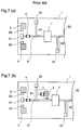
- FIG 5 is a plan view illustrating a monolithic microwave semiconductor IC device in accordance with a third embodiment of the present invention.
- the same reference numerals as those in figure 1 designate the same or corresponding parts.
- Reference numeral 10 designates island patterns of thermoplastic polyimide (hereinafter referred to as thermoplastic polyimide patterns).
Priority Applications (1)
| Application Number | Priority Date | Filing Date | Title |
|---|---|---|---|
| EP00117641A EP1059666A1 (fr) | 1995-04-05 | 1996-01-17 | Dispositif à circuit intégré à semiconducteur monolithique |
Applications Claiming Priority (3)
| Application Number | Priority Date | Filing Date | Title |
|---|---|---|---|
| JP8022195 | 1995-04-05 | ||
| JP80221/95 | 1995-04-05 | ||
| JP7080221A JPH08279596A (ja) | 1995-04-05 | 1995-04-05 | 集積回路装置,及びその製造方法 |
Related Child Applications (1)
| Application Number | Title | Priority Date | Filing Date |
|---|---|---|---|
| EP00117641.1 Division-Into | 2000-08-16 |
Publications (3)
| Publication Number | Publication Date |
|---|---|
| EP0736902A2 true EP0736902A2 (fr) | 1996-10-09 |
| EP0736902A3 EP0736902A3 (fr) | 1997-10-29 |
| EP0736902B1 EP0736902B1 (fr) | 2001-09-26 |
Family
ID=13712321
Family Applications (2)
| Application Number | Title | Priority Date | Filing Date |
|---|---|---|---|
| EP00117641A Withdrawn EP1059666A1 (fr) | 1995-04-05 | 1996-01-17 | Dispositif à circuit intégré à semiconducteur monolithique |
| EP96100652A Expired - Lifetime EP0736902B1 (fr) | 1995-04-05 | 1996-01-17 | Dispositif à circuit intégré et procédé de fabrication |
Family Applications Before (1)
| Application Number | Title | Priority Date | Filing Date |
|---|---|---|---|
| EP00117641A Withdrawn EP1059666A1 (fr) | 1995-04-05 | 1996-01-17 | Dispositif à circuit intégré à semiconducteur monolithique |
Country Status (4)
| Country | Link |
|---|---|
| US (1) | US5675184A (fr) |
| EP (2) | EP1059666A1 (fr) |
| JP (1) | JPH08279596A (fr) |
| DE (1) | DE69615437T2 (fr) |
Cited By (2)
| Publication number | Priority date | Publication date | Assignee | Title |
|---|---|---|---|---|
| EP0739034A2 (fr) * | 1995-04-20 | 1996-10-23 | Mitsubishi Denki Kabushiki Kaisha | Dispositif de circuit intégré à semi-conducteur et procédé de fabrication |
| WO2003054959A3 (fr) * | 2001-12-20 | 2004-04-29 | Eupec Gmbh & Co Kg | Circuit comportant des composants electroniques loges sur un substrat support isolant |
Families Citing this family (33)
| Publication number | Priority date | Publication date | Assignee | Title |
|---|---|---|---|---|
| JP3185918B2 (ja) * | 1996-08-05 | 2001-07-11 | 株式会社村田製作所 | 電子装置 |
| US6329234B1 (en) | 2000-07-24 | 2001-12-11 | Taiwan Semiconductor Manufactuirng Company | Copper process compatible CMOS metal-insulator-metal capacitor structure and its process flow |
| JP4804643B2 (ja) * | 2001-05-08 | 2011-11-02 | 三菱電機株式会社 | 高周波回路装置とその製造方法 |
| US7091542B1 (en) * | 2005-01-28 | 2006-08-15 | International Business Machines Corporation | Method of forming a MIM capacitor for Cu BEOL application |
| US20060197183A1 (en) * | 2005-03-01 | 2006-09-07 | International Business Machines Corporation | Improved mim capacitor structure and process |
| US7223654B2 (en) * | 2005-04-15 | 2007-05-29 | International Business Machines Corporation | MIM capacitor and method of fabricating same |
| US7942874B2 (en) | 2005-05-12 | 2011-05-17 | Aragon Surgical, Inc. | Apparatus for tissue cauterization |
| US8728072B2 (en) | 2005-05-12 | 2014-05-20 | Aesculap Ag | Electrocautery method and apparatus |
| US9339323B2 (en) | 2005-05-12 | 2016-05-17 | Aesculap Ag | Electrocautery method and apparatus |
| US8696662B2 (en) | 2005-05-12 | 2014-04-15 | Aesculap Ag | Electrocautery method and apparatus |
| US8574229B2 (en) | 2006-05-02 | 2013-11-05 | Aesculap Ag | Surgical tool |
| JP5078471B2 (ja) * | 2007-07-06 | 2012-11-21 | 三菱電機株式会社 | 高周波増幅器 |
| US8870867B2 (en) | 2008-02-06 | 2014-10-28 | Aesculap Ag | Articulable electrosurgical instrument with a stabilizable articulation actuator |
| KR101580925B1 (ko) * | 2009-04-28 | 2015-12-30 | 삼성전자주식회사 | 칩온 보드 타입의 패키지 |
| WO2011097469A2 (fr) | 2010-02-04 | 2011-08-11 | Aragon Surgical, Inc. | Dispositif pour chirurgie laparoscopique à radiofréquence |
| US8827992B2 (en) | 2010-03-26 | 2014-09-09 | Aesculap Ag | Impedance mediated control of power delivery for electrosurgery |
| US8419727B2 (en) | 2010-03-26 | 2013-04-16 | Aesculap Ag | Impedance mediated power delivery for electrosurgery |
| US9173698B2 (en) | 2010-09-17 | 2015-11-03 | Aesculap Ag | Electrosurgical tissue sealing augmented with a seal-enhancing composition |
| US8405135B2 (en) | 2010-10-05 | 2013-03-26 | International Business Machines Corporation | 3D via capacitor with a floating conductive plate for improved reliability |
| US9339327B2 (en) | 2011-06-28 | 2016-05-17 | Aesculap Ag | Electrosurgical tissue dissecting device |
| ES2660397T3 (es) | 2012-09-26 | 2018-03-22 | Aesculap Ag | Aparato para corte y sellado de tejido |
| US8901711B1 (en) | 2013-08-07 | 2014-12-02 | International Business Machines Corporation | Horizontal metal-insulator-metal capacitor |
| US10090240B2 (en) | 2016-06-03 | 2018-10-02 | Globalfoundries Inc. | Interconnect structure with capacitor element and related methods |
| US9875959B2 (en) | 2016-06-09 | 2018-01-23 | International Business Machines Corporation | Forming a stacked capacitor |
| US10032711B2 (en) | 2016-07-25 | 2018-07-24 | International Business Machines Corporation | Integrating metal-insulator-metal capacitors with air gap process flow |
| US9893144B1 (en) | 2016-08-05 | 2018-02-13 | International Business Machines Corporation | Methods for fabricating metal-insulator-metal capacitors |
| US9698213B1 (en) | 2016-09-28 | 2017-07-04 | International Business Machines Corporation | Vertical MIM capacitor |
| US9876068B1 (en) | 2016-10-31 | 2018-01-23 | International Business Machines Corporation | High-K metal-insulator-metal capacitor and method of manufacturing the same |
| US10008558B1 (en) | 2017-01-05 | 2018-06-26 | International Business Machines Corporation | Advanced metal insulator metal capacitor |
| US10032855B1 (en) | 2017-01-05 | 2018-07-24 | International Business Machines Corporation | Advanced metal insulator metal capacitor |
| US10090378B1 (en) | 2017-03-17 | 2018-10-02 | International Business Machines Corporation | Efficient metal-insulator-metal capacitor |
| US11031457B2 (en) | 2017-12-15 | 2021-06-08 | International Business Machines Corporation | Low resistance high capacitance density MIM capacitor |
| US10497519B1 (en) | 2018-09-27 | 2019-12-03 | International Business Machines Corporation | Back-end-of-the line capacitor |
Citations (6)
| Publication number | Priority date | Publication date | Assignee | Title |
|---|---|---|---|---|
| JPS5797201A (en) * | 1980-12-09 | 1982-06-16 | Fujitsu Ltd | Integrated circuit for microwave |
| EP0169694A2 (fr) * | 1984-07-25 | 1986-01-29 | Rca Licensing Corporation | Composant supprimant de signaux à haute fréquence |
| US4716389A (en) * | 1986-10-20 | 1987-12-29 | Honeywell Inc. | Millimeter wave microstrip surface mounted attenuator |
| JPH0352302A (ja) * | 1989-07-19 | 1991-03-06 | Sanyo Electric Co Ltd | モノリシックマイクロ波集積回路 |
| EP0461316A1 (fr) * | 1989-03-28 | 1991-12-18 | General Electric Company | Attachement d'un dé semi-conducteur |
| JPH05235655A (ja) * | 1992-02-19 | 1993-09-10 | Toshiba Lighting & Technol Corp | 高周波用増幅回路 |
Family Cites Families (4)
| Publication number | Priority date | Publication date | Assignee | Title |
|---|---|---|---|---|
| US3959874A (en) * | 1974-12-20 | 1976-06-01 | Western Electric Company, Inc. | Method of forming an integrated circuit assembly |
| US5138431A (en) * | 1990-01-31 | 1992-08-11 | Vlsi Technology, Inc. | Lead and socket structures with reduced self-inductance |
| US5469334A (en) * | 1991-09-09 | 1995-11-21 | Power Integrations, Inc. | Plastic quad-packaged switched-mode integrated circuit with integrated transformer windings and mouldings for transformer core pieces |
| JP3137223B2 (ja) * | 1995-01-20 | 2001-02-19 | 三菱電機株式会社 | 高周波増幅器およびその発振防止方法 |
-
1995
- 1995-04-05 JP JP7080221A patent/JPH08279596A/ja active Pending
-
1996
- 1996-01-17 US US08/587,527 patent/US5675184A/en not_active Expired - Fee Related
- 1996-01-17 EP EP00117641A patent/EP1059666A1/fr not_active Withdrawn
- 1996-01-17 EP EP96100652A patent/EP0736902B1/fr not_active Expired - Lifetime
- 1996-01-17 DE DE69615437T patent/DE69615437T2/de not_active Expired - Fee Related
Patent Citations (6)
| Publication number | Priority date | Publication date | Assignee | Title |
|---|---|---|---|---|
| JPS5797201A (en) * | 1980-12-09 | 1982-06-16 | Fujitsu Ltd | Integrated circuit for microwave |
| EP0169694A2 (fr) * | 1984-07-25 | 1986-01-29 | Rca Licensing Corporation | Composant supprimant de signaux à haute fréquence |
| US4716389A (en) * | 1986-10-20 | 1987-12-29 | Honeywell Inc. | Millimeter wave microstrip surface mounted attenuator |
| EP0461316A1 (fr) * | 1989-03-28 | 1991-12-18 | General Electric Company | Attachement d'un dé semi-conducteur |
| JPH0352302A (ja) * | 1989-07-19 | 1991-03-06 | Sanyo Electric Co Ltd | モノリシックマイクロ波集積回路 |
| JPH05235655A (ja) * | 1992-02-19 | 1993-09-10 | Toshiba Lighting & Technol Corp | 高周波用増幅回路 |
Non-Patent Citations (3)
| Title |
|---|
| PATENT ABSTRACTS OF JAPAN vol. 006, no. 182 (E-131), 18 September 1982 & JP 57 097201 A (FUJITSU LTD), 16 June 1982, * |
| PATENT ABSTRACTS OF JAPAN vol. 015, no. 195 (E-1069), 20 May 1991 & JP 03 052302 A (SANYO ELECTRIC CO LTD), 6 March 1991, * |
| PATENT ABSTRACTS OF JAPAN vol. 017, no. 691 (E-1479), 17 December 1993 & JP 05 235655 A (TOSHIBA LIGHTING & TECHNOL CORP), 10 September 1993, * |
Cited By (3)
| Publication number | Priority date | Publication date | Assignee | Title |
|---|---|---|---|---|
| EP0739034A2 (fr) * | 1995-04-20 | 1996-10-23 | Mitsubishi Denki Kabushiki Kaisha | Dispositif de circuit intégré à semi-conducteur et procédé de fabrication |
| EP0739034A3 (fr) * | 1995-04-20 | 1999-07-14 | Mitsubishi Denki Kabushiki Kaisha | Dispositif de circuit intégré à semi-conducteur et procédé de fabrication |
| WO2003054959A3 (fr) * | 2001-12-20 | 2004-04-29 | Eupec Gmbh & Co Kg | Circuit comportant des composants electroniques loges sur un substrat support isolant |
Also Published As
| Publication number | Publication date |
|---|---|
| JPH08279596A (ja) | 1996-10-22 |
| DE69615437T2 (de) | 2002-07-11 |
| EP0736902A3 (fr) | 1997-10-29 |
| EP1059666A1 (fr) | 2000-12-13 |
| US5675184A (en) | 1997-10-07 |
| DE69615437D1 (de) | 2001-10-31 |
| EP0736902B1 (fr) | 2001-09-26 |
Similar Documents
| Publication | Publication Date | Title |
|---|---|---|
| US5675184A (en) | Integrated circuit device | |
| US5635762A (en) | Flip chip semiconductor device with dual purpose metallized ground conductor | |
| US7323770B2 (en) | Hybrid integrated circuit device, and method for fabricating the same, and electronic device | |
| US5629241A (en) | Microwave/millimeter wave circuit structure with discrete flip-chip mounted elements, and method of fabricating the same | |
| GB2269935A (en) | Compact semiconductor device with moulded body | |
| EP0818823A2 (fr) | Module à radio-fréquence et procédé de fabrication du module à radio-fréquence | |
| JPH045289B2 (fr) | ||
| US6661101B2 (en) | Semiconductor device | |
| US6710426B2 (en) | Semiconductor device and transceiver apparatus | |
| JP3328542B2 (ja) | 高周波半導体集積回路装置 | |
| JP2001044448A (ja) | 電界効果トランジスタ、該電界効果トランジスタを含むモノリシックマイクロ波集積回路、及び設計方法 | |
| JPH06252208A (ja) | 半導体集積回路装置 | |
| JPH02288409A (ja) | 抵抗帰還型増幅器 | |
| JPH01173761A (ja) | 高周波用トランジスタ | |
| US5786627A (en) | Integrated circuit device and fabricating thereof | |
| JPS6348855A (ja) | モノリシツク化マイクロ波集積回路 | |
| JPH02241046A (ja) | 半導体集積回路の製造方法 | |
| JPH10126032A (ja) | 表面実装部品の実装構造及び実装方法 | |
| JP2802375B2 (ja) | 電気素子・光素子混載回路の周波数特性伸張法 | |
| JPH04261206A (ja) | 増幅器 | |
| JP2674546B2 (ja) | ビームリード型半導体装置の製造方法 | |
| JPH03145141A (ja) | 半導体装置 | |
| JPS63133701A (ja) | マイクロ波半導体装置 | |
| JPH05211279A (ja) | 混成集積回路 | |
| JPH0139219B2 (fr) |
Legal Events
| Date | Code | Title | Description |
|---|---|---|---|
| PUAI | Public reference made under article 153(3) epc to a published international application that has entered the european phase |
Free format text: ORIGINAL CODE: 0009012 |
|
| AK | Designated contracting states |
Kind code of ref document: A2 Designated state(s): DE FR GB |
|
| PUAL | Search report despatched |
Free format text: ORIGINAL CODE: 0009013 |
|
| AK | Designated contracting states |
Kind code of ref document: A3 Designated state(s): DE FR GB |
|
| 17P | Request for examination filed |
Effective date: 19971211 |
|
| 17Q | First examination report despatched |
Effective date: 19980923 |
|
| GRAG | Despatch of communication of intention to grant |
Free format text: ORIGINAL CODE: EPIDOS AGRA |
|
| GRAG | Despatch of communication of intention to grant |
Free format text: ORIGINAL CODE: EPIDOS AGRA |
|
| GRAH | Despatch of communication of intention to grant a patent |
Free format text: ORIGINAL CODE: EPIDOS IGRA |
|
| GRAH | Despatch of communication of intention to grant a patent |
Free format text: ORIGINAL CODE: EPIDOS IGRA |
|
| GRAA | (expected) grant |
Free format text: ORIGINAL CODE: 0009210 |
|
| AK | Designated contracting states |
Kind code of ref document: B1 Designated state(s): DE FR GB |
|
| REF | Corresponds to: |
Ref document number: 69615437 Country of ref document: DE Date of ref document: 20011031 |
|
| REG | Reference to a national code |
Ref country code: GB Ref legal event code: IF02 |
|
| REG | Reference to a national code |
Ref country code: GB Ref legal event code: 727 |
|
| REG | Reference to a national code |
Ref country code: GB Ref legal event code: 727A |
|
| ET | Fr: translation filed | ||
| REG | Reference to a national code |
Ref country code: GB Ref legal event code: 727B |
|
| PLBE | No opposition filed within time limit |
Free format text: ORIGINAL CODE: 0009261 |
|
| STAA | Information on the status of an ep patent application or granted ep patent |
Free format text: STATUS: NO OPPOSITION FILED WITHIN TIME LIMIT |
|
| 26N | No opposition filed | ||
| PGFP | Annual fee paid to national office [announced via postgrant information from national office to epo] |
Ref country code: FR Payment date: 20060110 Year of fee payment: 11 |
|
| PGFP | Annual fee paid to national office [announced via postgrant information from national office to epo] |
Ref country code: GB Payment date: 20060111 Year of fee payment: 11 |
|
| PGFP | Annual fee paid to national office [announced via postgrant information from national office to epo] |
Ref country code: DE Payment date: 20060112 Year of fee payment: 11 |
|
| PG25 | Lapsed in a contracting state [announced via postgrant information from national office to epo] |
Ref country code: DE Free format text: LAPSE BECAUSE OF NON-PAYMENT OF DUE FEES Effective date: 20070801 |
|
| GBPC | Gb: european patent ceased through non-payment of renewal fee |
Effective date: 20070117 |
|
| REG | Reference to a national code |
Ref country code: FR Ref legal event code: ST Effective date: 20070930 |
|
| PG25 | Lapsed in a contracting state [announced via postgrant information from national office to epo] |
Ref country code: GB Free format text: LAPSE BECAUSE OF NON-PAYMENT OF DUE FEES Effective date: 20070117 |
|
| PG25 | Lapsed in a contracting state [announced via postgrant information from national office to epo] |
Ref country code: FR Free format text: LAPSE BECAUSE OF NON-PAYMENT OF DUE FEES Effective date: 20070131 |