EP0736902A2 - Integrated circuit device and method for fabricating integrated circuit device - Google Patents
Integrated circuit device and method for fabricating integrated circuit device Download PDFInfo
- Publication number
- EP0736902A2 EP0736902A2 EP96100652A EP96100652A EP0736902A2 EP 0736902 A2 EP0736902 A2 EP 0736902A2 EP 96100652 A EP96100652 A EP 96100652A EP 96100652 A EP96100652 A EP 96100652A EP 0736902 A2 EP0736902 A2 EP 0736902A2
- Authority
- EP
- European Patent Office
- Prior art keywords
- magnetic substance
- thermoplastic material
- bias line
- layer
- integrated circuit
- Prior art date
- Legal status (The legal status is an assumption and is not a legal conclusion. Google has not performed a legal analysis and makes no representation as to the accuracy of the status listed.)
- Granted
Links
Images


Classifications
-
- H—ELECTRICITY
- H01—ELECTRIC ELEMENTS
- H01L—SEMICONDUCTOR DEVICES NOT COVERED BY CLASS H10
- H01L27/00—Devices consisting of a plurality of semiconductor or other solid-state components formed in or on a common substrate
- H01L27/02—Devices consisting of a plurality of semiconductor or other solid-state components formed in or on a common substrate including semiconductor components specially adapted for rectifying, oscillating, amplifying or switching and having at least one potential-jump barrier or surface barrier; including integrated passive circuit elements with at least one potential-jump barrier or surface barrier
- H01L27/04—Devices consisting of a plurality of semiconductor or other solid-state components formed in or on a common substrate including semiconductor components specially adapted for rectifying, oscillating, amplifying or switching and having at least one potential-jump barrier or surface barrier; including integrated passive circuit elements with at least one potential-jump barrier or surface barrier the substrate being a semiconductor body
- H01L27/06—Devices consisting of a plurality of semiconductor or other solid-state components formed in or on a common substrate including semiconductor components specially adapted for rectifying, oscillating, amplifying or switching and having at least one potential-jump barrier or surface barrier; including integrated passive circuit elements with at least one potential-jump barrier or surface barrier the substrate being a semiconductor body including a plurality of individual components in a non-repetitive configuration
- H01L27/0605—Devices consisting of a plurality of semiconductor or other solid-state components formed in or on a common substrate including semiconductor components specially adapted for rectifying, oscillating, amplifying or switching and having at least one potential-jump barrier or surface barrier; including integrated passive circuit elements with at least one potential-jump barrier or surface barrier the substrate being a semiconductor body including a plurality of individual components in a non-repetitive configuration integrated circuits made of compound material, e.g. AIIIBV
-
- H—ELECTRICITY
- H01—ELECTRIC ELEMENTS
- H01L—SEMICONDUCTOR DEVICES NOT COVERED BY CLASS H10
- H01L23/00—Details of semiconductor or other solid state devices
- H01L23/58—Structural electrical arrangements for semiconductor devices not otherwise provided for, e.g. in combination with batteries
- H01L23/64—Impedance arrangements
- H01L23/66—High-frequency adaptations
-
- H—ELECTRICITY
- H03—ELECTRONIC CIRCUITRY
- H03F—AMPLIFIERS
- H03F1/00—Details of amplifiers with only discharge tubes, only semiconductor devices or only unspecified devices as amplifying elements
- H03F1/08—Modifications of amplifiers to reduce detrimental influences of internal impedances of amplifying elements
- H03F1/083—Modifications of amplifiers to reduce detrimental influences of internal impedances of amplifying elements in transistor amplifiers
-
- H—ELECTRICITY
- H01—ELECTRIC ELEMENTS
- H01L—SEMICONDUCTOR DEVICES NOT COVERED BY CLASS H10
- H01L2223/00—Details relating to semiconductor or other solid state devices covered by the group H01L23/00
- H01L2223/58—Structural electrical arrangements for semiconductor devices not otherwise provided for
- H01L2223/64—Impedance arrangements
- H01L2223/66—High-frequency adaptations
- H01L2223/6644—Packaging aspects of high-frequency amplifiers
- H01L2223/665—Bias feed arrangements
-
- H—ELECTRICITY
- H01—ELECTRIC ELEMENTS
- H01L—SEMICONDUCTOR DEVICES NOT COVERED BY CLASS H10
- H01L2924/00—Indexing scheme for arrangements or methods for connecting or disconnecting semiconductor or solid-state bodies as covered by H01L24/00
- H01L2924/0001—Technical content checked by a classifier
- H01L2924/0002—Not covered by any one of groups H01L24/00, H01L24/00 and H01L2224/00
-
- H—ELECTRICITY
- H01—ELECTRIC ELEMENTS
- H01L—SEMICONDUCTOR DEVICES NOT COVERED BY CLASS H10
- H01L2924/00—Indexing scheme for arrangements or methods for connecting or disconnecting semiconductor or solid-state bodies as covered by H01L24/00
- H01L2924/19—Details of hybrid assemblies other than the semiconductor or other solid state devices to be connected
- H01L2924/191—Disposition
- H01L2924/19101—Disposition of discrete passive components
- H01L2924/19105—Disposition of discrete passive components in a side-by-side arrangement on a common die mounting substrate
Landscapes
- Engineering & Computer Science (AREA)
- Power Engineering (AREA)
- Physics & Mathematics (AREA)
- Condensed Matter Physics & Semiconductors (AREA)
- General Physics & Mathematics (AREA)
- Computer Hardware Design (AREA)
- Microelectronics & Electronic Packaging (AREA)
- Semiconductor Integrated Circuits (AREA)
- Junction Field-Effect Transistors (AREA)
- Waveguide Connection Structure (AREA)
- Microwave Amplifiers (AREA)
Abstract
Description
- The present invention relates to a microwave semiconductor integrated circuit device and a method for fabricating the microwave semiconductor integrated circuit.
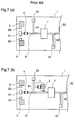
- Figure 7(a) is a plan view illustrating a prior art monolithic microwave semiconductor integrated circuit device. In the figure,
reference numeral 1 designates a semiconductor substrate comprising GaAs, Si, or the like,numeral 3 designated via-holes,numeral 4 designates a capacitor comprising a lamination of metal/insulator/metal (hereinafter referred to as MIM capacitor),numeral 7 designates a transistor, such as a field effect transistor,numeral 21 designates an input electrode pad,numeral 22 designates ground electrode pads,numeral 23 designates a gate bias electrode pad,numeral 24 designates a drain bias electrode pad,numerals numeral 61 designates a gate side bias line, andnumeral 62 designates a drain side bias line. - In this integrated circuit device, a microwave signal applied to the
input electrode pad 21 is transmitted through theMIM capacitor 4 and thesignal transmission line 51 to the gate of thetransistor 7. An output signal from the drain of thetransistor 7 is transmitted through thesignal transmission line 52 to a subsequent stage circuit (not shown). On the other hand, a gate bias voltage applied to the gatebias electrode pad 23 is transmitted through the gateside bias line 61 and thesignal transmission line 51 to the gate of thetransistor 7, and a drain bias voltage applied to the drainbias electrode pad 24 is transmitted through the drainside bias line 62 and thesignal transmission line 52 to the drain of thetransistor 7. The via-holes 3 connect theground electrode pads 22 to a metal layer (not shown) on the rear surface of thesemiconductor substrate 1. TheMIM capacitor 4 connected between theinput electrode pad 21 and the gate of thetransistor 7 is permeable to microwave signals and impermeable to DC signals. - The above-described prior art semiconductor IC has a problem that the transistor easily oscillates at the application of the gate and drain bias voltages. In order to prevent this unwanted oscillation, as shown in figure 7(b), an
oscillation preventing circuit 11 including anMIM capacitor 41 connected to thebias line 61 is included in the IC device. However, since a plurality oftransistors 7 are simultaneously fabricated and the oscillation characteristics of individual transistors are varied due to variations in their transistor characteristics in the fabricating process, in order to prevent the unwanted oscillation of eachtransistor 7, it is necessary for theMIM capacitors 41 of theoscillation preventing circuits 11 corresponding to therespective transistors 7 to have different capacitances according to the different oscillation characteristics of thetransistors 7. However, since theoscillation preventing circuits 11 are fabricated simultaneously with thetransistors 7 and thebias lines 61, it is impossible to change the capacitances of theMIM capacitors 41 after the fabrication of the transistors and the bias lines and the evaluation of the oscillation characteristics of the transistors. Therefore, it is impossible to prevent the unwanted oscillations of all transistors by theoscillation preventing circuits 11. - Further, since the
oscillation preventing circuit 11 comprises theMIM capacitor 41 disposed on a region of the semiconductor substrate and a wiring connecting thecapacitor 41 to thebias line 61 as shown in figure 7(b), the chip area of the IC device is unfavorably increased by the area of theoscillation preventing circuit 11. - It is an object of the present invention to provide an IC device that easily controls oscillation of a transistor and a method of fabricating the IC device.
- Other objects and advantages of the invention will become apparent from the detailed description that follows. The detailed description and specific embodiments described are provided only for illustration since various additions and modifications within the scope of the invention will be apparent to those of skill in the art from the detailed description.
- According to a first aspect of the present invention, an integrated circuit device comprises a substrate; circuit elements including an active element and a bias line for applying a DC bias voltage to the active element, disposed on the substrate; a thermoplastic material layer disposed on a region of the substrate; and a magnetic substance layer disposed on a region of the substrate including a required region on the bias line, and adhered to and supported by the thermoplastic material layer. In this structure, the magnetic substance layer can be formed in an appropriate shape and at an appropriate position on the bias line according to the oscillation characteristics of the active element, such as a transistor, and the magnetic substance layer absorbs the frequency components of the oscillation of the active element, whereby the oscillation of the active element is easily prevented. Further, since the magnetic substance layer is disposed on the bias line, the unwanted increase in the chip area of the integrated circuit device due to the use of the prior art oscillation preventing circuit is avoided.
- According to a second aspect of the present invention, in the above-described integrated circuit device, the thermoplastic material layer is disposed on two regions of the substrate which are opposed each other with the bias line between them, and the magnetic substance layer is disposed across the bias line and adhered to and supported by the thermoplastic material layer. Therefore, as described above, the oscillation of the active element is easily prevented. Further, the unwanted increase in the chip area of the integrated circuit device due to the use of the prior art oscillation preventing circuit is avoided.
- According to a third aspect of the present invention, in the above-described integrated circuit device, the thermoplastic material layer is disposed on a region of the substrate including a required region on the bias line. Therefore, as described above, the oscillation of the active element is easily prevented. Further, the unwanted increase in the chip area of the integrated circuit device due to the use of the prior art oscillation preventing circuit is avoided.
- According to a fourth aspect of the present invention, in the above-described integrated circuit device, the thermoplastic material layer comprises a plurality of island portions which are disposed on opposed two regions of the substrate sandwiching the bias line, and the magnetic substance layer is disposed across the bias line and adhered to and supported by the island portions of the thermoplastic material layer. Therefore, as described above, the oscillation of the active element is easily prevented. Further, the unwanted increase in the chip area of the integrated circuit device due to the use of the prior art oscillation preventing circuit is avoided.
- According to a fifth aspect of the present invention, a method of fabricating an integrated semiconductor device comprises fabricating circuit elements including an active element and a bias line for applying a DC bias voltage to the active element on a substrate; forming a thermoplastic material layer on a region of the substrate; and forming a magnetic substance layer on a region of the substrate including a required region on the bias line by applying a magnetic substance to the thermoplastic material layer and heating the magnetic substance and the thermoplastic material layer to adhere the magnetic substance to the thermoplastic material layer. Since the magnetic substance layer absorbs the frequency components of the oscillation of the active element, the oscillation of the active element is prevented. Further, since the magnetic substance layer is formed on the bias line, the unwanted increase in the chip area of the integrated circuit device due to the use of the prior art oscillation preventing circuit is avoided.
- According to a sixth aspect of the present invention, in the above-described method, after the fabrication of the circuit elements, the oscillation characteristics of the active element is evaluated by applying a DC bias voltage to the active element, and after the evaluation of the oscillation characteristics, the magnetic substance layer is formed in an appropriate shape and on an appropriate position according to the oscillation characteristics of the active element. Therefore, the oscillation of the active element is easily prevented. Further, since the magnetic substance layer is formed on the bias line, the unwanted increase in the chip area of the integrated circuit device due to the use of the prior art oscillation preventing circuit is avoided.
- According to a seventh aspect of the present invention, in the above-described method, the thermoplastic material layer is formed on two regions of the substrate which are opposed each other with the bias line between them, and the magnetic substance layer is formed across the bias line by applying a magnetic substance to the thermoplastic material layer and heating the magnetic substance and the thermoplastic material layer to adhere the magnetic substance to the thermoplastic material layer. Therefore, after evaluating the oscillation characteristics of the active element, the magnetic substance layer can be formed in an appropriate shape and at an appropriate position on the bias line so that the oscillation of the active element is stopped. Further, the unwanted increase in the chip area of the integrated circuit device due to the use of the prior art oscillation preventing circuit is avoided.
- According to an eighth aspect of the present invention, in the above-described method, the thermoplastic material layer is formed on a region of the substrate including a required region on the bias line. Therefore, after evaluating the oscillation characteristics of the active element, the magnetic substance layer can be formed in an appropriate shape and at an appropriate position on the bias line so that the oscillation of the active element is stopped. Further, the unwanted increase in the chip area of the integrated circuit device due to the use of the prior art oscillation preventing circuit is avoided.
- According to a ninth aspect of the present invention, a plurality of island patterns of thermoplastic material are formed on two regions of the substrate which are opposed each other with the bias line between them, and the magnetic substance layer is formed across the bias line by applying a magnetic substance to the island patterns of thermoplastic material and heating the magnetic substance and the island patterns to adhere the magnetic substance to the island patterns. Therefore, after evaluating the oscillation characteristics of the active element, the magnetic substance layer can be formed in an appropriate shape and at an appropriate position on the bias line so that the oscillation of the active element is stopped. Further, the unwanted increase in the chip area of the integrated circuit device due to the use of the prior art oscillation preventing circuit is avoided.
- Figure 1 is a plan view illustrating a semiconductor IC device in accordance with a first embodiment of the present invention.
- Figure 2 is a plan view illustrating a process steps in a method of fabricating the semiconductor IC device in accordance with the first embodiment of the present invention.
- Figure 3 is a plan view illustrating a semiconductor IC device in accordance with a second embodiment of the present invention.
- Figure 4 is a plan view illustrating a process step in a method of fabricating the semiconductor IC device in accordance with the second embodiment of the present invention.
- Figure 5 is a plan view illustrating a semiconductor IC device in accordance with a third embodiment of the present invention.
- Figure 6 is a plan view illustrating a process step in a method of fabricating the semiconductor IC device in accordance with the third embodiment of the present invention.
- Figures 7(a) and 7(b) are plan views illustrating a semiconductor IC device and a semiconductor IC device including an oscillation preventing circuit in accordance with the prior arts.
- Figure 1 is a plan view illustrating a monolithic microwave semiconductor IC device in accordance with a first embodiment of the present invention. In figure 1, the same reference numerals as those in figure 7(a) designate the same or corresponding parts.
Reference numeral 8 designates thermoplastic polyimide layers andreference numeral 9 designates a magnetic substance layer. - In the IC device shown in figure 1, a microwave signal applied to the
input electrode pad 21 is transmitted through theMIM capacitor 4 and thesignal transmission line 51 to the gate of thetransistor 7. An output signal from the drain of thetransistor 7 is transmitted through thesignal transmission line 52 to a subsequent stage circuit (not shown). On the other hand, a gate bias voltage applied to the gatebias electrode pad 23 is transmitted through the gateside bias line 61 and thesignal transmission line 51 to the gate of thetransistor 7, and a drain bias voltage applied to the drainbias electrode pad 24 is transmitted through the drainside bias line 62 and thesignal transmission line 52 to the drain of thetransistor 7. The via-holes 3 connect theground electrode pads 22 to a metal layer (not shown) on the rear surface of thesemiconductor substrate 1. TheMIM capacitor 4 connected between theinput electrode pad 21 and the gate of thetransistor 7 is permeable to microwave signals and impermeable to DC signals. Thethermoplastic polyimide layers 8 are located on both sides of the gateside bias line 61. Themagnetic substance layer 9 is adhered to thethermoplastic polyimide layers 8 across the gateside bias line 61, whereby themagnetic substance 9 is fixed to thesemiconductor substrate 1. Themagnetic substance layer 9 comprises thermoplastic polyimide containing ferrite grains, or ferrite in the shape of a plate or beads. - A description is given of the method for fabricating the IC device shown in figure 1. Figure 2 is a plan view illustrating a process step in the fabricating method. In figure 2, the same reference numerals as in figure 1 designate the same or corresponding parts.
- Initially, the via-
holes 3, theMIM capacitor 4, thetransistor 7, theelectrode pads 21 to 24, thesignal transmission lines semiconductor substrate 1. Thereafter, thethermoplastic polyimide layers 8 are formed on thesemiconductor substrate 1 at the both sides of thebias line 61 as shown in figure 2. Then, DC bias voltage is applied to the gate and the drain of thetransistor 7 to evaluate the oscillation characteristics of thetransistor 7. If thetransistor 7 is oscillating, themagnetic substance 9 which comprises thermoplastic polyimide containing ferrite grains, or ferrite in the shape of a plate or a bead is pressed onto thethermoplastic polyimide layers 8, and they are heated to adhere themagnetic substance 9 to the polyimide layers 8, whereby themagnetic substance 9 is fixed to thesemiconductor substrate 1. In this way, the IC device shown in figure 1 on which themagnetic substance layer 9 for preventing oscillation of thetransistor 7 is disposed across the gateside bias line 61 is fabricated. When it is confirmed in the evaluation of the oscillation characteristics of the transistor that the transistor is not oscillated, it is not necessary to produce themagnetic substance layer 9. - In this first embodiment of the invention, since the frequency components of the oscillation of the
transistor 7 to which the DC bias voltage is applied are absorbed by themagnetic substance layer 9, the oscillation of thetransistor 7 is prevented. Further, after the fabrication of the circuit elements, i.e., thetransistor 7, the bias lines 61 and 62, thesignal transmission lines semiconductor substrate 1, thetransistor 7 is operated to evaluate the oscillation characteristics and, thereafter, themagnetic substance layer 9 is formed across the gateside bias line 61. Therefore, the shape and the position of themagnetic substance layer 9 can be appropriately selected according to the oscillation characteristics of thetransistor 7, so that the oscillation of any transistor can be easily prevented. Furthermore, themagnetic substance layer 9 is disposed on thebias line 61, and thethermoplastic polyimide layers 8 for firing themagnetic substance layer 9 to thesemiconductor substrate 1 are disposed on the minimum regions required for fixing themagnetic substance layer 9 at the both sides of the bias line. Therefore, the undesired increase in the chip area of the IC device due to the use of the prior artoscillation preventing circuit 11 shown in figure 7(b) is avoided. - Although the
magnetic substance layer 9 is disposed on the gateside bias line 61, it may be disposed on the drainside bias line 62 or on both of these bias lines. Alternatively, a plurality of magnetic substance layers may be adhered to the thermoplastic polyimide layers 8. - Figure 3 is a plan view illustrating a monolithic microwave semiconductor IC device in accordance with a second embodiment of the present invention. In figure 3, the same reference numerals as those in figure 1 designate the same or corresponding parts.
- In the IC device shown in figure 3, the microwave signal transmission path and the DC bias voltage application path are the same as those already described in the first embodiment. The
thermoplastic polyimide layer 8 is disposed on the drainside bias line 62, and twomagnetic substance layers 9 comprising thermoplastic polyimide containing ferrite grains, or ferrite in the shape of a plate or a bead are disposed on thethermoplastic polyimide layer 8. Themagnetic substance layers 9 are adhered to thethermoplastic polyimide layer 8, whereby themagnetic substance layers 9 are fixed to thesemiconductor substrate 1. Although in the above-described first embodiment thethermoplastic polyimide layer 8 is not present on the bias line, in this second embodiment it is disposed across the bias line. - A description is given of the method for fabricating the IC device shown in figure 3. Figure 4 is a plan view illustrating a process step in the fabricating method. In figure 4, the same reference numerals as in figure 3 designate the same or corresponding parts.
- Initially, the via-
holes 3, theMIM capacitor 4, thetransistor 7, theelectrode pads 21 to 24, thesignal transmission lines semiconductor substrate 1. Thereafter, thethermoplastic polyimide layer 8 is formed on thesemiconductor substrate 1 across thebias line 62 as shown in figure 4. Then, DC bias voltage is applied to the gate and the drain of thetransistor 7 to evaluate the oscillation characteristics of thetransistor 7. If thetransistor 7 is oscillating, themagnetic substance 9 which comprises thermoplastic polyimide containing ferrite grains, or ferrite in the shape of plates or beads is pressed onto thethermoplastic polyimide layer 8, and they are heated to adhere themagnetic substance 9 to thepolyimide layer 8, whereby themagnetic substance 9 is fixed to thesemiconductor substrate 1. In this way, the IC device shown in figure 3 on which themagnetic substance layers 9 for preventing oscillation of thetransistor 7 are disposed across the drainside bias line 62 is fabricated. When it is confirmed in the evaluation of the oscillation characteristics of the transistor that the transistor is not oscillated, it is not necessary to produce the magnetic substance layers 9. - In this second embodiment of the invention, as in the above-described first embodiment, since the frequency components of the oscillation of the
transistor 7 are absorbed by themagnetic substance layers 9, the oscillation of thetransistor 7 is prevented. Further, since themagnetic substance layers 9 are formed on the drainside bias line 62 after the evaluation of the oscillation characteristics of thetransistor 7, the shape and the position of themagnetic substance layers 9 can be appropriately selected according to the oscillation characteristics of thetransistor 7. Therefore, it is possible to prevent the oscillation of any transistor. Further, themagnetic substance layers 9 are disposed on thebias line 62, and thethermoplastic polyimide layer 8 is disposed on the minimum region, including a region on thebias line 62, required for fixing the magnetic substance layers 9. Therefore, the undesired increase in the chip area of the IC device due to the use of the prior artoscillation preventing circuit 11 shown in figure 7(b) is avoided. - Although the
magnetic substance layer 9 is disposed on the drainside bias line 62, it may be disposed on the gateside bias line 61 or on both of these bias lines. Alternatively, the magnetic substance and the thermoplastic polyimide layer according to this second embodiment may be disposed on one of the bias lines 61 and 62 while the magnetic substance and the thermoplastic polyimide layer according to the above-described first embodiment are disposed on the other bias line. - Although two magnetic substance layers are adhered to the
thermoplastic polyimide layer 8, a single magnetic substance layer or three or more magnetic substance layers may be adhered. - Figure 5 is a plan view illustrating a monolithic microwave semiconductor IC device in accordance with a third embodiment of the present invention. In the figure, the same reference numerals as those in figure 1 designate the same or corresponding parts.
Reference numeral 10 designates island patterns of thermoplastic polyimide (hereinafter referred to as thermoplastic polyimide patterns). - In the IC device shown in figure 5, the microwave signal transmission path and the DC bias voltage application path are the same as those already described in the first embodiment. The
thermoplastic polyimide patterns 10 are disposed on thesemiconductor substrate 1 at the both sides of the gateside bias line 61. Themagnetic substance layer 9 comprising thermoplastic polyimide containing ferrite grains, or ferrite in the shape of a plate or a bead is disposed across thebias line 61 and adhered to thethermoplastic polyimide patterns 10, whereby it is fixed to thesemiconductor substrate 1. While in the above-described first and second embodiments a plate-shaped thermoplastic polyimide layer is employed, in this third embodiment a plurality of island patterns of thermoplastic polyimide are employed. - A description is given of the method for fabricating the IC device shown in figure 5. Figure 6 is a plan view illustrating a process step in the fabricating method. In figure 6, the same reference numerals as in figure 5 designate the same or corresponding parts.
- Initially, the via-
holes 3, theMIM capacitor 4, thetransistor 7, theelectrode pads 21 to 24, thesignal transmission lines semiconductor substrate 1. Thereafter, thethermoplastic polyimide patterns 10 are formed on thesemiconductor substrate 1 at the both sides of thebias line 61 as shown in figure 6. Then, DC bias voltage is applied to the gate and the drain of thetransistor 7 to evaluate the oscillation characteristics of thetransistor 7. If thetransistor 7 is oscillating, themagnetic substance 9 which comprises thermoplastic polyimide containing ferrite grains, or ferrite in the shape of a plate or a bead is pressed onto thethermoplastic polyimide patterns 10, and they are heated to adhere themagnetic substance 9 to thepolyimide patterns 10, whereby themagnetic substance 9 is fixed to thesemiconductor substrate 1. In this way, the IC device shown in figure 5 on which themagnetic substance layer 9 for preventing oscillation of thetransistor 7 is disposed across the drainside bias line 62 is fabricated. When it is confirmed in the evaluation of the oscillation characteristics of the transistor that the transistor is not oscillated, it is not necessary to produce themagnetic substance layer 9. - Also in this third embodiment of the invention, as in the above-described first and second embodiments, since the frequency components of the oscillation of the
transistor 7 are absorbed by themagnetic substance layer 9, the oscillation of thetransistor 7 is prevented. Further, since themagnetic substance layer 9 is formed on the gateside bias line 61 after the evaluation of the oscillation characteristics of thetransistor 7, the shape and the position of themagnetic substance layer 9 can be appropriately selected according to the oscillation characteristics of thetransistor 7. Therefore, it is possible to prevent the oscillation of any transistor. Further, themagnetic substance layer 9 is disposed on thebias line 61, and thethermoplastic polyimide patterns 10 are disposed on the minimum regions required for fixing themagnetic substance layer 9 at the both sides of thebias line 61. Therefore, the undesired increase in the chip area of the IC device due to the use of the prior artoscillation preventing circuit 11 shown in figure 7(b) is avoided. - Although the
magnetic substance layer 9 is disposed on the gateside bias line 61, it may be disposed on the drainside bias line 62 or on both of these bias lines. Alternatively, the magnetic substance and the thermoplastic polyimide patterns according to this embodiment may be disposed on one of the bias lines 61 and 62 while the magnetic substance and the thermoplastic polyimide layer according to the above-described first or second embodiment are disposed on the other bias line. - Although a single magnetic substance layer is adhered to the
thermoplastic polyimide patterns 10, a plurality of magnetic substance layers may be adhered.
Claims (17)
- An integrated circuit device (Fig.1) comprising:a substrate (1);circuit elements including an active element (7) and a bias line (61 or 62) for applying a DC bias voltage to the active element (7), disposed on the substrate (1);a thermoplastic material layer (8) disposed on a region of the substrate (1); anda magnetic substance layer (9) disposed on a region of the substrate (1) including a required region on the bias line (61 or 62), said magnetic substance layer (9) being adhered to and supported by the thermoplastic material layer (8).
- The integrated circuit device of claim 1 (Fig.1) comprising:the thermoplastic material layer (8) being disposed on two regions of the substrate (1) which are opposed each other with the bias line (61 or 62) between them; andthe magnetic substance layer (9) being disposed across the bias line (61 or 62) and adhered to and supported by the thermoplastic material layer (8).
- The integrated circuit device of claim 1 (Fig.3) comprising:
the thermoplastic material layer (8) being disposed on a region of the substrate (1) including a required region on the bias line (61 or 62). - The integrated circuit device of claim 1 (Fig.5) comprising:the thermoplastic material layer comprising a plurality of island portions (10), the island portions (10) being disposed on two regions of the substrate (1) which are opposed each other with the bias line (61 or 62) between them; andthe magnetic substance layer (9) being disposed across the bias line (61 or 62) and adhered to and supported by the island portions (10) of the thermoplastic material layer.
- The integrated circuit device of claim 1 wherein the thermoplastic material layer (8) comprises thermoplastic polyimide.
- The integrated circuit device of claim 1 wherein the magnetic substance layer (9) comprises a thermoplastic material containing ferrite grains.
- The integrated circuit device of claim 1 wherein the magnetic substance layer (9) comprises ferrite.
- The integrated circuit device of claim 1 wherein the integrated circuit device is a monolithic semiconductor integrated circuit device.
- A method of fabricating an integrated semiconductor device (Figs.1 & 2) comprising:fabricating circuit elements including an active element (7) and a bias line (61 or 62) for applying a DC bias voltage to the active element (7) on a substrate (1);forming a thermoplastic material layer (8) on a region of the substrate (1); andforming a magnetic substance layer (9) on a region of the substrate (1) including a required region on the bias line (61 or 62) by applying a magnetic substance (9) to the thermoplastic material layer (8) and heating the magnetic substance (9) and the thermoplastic material layer (8) to adhere the magnetic substance (9) to the thermoplastic material layer (8).
- The method of claim 9 including:after the fabrication of the circuit elements, evaluating the oscillation characteristics of the active element (7) by applying a DC bias voltage to the active element; andafter the evaluation of the oscillation characteristics of the active element, forming the magnetic substance layer (9) in an appropriate shape and on an appropriate position according to the oscillation characteristics of the active element.
- The method of claim 9 (Figs.1 & 2) including:forming the thermoplastic material layer (8) on two regions of the substrate (1) which are opposed each other with the bias line (61 or 62) between them; andforming the magnetic substance layer (9) across the bias line (61 or 62) by applying a magnetic substance (9) to the thermoplastic material layer (8) and heating the magnetic substance (9) and the thermoplastic material layer (8) to adhere the magnetic substance (9) to the thermoplastic material layer (8).
- The method of claim 9 (Figs. 3 & 4) including:
forming the thermoplastic material layer (8) on a region of the substrate (1) including a required region on the bias line (61 or 62). - The method of claim 9 (Figs. 5 & 6) including:forming a plurality of island patterns of thermoplastic material (10) on two regions of the substrate (1) which are opposed each other with the bias line (61 or 62) between them; andforming the magnetic substance layer (9) across the bias line (61 or 62) by applying a magnetic substance (9) to the island patterns of thermoplastic material (10) and heating the magnetic substance (9) and the island patterns (10) to adhere the magnetic substance (9) to the island patterns (10).
- The method of claim 9 wherein the thermoplastic material layer (8) comprises thermoplastic polyimide.
- The method of claim 9 wherein the magnetic substance layer (9) comprises a thermoplastic material containing ferrite grains.
- The method of claim 9 wherein the magnetic substance layer (9) comprises ferrite.
- The method of claim 9 wherein the integrated circuit device is a monolithic semiconductor integrated circuit device.
Priority Applications (1)
| Application Number | Priority Date | Filing Date | Title |
|---|---|---|---|
| EP00117641A EP1059666A1 (en) | 1995-04-05 | 1996-01-17 | Monolithic semiconductor integrated circuit device |
Applications Claiming Priority (3)
| Application Number | Priority Date | Filing Date | Title |
|---|---|---|---|
| JP80221/95 | 1995-04-05 | ||
| JP8022195 | 1995-04-05 | ||
| JP7080221A JPH08279596A (en) | 1995-04-05 | 1995-04-05 | Integrated circuit device and its manufacture |
Related Child Applications (1)
| Application Number | Title | Priority Date | Filing Date |
|---|---|---|---|
| EP00117641.1 Division-Into | 2000-08-16 |
Publications (3)
| Publication Number | Publication Date |
|---|---|
| EP0736902A2 true EP0736902A2 (en) | 1996-10-09 |
| EP0736902A3 EP0736902A3 (en) | 1997-10-29 |
| EP0736902B1 EP0736902B1 (en) | 2001-09-26 |
Family
ID=13712321
Family Applications (2)
| Application Number | Title | Priority Date | Filing Date |
|---|---|---|---|
| EP00117641A Withdrawn EP1059666A1 (en) | 1995-04-05 | 1996-01-17 | Monolithic semiconductor integrated circuit device |
| EP96100652A Expired - Lifetime EP0736902B1 (en) | 1995-04-05 | 1996-01-17 | Integrated circuit device and method for fabricating integrated circuit device |
Family Applications Before (1)
| Application Number | Title | Priority Date | Filing Date |
|---|---|---|---|
| EP00117641A Withdrawn EP1059666A1 (en) | 1995-04-05 | 1996-01-17 | Monolithic semiconductor integrated circuit device |
Country Status (4)
| Country | Link |
|---|---|
| US (1) | US5675184A (en) |
| EP (2) | EP1059666A1 (en) |
| JP (1) | JPH08279596A (en) |
| DE (1) | DE69615437T2 (en) |
Cited By (2)
| Publication number | Priority date | Publication date | Assignee | Title |
|---|---|---|---|---|
| EP0739034A2 (en) * | 1995-04-20 | 1996-10-23 | Mitsubishi Denki Kabushiki Kaisha | Integrated circuit device and fabricating method thereof |
| WO2003054959A3 (en) * | 2001-12-20 | 2004-04-29 | Eupec Gmbh & Co Kg | Circuit arrangement comprising electronic components on a nonconducting supporting substrate |
Families Citing this family (33)
| Publication number | Priority date | Publication date | Assignee | Title |
|---|---|---|---|---|
| JP3185918B2 (en) * | 1996-08-05 | 2001-07-11 | 株式会社村田製作所 | Electronic equipment |
| US6329234B1 (en) | 2000-07-24 | 2001-12-11 | Taiwan Semiconductor Manufactuirng Company | Copper process compatible CMOS metal-insulator-metal capacitor structure and its process flow |
| JP4804643B2 (en) * | 2001-05-08 | 2011-11-02 | 三菱電機株式会社 | High frequency circuit device and manufacturing method thereof |
| US7091542B1 (en) * | 2005-01-28 | 2006-08-15 | International Business Machines Corporation | Method of forming a MIM capacitor for Cu BEOL application |
| US20060197183A1 (en) * | 2005-03-01 | 2006-09-07 | International Business Machines Corporation | Improved mim capacitor structure and process |
| US7223654B2 (en) * | 2005-04-15 | 2007-05-29 | International Business Machines Corporation | MIM capacitor and method of fabricating same |
| US8696662B2 (en) | 2005-05-12 | 2014-04-15 | Aesculap Ag | Electrocautery method and apparatus |
| US9339323B2 (en) | 2005-05-12 | 2016-05-17 | Aesculap Ag | Electrocautery method and apparatus |
| US8728072B2 (en) | 2005-05-12 | 2014-05-20 | Aesculap Ag | Electrocautery method and apparatus |
| US7862565B2 (en) | 2005-05-12 | 2011-01-04 | Aragon Surgical, Inc. | Method for tissue cauterization |
| US8574229B2 (en) | 2006-05-02 | 2013-11-05 | Aesculap Ag | Surgical tool |
| JP5078471B2 (en) * | 2007-07-06 | 2012-11-21 | 三菱電機株式会社 | High frequency amplifier |
| US8870867B2 (en) | 2008-02-06 | 2014-10-28 | Aesculap Ag | Articulable electrosurgical instrument with a stabilizable articulation actuator |
| KR101580925B1 (en) * | 2009-04-28 | 2015-12-30 | 삼성전자주식회사 | Chip On Board Type Package |
| BR112012003356B1 (en) | 2010-02-04 | 2021-02-02 | Aesculap Ag | electrosurgical device |
| US8419727B2 (en) | 2010-03-26 | 2013-04-16 | Aesculap Ag | Impedance mediated power delivery for electrosurgery |
| US8827992B2 (en) | 2010-03-26 | 2014-09-09 | Aesculap Ag | Impedance mediated control of power delivery for electrosurgery |
| US9173698B2 (en) | 2010-09-17 | 2015-11-03 | Aesculap Ag | Electrosurgical tissue sealing augmented with a seal-enhancing composition |
| US8405135B2 (en) | 2010-10-05 | 2013-03-26 | International Business Machines Corporation | 3D via capacitor with a floating conductive plate for improved reliability |
| US9339327B2 (en) | 2011-06-28 | 2016-05-17 | Aesculap Ag | Electrosurgical tissue dissecting device |
| KR102174907B1 (en) | 2012-09-26 | 2020-11-05 | 아에스쿨랍 아게 | Apparatus for tissue cutting and sealing |
| US8901711B1 (en) | 2013-08-07 | 2014-12-02 | International Business Machines Corporation | Horizontal metal-insulator-metal capacitor |
| US10090240B2 (en) | 2016-06-03 | 2018-10-02 | Globalfoundries Inc. | Interconnect structure with capacitor element and related methods |
| US9875959B2 (en) | 2016-06-09 | 2018-01-23 | International Business Machines Corporation | Forming a stacked capacitor |
| US10032711B2 (en) | 2016-07-25 | 2018-07-24 | International Business Machines Corporation | Integrating metal-insulator-metal capacitors with air gap process flow |
| US9893144B1 (en) | 2016-08-05 | 2018-02-13 | International Business Machines Corporation | Methods for fabricating metal-insulator-metal capacitors |
| US9698213B1 (en) | 2016-09-28 | 2017-07-04 | International Business Machines Corporation | Vertical MIM capacitor |
| US9876068B1 (en) | 2016-10-31 | 2018-01-23 | International Business Machines Corporation | High-K metal-insulator-metal capacitor and method of manufacturing the same |
| US10008558B1 (en) | 2017-01-05 | 2018-06-26 | International Business Machines Corporation | Advanced metal insulator metal capacitor |
| US10032855B1 (en) | 2017-01-05 | 2018-07-24 | International Business Machines Corporation | Advanced metal insulator metal capacitor |
| US10090378B1 (en) | 2017-03-17 | 2018-10-02 | International Business Machines Corporation | Efficient metal-insulator-metal capacitor |
| US11031457B2 (en) | 2017-12-15 | 2021-06-08 | International Business Machines Corporation | Low resistance high capacitance density MIM capacitor |
| US10497519B1 (en) | 2018-09-27 | 2019-12-03 | International Business Machines Corporation | Back-end-of-the line capacitor |
Citations (6)
| Publication number | Priority date | Publication date | Assignee | Title |
|---|---|---|---|---|
| JPS5797201A (en) * | 1980-12-09 | 1982-06-16 | Fujitsu Ltd | Integrated circuit for microwave |
| EP0169694A2 (en) * | 1984-07-25 | 1986-01-29 | Rca Licensing Corporation | Component providing high frequency signal suppression |
| US4716389A (en) * | 1986-10-20 | 1987-12-29 | Honeywell Inc. | Millimeter wave microstrip surface mounted attenuator |
| JPH0352302A (en) * | 1989-07-19 | 1991-03-06 | Sanyo Electric Co Ltd | Monolithic microwave integrated circuit |
| EP0461316A1 (en) * | 1989-03-28 | 1991-12-18 | General Electric Company | Die attachment |
| JPH05235655A (en) * | 1992-02-19 | 1993-09-10 | Toshiba Lighting & Technol Corp | Amplifier circuit for high frequency |
Family Cites Families (4)
| Publication number | Priority date | Publication date | Assignee | Title |
|---|---|---|---|---|
| US3959874A (en) * | 1974-12-20 | 1976-06-01 | Western Electric Company, Inc. | Method of forming an integrated circuit assembly |
| US5138431A (en) * | 1990-01-31 | 1992-08-11 | Vlsi Technology, Inc. | Lead and socket structures with reduced self-inductance |
| US5469334A (en) * | 1991-09-09 | 1995-11-21 | Power Integrations, Inc. | Plastic quad-packaged switched-mode integrated circuit with integrated transformer windings and mouldings for transformer core pieces |
| JP3137223B2 (en) * | 1995-01-20 | 2001-02-19 | 三菱電機株式会社 | High frequency amplifier and its oscillation prevention method |
-
1995
- 1995-04-05 JP JP7080221A patent/JPH08279596A/en active Pending
-
1996
- 1996-01-17 DE DE69615437T patent/DE69615437T2/en not_active Expired - Fee Related
- 1996-01-17 US US08/587,527 patent/US5675184A/en not_active Expired - Fee Related
- 1996-01-17 EP EP00117641A patent/EP1059666A1/en not_active Withdrawn
- 1996-01-17 EP EP96100652A patent/EP0736902B1/en not_active Expired - Lifetime
Patent Citations (6)
| Publication number | Priority date | Publication date | Assignee | Title |
|---|---|---|---|---|
| JPS5797201A (en) * | 1980-12-09 | 1982-06-16 | Fujitsu Ltd | Integrated circuit for microwave |
| EP0169694A2 (en) * | 1984-07-25 | 1986-01-29 | Rca Licensing Corporation | Component providing high frequency signal suppression |
| US4716389A (en) * | 1986-10-20 | 1987-12-29 | Honeywell Inc. | Millimeter wave microstrip surface mounted attenuator |
| EP0461316A1 (en) * | 1989-03-28 | 1991-12-18 | General Electric Company | Die attachment |
| JPH0352302A (en) * | 1989-07-19 | 1991-03-06 | Sanyo Electric Co Ltd | Monolithic microwave integrated circuit |
| JPH05235655A (en) * | 1992-02-19 | 1993-09-10 | Toshiba Lighting & Technol Corp | Amplifier circuit for high frequency |
Non-Patent Citations (3)
| Title |
|---|
| PATENT ABSTRACTS OF JAPAN vol. 006, no. 182 (E-131), 18 September 1982 & JP 57 097201 A (FUJITSU LTD), 16 June 1982, * |
| PATENT ABSTRACTS OF JAPAN vol. 015, no. 195 (E-1069), 20 May 1991 & JP 03 052302 A (SANYO ELECTRIC CO LTD), 6 March 1991, * |
| PATENT ABSTRACTS OF JAPAN vol. 017, no. 691 (E-1479), 17 December 1993 & JP 05 235655 A (TOSHIBA LIGHTING & TECHNOL CORP), 10 September 1993, * |
Cited By (3)
| Publication number | Priority date | Publication date | Assignee | Title |
|---|---|---|---|---|
| EP0739034A2 (en) * | 1995-04-20 | 1996-10-23 | Mitsubishi Denki Kabushiki Kaisha | Integrated circuit device and fabricating method thereof |
| EP0739034A3 (en) * | 1995-04-20 | 1999-07-14 | Mitsubishi Denki Kabushiki Kaisha | Integrated circuit device and fabricating method thereof |
| WO2003054959A3 (en) * | 2001-12-20 | 2004-04-29 | Eupec Gmbh & Co Kg | Circuit arrangement comprising electronic components on a nonconducting supporting substrate |
Also Published As
| Publication number | Publication date |
|---|---|
| JPH08279596A (en) | 1996-10-22 |
| EP1059666A1 (en) | 2000-12-13 |
| EP0736902B1 (en) | 2001-09-26 |
| DE69615437D1 (en) | 2001-10-31 |
| EP0736902A3 (en) | 1997-10-29 |
| DE69615437T2 (en) | 2002-07-11 |
| US5675184A (en) | 1997-10-07 |
Similar Documents
| Publication | Publication Date | Title |
|---|---|---|
| US5675184A (en) | Integrated circuit device | |
| US5635762A (en) | Flip chip semiconductor device with dual purpose metallized ground conductor | |
| US7323770B2 (en) | Hybrid integrated circuit device, and method for fabricating the same, and electronic device | |
| GB2269935A (en) | Compact semiconductor device with moulded body | |
| EP0818823A2 (en) | Radio frequency module and method for fabricating the radio frequency module | |
| JPH045289B2 (en) | ||
| US6661101B2 (en) | Semiconductor device | |
| US6710426B2 (en) | Semiconductor device and transceiver apparatus | |
| JP3328542B2 (en) | High frequency semiconductor integrated circuit device | |
| JP2001044448A (en) | Field-effect transistor, monolithic microwave integrated circuit including the field-effect transistor and design method | |
| JPH06252208A (en) | Semiconductor integrated circuit device | |
| JPH02288409A (en) | Resistance feedback type amplifier | |
| JPH01173761A (en) | High-frequency transistor | |
| US5786627A (en) | Integrated circuit device and fabricating thereof | |
| JPS6348855A (en) | Monolithick microwave integrated circuit | |
| JPH04113653A (en) | Semiconductor device | |
| JPH02241046A (en) | Manufacture of semiconductor integrated circuit | |
| JPH10126032A (en) | Structure and method for mounting surface mounting parts | |
| JP2802375B2 (en) | Frequency characteristic expansion method for mixed circuit of electric and optical elements | |
| JPH04261206A (en) | Amplifier | |
| JP2674546B2 (en) | Beam-lead type semiconductor device manufacturing method | |
| JPH03145141A (en) | Semiconductor device | |
| JPH0786612A (en) | Monolithic semiconductor device | |
| JPS63133701A (en) | Microwave semiconductor device | |
| JPH05211279A (en) | Hybrid integrated circuit |
Legal Events
| Date | Code | Title | Description |
|---|---|---|---|
| PUAI | Public reference made under article 153(3) epc to a published international application that has entered the european phase |
Free format text: ORIGINAL CODE: 0009012 |
|
| AK | Designated contracting states |
Kind code of ref document: A2 Designated state(s): DE FR GB |
|
| PUAL | Search report despatched |
Free format text: ORIGINAL CODE: 0009013 |
|
| AK | Designated contracting states |
Kind code of ref document: A3 Designated state(s): DE FR GB |
|
| 17P | Request for examination filed |
Effective date: 19971211 |
|
| 17Q | First examination report despatched |
Effective date: 19980923 |
|
| GRAG | Despatch of communication of intention to grant |
Free format text: ORIGINAL CODE: EPIDOS AGRA |
|
| GRAG | Despatch of communication of intention to grant |
Free format text: ORIGINAL CODE: EPIDOS AGRA |
|
| GRAH | Despatch of communication of intention to grant a patent |
Free format text: ORIGINAL CODE: EPIDOS IGRA |
|
| GRAH | Despatch of communication of intention to grant a patent |
Free format text: ORIGINAL CODE: EPIDOS IGRA |
|
| GRAA | (expected) grant |
Free format text: ORIGINAL CODE: 0009210 |
|
| AK | Designated contracting states |
Kind code of ref document: B1 Designated state(s): DE FR GB |
|
| REF | Corresponds to: |
Ref document number: 69615437 Country of ref document: DE Date of ref document: 20011031 |
|
| REG | Reference to a national code |
Ref country code: GB Ref legal event code: IF02 |
|
| REG | Reference to a national code |
Ref country code: GB Ref legal event code: 727 |
|
| REG | Reference to a national code |
Ref country code: GB Ref legal event code: 727A |
|
| ET | Fr: translation filed | ||
| REG | Reference to a national code |
Ref country code: GB Ref legal event code: 727B |
|
| PLBE | No opposition filed within time limit |
Free format text: ORIGINAL CODE: 0009261 |
|
| STAA | Information on the status of an ep patent application or granted ep patent |
Free format text: STATUS: NO OPPOSITION FILED WITHIN TIME LIMIT |
|
| 26N | No opposition filed | ||
| PGFP | Annual fee paid to national office [announced via postgrant information from national office to epo] |
Ref country code: FR Payment date: 20060110 Year of fee payment: 11 |
|
| PGFP | Annual fee paid to national office [announced via postgrant information from national office to epo] |
Ref country code: GB Payment date: 20060111 Year of fee payment: 11 |
|
| PGFP | Annual fee paid to national office [announced via postgrant information from national office to epo] |
Ref country code: DE Payment date: 20060112 Year of fee payment: 11 |
|
| PG25 | Lapsed in a contracting state [announced via postgrant information from national office to epo] |
Ref country code: DE Free format text: LAPSE BECAUSE OF NON-PAYMENT OF DUE FEES Effective date: 20070801 |
|
| GBPC | Gb: european patent ceased through non-payment of renewal fee |
Effective date: 20070117 |
|
| REG | Reference to a national code |
Ref country code: FR Ref legal event code: ST Effective date: 20070930 |
|
| PG25 | Lapsed in a contracting state [announced via postgrant information from national office to epo] |
Ref country code: GB Free format text: LAPSE BECAUSE OF NON-PAYMENT OF DUE FEES Effective date: 20070117 |
|
| PG25 | Lapsed in a contracting state [announced via postgrant information from national office to epo] |
Ref country code: FR Free format text: LAPSE BECAUSE OF NON-PAYMENT OF DUE FEES Effective date: 20070131 |