EP0720301B1 - Convertisseur numérique analogique à trois niveaux à faible consommation - Google Patents
Convertisseur numérique analogique à trois niveaux à faible consommation Download PDFInfo
- Publication number
- EP0720301B1 EP0720301B1 EP95308955A EP95308955A EP0720301B1 EP 0720301 B1 EP0720301 B1 EP 0720301B1 EP 95308955 A EP95308955 A EP 95308955A EP 95308955 A EP95308955 A EP 95308955A EP 0720301 B1 EP0720301 B1 EP 0720301B1
- Authority
- EP
- European Patent Office
- Prior art keywords
- switches
- level
- load
- signals
- generating
- Prior art date
- Legal status (The legal status is an assumption and is not a legal conclusion. Google has not performed a legal analysis and makes no representation as to the accuracy of the status listed.)
- Expired - Lifetime
Links
Images
Classifications
-
- H—ELECTRICITY
- H03—ELECTRONIC CIRCUITRY
- H03M—CODING; DECODING; CODE CONVERSION IN GENERAL
- H03M3/00—Conversion of analogue values to or from differential modulation
- H03M3/02—Delta modulation, i.e. one-bit differential modulation
-
- H—ELECTRICITY
- H03—ELECTRONIC CIRCUITRY
- H03M—CODING; DECODING; CODE CONVERSION IN GENERAL
- H03M3/00—Conversion of analogue values to or from differential modulation
- H03M3/30—Delta-sigma modulation
- H03M3/50—Digital/analogue converters using delta-sigma modulation as an intermediate step
- H03M3/502—Details of the final digital/analogue conversion following the digital delta-sigma modulation
-
- H—ELECTRICITY
- H03—ELECTRONIC CIRCUITRY
- H03M—CODING; DECODING; CODE CONVERSION IN GENERAL
- H03M3/00—Conversion of analogue values to or from differential modulation
- H03M3/30—Delta-sigma modulation
- H03M3/39—Structural details of delta-sigma modulators, e.g. incremental delta-sigma modulators
- H03M3/412—Structural details of delta-sigma modulators, e.g. incremental delta-sigma modulators characterised by the number of quantisers and their type and resolution
- H03M3/422—Structural details of delta-sigma modulators, e.g. incremental delta-sigma modulators characterised by the number of quantisers and their type and resolution having one quantiser only
- H03M3/424—Structural details of delta-sigma modulators, e.g. incremental delta-sigma modulators characterised by the number of quantisers and their type and resolution having one quantiser only the quantiser being a multiple bit one
-
- H—ELECTRICITY
- H03—ELECTRONIC CIRCUITRY
- H03M—CODING; DECODING; CODE CONVERSION IN GENERAL
- H03M3/00—Conversion of analogue values to or from differential modulation
- H03M3/30—Delta-sigma modulation
- H03M3/39—Structural details of delta-sigma modulators, e.g. incremental delta-sigma modulators
- H03M3/436—Structural details of delta-sigma modulators, e.g. incremental delta-sigma modulators characterised by the order of the loop filter, e.g. error feedback type
- H03M3/438—Structural details of delta-sigma modulators, e.g. incremental delta-sigma modulators characterised by the order of the loop filter, e.g. error feedback type the modulator having a higher order loop filter in the feedforward path
- H03M3/454—Structural details of delta-sigma modulators, e.g. incremental delta-sigma modulators characterised by the order of the loop filter, e.g. error feedback type the modulator having a higher order loop filter in the feedforward path with distributed feedback, i.e. with feedback paths from the quantiser output to more than one filter stage
Definitions
- This invention relates generally to three-level digital-to-analog converters and to methods of converting digital signals to analog signals.
- D/A converter converts a digital signal to an analog signal by assigning a voltage weight to each bit in the digital word and summing up the voltage weights of the entire word.
- the D/A converter requires a network of relatively precise components, usually resistors or capacitors.
- the current practice in the design of a D/A converter commonly incorporates a two-level sigma-delta modulator, pulse-width modulator or other similar control devices.
- the sigma-delta modulator employs the technique of oversampling and one-bit quantization.
- the sigma-delta modulator generally has a quantizer and a feedback loop.
- the sigma-delta modulator in a D/A converter receives a digital signal and the quantizer generates output for both the feedback loop and switching circuitry of a load.
- the feedback control by taking the difference between this output and input provides an error signal. By repeating this process, the feedback control forces this error toward zero.
- the output switching circuitry generates an analog signal.
- the sigma-delta modulator requires fewer number of precision circuits than a conventional D/A converter, and is used for a simpler and more efficient D/A converter design.
- the pulse-width modulator converts a digital input code to generate a train of pulse of fixed frequency, with width proportional to the input count.
- the pulse-width modulator typically comprises a counter, comparator and high-frequency clock.
- the pulse-width modulator generates an analog output voltage proportional to the digital input code. This type of D/A conversion is more commonly used when the load is slowly responding system such as a switching regulator, mechanical taped speed servo or electromagnetic controller.
- Two-level control devices as mentioned above alternate between the two outputs, High and Low levels, regardless of how small the digital input is. For instance, if the accumulated error is even slightly positive, the control signals for the High level will result. If the accumulated error is even slightly negative, then the control signals for the Low level will result.
- a two-level D/A converter is disclosed in U.S. Patent No. 5,160,896 to McCorkle.
- the switching circuitry disclosed therein is a class D amplifier including a pair of output MOSFET switches.
- an active device is used as an on-off switch and output variation is controlled by a modulator or supply voltage source.
- the output of a class D amplifier circuit therefore, is derived by switches and there is no gradual translation between different levels.
- the output voltage alternates between positive and negative levels.
- the two-level D/A converter constantly charges its load by either positive or negative voltages and requires an uninterrupted power supply. Such requirements cause constant power consumption and thus inefficient use of power. This can be a serious burden especially for portable voice or audioband products, the appeal of which often depends on a cost effective and compact power supply or a long-lasting battery.
- U.S. Patent No. 5,206,648 to Yukuwa discloses a three-level D/A converter which comprises switches and capacitors between these switches. In such a configuration, the load always draws power from the voltage source regardless of the level of the control signals.
- a three-level D/A converter disclosed in U.S. Patent No. 5,274,375 to Thompson also includes switching capacitors which constantly draw current from the source.
- the Thompson switching capacitor requires two separate voltage sources providing the same voltages with opposite polarities. This is a difficult requirement to meet and often causes distortion in output unless a significant effort is given for calibration of a voltage supply.
- EP-A-0543224 is directed to a speaker driving device including a pair of voice coils which are wound around a driving section of a speaker to generate a bidirectional driving force at the driving section when a current flows through the voice coils in opposite directions.
- the device further includes a constant voltage source for generating a constant voltage, a ⁇ modulating means for producing a one-bit binary digital audio signal by high speed sampling ⁇ -modulation, and first switching means for alternatively applying the constant voltage to a first voice coil or a second voice coil of the pair of voice coils based on the one-bit digital audio signal so as to cause the current to flow through the first and second voice coils in opposite directions.
- Apparatus embodying the present invention provides an improved D/A converter which avoids the above noted disadvantages.
- a digital-to-analog (D/A) converter embodying the present invention is a three-level converter with a class D amplifier.
- the converter comprises a control device, a switching mechanism, and a load.
- the control device converts incoming digital signals to control signals having three levels.
- the switching mechanism coupled with the control device operate in response to the control signals.
- the load coupled with the switches generates analog signals in response to the switches.
- the control device comprises a control loop and a quantizer for generating control signals having three levels, High, Medium and Low.
- the class D amplifier preferably includes four switches which are connected to a power source. The four switches are also connected to the control device to switch in a prearranged configuration in response to the control signals. For example, the first and second switches may close in response to the High level; all four switches may open in response to the Medium level; and the third and fourth switches may close in response to the Low level.
- the load generates an analog signal in positive, zero or negative voltage references in response to the above switch closures.
- a three-level converter embodying the present invention provides D/A conversion with significant power savings over a two level converter by using a third level in which no power is drawn from the source.
- the three-levels may be generated by various devices including a sigma-delta modulator and a pulse-width modulator.
- the third level (called the Medium level in the present invention) causes the switches connecting the source and the load to open. Thus, there is no power drain during the third level.
- the converter is configured to operate at the third level most frequently to further reduce power consumption.
- a control means 1 is designed to receive multi-bit digital signals.
- the control means 1 converts these multi-bit digital signals to control signals that can indicate three levels, herein denoted High, Medium and Low.
- a switch means 2 is coupled with the control means 1 to receive those control signals.
- the switch means 2 then generates positive, zero or negative voltage references in the analog signals in response to the High, Medium or Low levels. The continuous and repeated process of generating these voltage references produces analog signals.
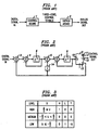
- FIG. 2 illustrates a prior art three-level sigma-delta modulator. Unlike a two level sigma-delta modulator used in a D/A converter, the three-level sigma-delta modulator produces control signals for an additional level (called a Medium level in the present invention), if the accumulated error is near zero.
- a Medium level in the present invention
- a digital signal enters the sigma-delta modulator through a summing junction 3.
- the difference between the digital signal input and a feedback signal from the feedback output section 13 is taken in order to minimize error.
- the output of the summing junction 3 is fed to a summing junction 4.
- This input is summed with the output from the first delay element 5.
- the output of the summing junction 4 is fed to the first delay element 5, in order to accumulate the total error and, through the feedback, to cause the average output value to track the input values gradually.
- the time-average of the analog output is approximately equal to the time-average of the digital input.
- the output of the first delay element 5 is fed to a summing junction 6.
- the input to summing junction 6 is summed with the feedback signal from the feedback output section 13 multiplied by 2 in a multiplier 14.
- the output of the summing junction 6 is fed to a summing junction 7.
- This input is summed with the output from a delay element 8.
- the output of summing junction 7 is fed to the delay element 8.
- the output of the delay element 8 enters a digital signal input section 10 of a quantizer 9.
- the quantizer 9 assigns this input to one of three signal regions and codes these three levels, High, Medium and Low into two binary control signals "H" and "L” at control signal outputs 11 and 12 respectively.
- One-clock cycle delay elements 5 and 8, and the summing junctions 3, 4, 6 and 7 form the forward path of the three-level sigma-delta modulator. Therefore, the sigma-delta modulator converts a sequence of multi-bit digital signals so that a sequence of three-level control signals can represent the input digital signals.
- FIG. 3 illustrates a table that defines the three-level outputs of the quantizer in relationship to the input.
- the symbols, "U”, “H”, “L” and “Y”, denote the incoming or outgoing signals at 10, 11, 12 and 13, respectively.
- the quantity ⁇ is defined as the maximum range of the input digital signal at the digital signal input section 10, that is, - ⁇ ⁇ x ⁇ ⁇ , where x denotes the multi-bit digital input.
- the quantizer receives a multi-bit signal U and codes that input into one of three regions at the signal input section 10. As shown, there is assigned the Medium level for the signal U with a value greater than - ⁇ /2 and less than ⁇ /2. Accordingly, the quantizer now can detect the signal with value near zero to produce the Medium level.
- Such incoming signal U would have produced only the High or Low level in the two-level quantizer.
- the quantizer generates two one-bit control signals H and L that can be set to a logic of high or low and a multi-bit signal Y.
- the control signal H is set to a logic high for the High level when the value of the input signal U falls in the range ⁇ /2 ⁇ U.
- the output Y in this case is set to ⁇ .
- the control signal L is set to a logic high for the Low level when the value of the input signal U falls in the range U ⁇ - ⁇ /2.
- the output Y in this case is set to - ⁇ .
- Both control signals H and L are set to a logic low when the value of the input signal U falls within the range - ⁇ /2 ⁇ U ⁇ - ⁇ /2.
- the multi-bit signal Y with values - ⁇ , 0 or ⁇ is then fed back to summing junctions 3 and 6 to be summed with the input to minimize error.
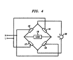
- This switch circuit of the three-level D/A converter comprises a DC voltage source 20 and four switches 15, 16, 17 and 18 are connected to a load 19.
- the switches are generically controlled switching devices such as transistors or relays.
- the load 19 is preferably a two terminal floating load capable of receiving bidirectional current flow, such as a speaker or a transformer.
- the power applied to the load will be V 2 /R when the control signals indicate the High or Low level.
- the control signals indicate the Medium level, no power is applied to the load. This results in a typical power savings of a factor of two or better over a conventional two-level design having only High and Low Levels. Further, in applications such as conversion of digital voice signals, the Medium level is most frequently activated, such as in pauses in a conversation, resulting in further power reduction.
- the D/A converter in this invention can employ any device that can generate control signals having three-levels to improve cost efficiency.
Landscapes
- Engineering & Computer Science (AREA)
- Theoretical Computer Science (AREA)
- Compression, Expansion, Code Conversion, And Decoders (AREA)
- Analogue/Digital Conversion (AREA)
Claims (13)
- Convertisseur numérique/analogique à trois niveaux comportant des moyens de commande à trois niveaux (1) pour convertir les signaux numériques entrants en signaux de commande ayant des niveaux bas, moyen et haut, ledit convertisseur étant caractérisé par :une pluralité de commutateurs (15 à 18) connectés directement auxdits moyens de commande à trois niveaux (1) et réagissant à ceux-ci, chaque paire de commutateurs adjacents de ladite pluralité de commutateurs (15 à 18) étant connectée par un seul noeud ;des moyens de charge (19) positionnés entre ladite pluralité de commutateurs (15 à 18) et réagissant à ceux-ci de façon à générer des signaux analogiques ; etune source de potentiel (20) couplée auxdits commutateurs (15 à 18), sensiblement aucune puissance n'étant extraite de ladite source (20) lorsque lesdits signaux de commande sont audit niveau moyen.
- Convertisseur selon la revendication 1, dans lequel ladite pluralité de commutateurs (15 à 18) comprend des premier, deuxième, troisième et quatrième commutateurs (15 à 18) couplés chacun auxdits moyens de commande à trois niveaux (1) et réagissant à ceux-ci, lesdits premier et deuxième commutateurs (15, 18) se fermant chacun en réponse auxdits signaux de commande pour ledit niveau haut, lesdits troisième et quatrième commutateurs (16, 17) se fermant chacun en réponse auxdits signaux de commande pour ledit niveau bas, et lesdits premier, deuxième, troisième et quatrième commutateurs (15 à 18) s'ouvrant chacun en réponse aux signaux de commande pour ledit niveau moyen.
- Convertisseur selon la revendication 1, dans lequel lesdits moyens de commande (1) comprennent un modulateur sigma-delta à trois niveaux.
- Convertisseur selon la revendication 1, dans lequel lesdits moyens de commande (1) comprennent :des moyens pour recevoir lesdits signaux numériques ;des moyens de commande de rétroaction pour minimiser les erreurs dans lesdits moyens de commande ; etdes moyens pour quantifier lesdits signaux numériques en lesdits signaux de commande ayant trois niveaux, haut, moyen et bas.
- Convertisseur selon la revendication 4, dans lequel lesdits moyens pour la quantification comprennent :une section d'entrée de signal numérique pour recevoir lesdits signaux numériques ;une section de sortie de signal numérique pour générer des signaux numériques pour lesdits moyens de commande de rétroaction ; etune section de sortie de signal de commande pour générer des signaux de commande pour lesdits niveaux haut, moyen et bas.
- Convertisseur selon la revendication 2, dans lequel lesdits moyens de charge (19) sont des moyens de charge à amplificateur de classe D (19) comprenant :des moyens pour générer une référence de tension positive aux bornes desdits moyens de charge (19) lorsque lesdits premier et deuxième commutateurs (15, 18) sont fermés pour activer lesdits moyens de charge (19) ;des moyens pour générer une référence de tension négative aux bornes desdits moyens de charge (19) lorsque lesdits troisième et quatrième commutateurs (16, 17) sont fermés pour activer les moyens de charge (19) ; etdes moyens pour générer une référence de tension nulle aux bornes desdits moyens de charge (19) lorsque lesdits premier, deuxième, troisième et quatrième commutateurs (15 à 18) sont ouverts pour désactiver lesdits moyens de charge (19).
- Convertisseur selon la revendication 1, dans lequel lesdits moyens de charge (19) comprennent un haut-parleur.
- Convertisseur selon la revendication 1, dans lequel lesdits moyens de charge (19) comprennent un transformateur.
- Procédé pour convertir des signaux numériques en signaux analogiques comportant l'étape de conversion des signaux numériques entrants en signaux de commande ayant des niveaux haut, moyen et bas, et caractérisé par les étapes suivantes :l'établissement de l'état d'une pluralité de commutateurs (15 à 18) en réponse directe auxdits signaux de commande, chaque paire de commutateurs adjacents de ladite pluralité de commutateurs (15 à 18) étant connectée par un seul noeud ; etla génération de signaux analogiques à partir d'une charge (19) positionnée entre ladite pluralité de commutateurs (15 à 18) en réponse auxdits commutateurs (15 à 18) et dérivés d'une source de potentiel (20) couplée auxdits commutateurs (15 à 18), sensiblement aucune puissance n'étant extraite de ladite source de potentiel (20) lorsque lesdits signaux de commande sont audit niveau moyen.
- Procédé selon la revendication 9, dans lequel l'étape de conversion comprend :la réception desdits signaux numériques entrants ;la conversion desdits signaux numériques entrants de façon à commander ladite étape de conversion ; etla quantification desdits signaux numériques en lesdits signaux de commande quantifiés.
- Procédé selon la revendication 10, dans lequel l'étape de quantification comprend :la réception desdits signaux numériques ;la génération de signaux numériques de rétroaction pour ladite étape de commande ; etla génération de signaux de commande quantifiés pour lesdits niveaux haut, moyen et bas.
- Procédé selon la revendication 11, dans lequel l'étape d'établissement d'état comprend :la fermeture d'un premier commutateur (15) et d'un deuxième commutateur (18) simultanément en réponse auxdits signaux de commande pour ledit niveau haut ;la fermeture d'un troisième commutateur (16) et d'un quatrième commutateur (17) simultanément en réponse auxdits signaux de commande pour ledit niveau bas ; etl'ouverture desdits premier, deuxième, troisième et quatrième commutateurs (15 à 18) simultanément en réponse aux signaux de commande pour ledit niveau moyen.
- Procédé selon la revendication 11, dans lequel l'étape de génération comprend :la génération d'une référence de tension positive aux bornes de ladite charge (19) lorsque lesdits premier et deuxième commutateurs (15, 18) sont fermés de façon à activer ladite charge (19) ;la génération d'une référence de tension négative aux bornes de ladite charge (19) lorsque lesdits troisième et quatrième commutateurs (16, 17) sont fermés de façon à activer ladite charge (19) ; etla génération d'une référence de tension nulle aux bornes de ladite charge (19) lorsque tous les commutateurs (15 à 18) sont ouverts de façon à désactiver ladite charge (19).
Applications Claiming Priority (2)
| Application Number | Priority Date | Filing Date | Title |
|---|---|---|---|
| US08/365,527 US5608401A (en) | 1994-12-28 | 1994-12-28 | Three-level digital-to-analog converter for low-power consumption |
| US365527 | 1994-12-28 |
Publications (2)
| Publication Number | Publication Date |
|---|---|
| EP0720301A1 EP0720301A1 (fr) | 1996-07-03 |
| EP0720301B1 true EP0720301B1 (fr) | 2001-11-21 |
Family
ID=23439232
Family Applications (1)
| Application Number | Title | Priority Date | Filing Date |
|---|---|---|---|
| EP95308955A Expired - Lifetime EP0720301B1 (fr) | 1994-12-28 | 1995-12-11 | Convertisseur numérique analogique à trois niveaux à faible consommation |
Country Status (6)
| Country | Link |
|---|---|
| US (1) | US5608401A (fr) |
| EP (1) | EP0720301B1 (fr) |
| JP (1) | JPH08242172A (fr) |
| KR (1) | KR100219969B1 (fr) |
| DE (1) | DE69524049T2 (fr) |
| TW (1) | TW401658B (fr) |
Families Citing this family (11)
| Publication number | Priority date | Publication date | Assignee | Title |
|---|---|---|---|---|
| US5874938A (en) | 1996-08-30 | 1999-02-23 | Usar System Inc. | Pointing device with reduced component count |
| DE19722434C1 (de) * | 1997-05-28 | 1998-10-01 | Siemens Ag | Vorrichtung zur Digital-Analog-Wandlung mit hoher Linearität |
| US6147551A (en) * | 1998-01-05 | 2000-11-14 | Motorola, Inc. | Switched capacitor circuit and method for reducing sampling noise |
| US6137429A (en) * | 1999-03-08 | 2000-10-24 | Motorola, Inc. | Circuit and method for attenuating noise in a data converter |
| DE60024052T2 (de) * | 2000-03-31 | 2006-07-27 | Texas Instruments Inc., Dallas | Pulsbreitenmodulation-D/A-Wandler |
| US6621335B2 (en) | 2001-04-18 | 2003-09-16 | Microsemi Corporation | Class D amplifier with passive RC network |
| TWI278186B (en) * | 2005-02-17 | 2007-04-01 | Via Tech Inc | Method and related apparatus for digital/analogue conversion |
| CN100512014C (zh) * | 2005-04-05 | 2009-07-08 | 中兴通讯股份有限公司 | 一种降低模拟数字转换系统工作噪声的电路 |
| TWI337806B (en) * | 2008-10-30 | 2011-02-21 | Ind Tech Res Inst | Sigma delta class d power amplifier and method thereof |
| JP2010130351A (ja) * | 2008-11-27 | 2010-06-10 | Toshiba Corp | 動き補償装置 |
| US8456341B2 (en) * | 2011-06-03 | 2013-06-04 | Texas Instruments Incorporated | Three-level digital-to-analog converter |
Family Cites Families (9)
| Publication number | Priority date | Publication date | Assignee | Title |
|---|---|---|---|---|
| JPH03143027A (ja) * | 1989-10-27 | 1991-06-18 | Fujitsu Ltd | 3値出力形d/a変換器 |
| NL9002212A (nl) * | 1990-10-11 | 1992-05-06 | Philips Nv | Inrichting voor het voeden van een belasting, alsmede een aandrijfsysteem en een geluidsweergavesysteem voorzien van een dergelijke inrichting. |
| JPH04243326A (ja) * | 1991-01-18 | 1992-08-31 | Nec Corp | オーバサンプリングd−a変換器 |
| JP2828543B2 (ja) * | 1991-08-02 | 1998-11-25 | シャープ株式会社 | スピーカ駆動回路 |
| US5347587A (en) * | 1991-11-20 | 1994-09-13 | Sharp Kabushiki Kaisha | Speaker driving device |
| US5160896A (en) * | 1992-02-18 | 1992-11-03 | Harman International Industries, Incorporated | Class D amplifier |
| US5274375A (en) * | 1992-04-17 | 1993-12-28 | Crystal Semiconductor Corporation | Delta-sigma modulator for an analog-to-digital converter with low thermal noise performance |
| US5257026A (en) * | 1992-04-17 | 1993-10-26 | Crystal Semiconductor, Inc. | Method and apparatus for calibrating a multi-bit delta-sigma modular |
| GB9209498D0 (en) * | 1992-05-01 | 1992-06-17 | Univ Waterloo | Multi-bit dac with dynamic element matching |
-
1994
- 1994-12-28 US US08/365,527 patent/US5608401A/en not_active Expired - Lifetime
-
1995
- 1995-03-18 TW TW084102633A patent/TW401658B/zh not_active IP Right Cessation
- 1995-12-11 EP EP95308955A patent/EP0720301B1/fr not_active Expired - Lifetime
- 1995-12-11 DE DE69524049T patent/DE69524049T2/de not_active Expired - Fee Related
- 1995-12-25 JP JP7336273A patent/JPH08242172A/ja not_active Withdrawn
- 1995-12-27 KR KR1019950059648A patent/KR100219969B1/ko not_active IP Right Cessation
Also Published As
| Publication number | Publication date |
|---|---|
| KR960027368A (ko) | 1996-07-22 |
| DE69524049T2 (de) | 2002-07-04 |
| DE69524049D1 (de) | 2002-01-03 |
| TW401658B (en) | 2000-08-11 |
| US5608401A (en) | 1997-03-04 |
| JPH08242172A (ja) | 1996-09-17 |
| EP0720301A1 (fr) | 1996-07-03 |
| KR100219969B1 (ko) | 1999-09-01 |
Similar Documents
| Publication | Publication Date | Title |
|---|---|---|
| US5347587A (en) | Speaker driving device | |
| US6617908B1 (en) | Switched-capacitor circuits with reduced distortion | |
| US5815102A (en) | Delta sigma pwm dac to reduce switching | |
| EP1550221B1 (fr) | Modulateurs delta-sigma avec meilleure performance de bruit | |
| JP4708159B2 (ja) | デジタルアンプ | |
| US6943620B2 (en) | Delta-sigma amplifiers with output stage supply voltage variation compensations and methods and digital amplifier systems using the same | |
| US4920544A (en) | Delta-sigma modulator | |
| US6956514B1 (en) | Delta-sigma modulators with improved noise performance | |
| JP3143567B2 (ja) | デルタシグマ変調器 | |
| EP0720301B1 (fr) | Convertisseur numérique analogique à trois niveaux à faible consommation | |
| EP0084353A2 (fr) | Modulateur delta-sigma réalisé avec des capacités commutées | |
| WO2004059848A2 (fr) | Modulation d'un signal d'entree numerique au moyen d'un modulateur de signal numerique et eclatement du signal | |
| CA2198547A1 (fr) | Bloc d'alimentation a decoupage c.c./c.c.utilisant un convertisseur delta-sigma dans un controleur a boucle fermee. | |
| EP1248374A2 (fr) | Procédé et appareil pour fournir à un modulateur sigma-delta un signal de tremblement dépendant du signal d'entrée | |
| JP2008067181A (ja) | デルタシグマ変調器の制御方法およびデルタシグマ変調器 | |
| JPS6165626A (ja) | A/d変換器 | |
| EP1139571B1 (fr) | Convertisseur N/A à modulation de largeur d'impulsion | |
| US8299866B2 (en) | Method and device including signal processing for pulse width modulation | |
| US6980139B2 (en) | Sigma-delta-modulator | |
| US5206648A (en) | Oversampling da converter with operational amplifier driven by a single reference voltage | |
| JP3009597B2 (ja) | 多ビットδςディジタル/アナログ変換器 | |
| WO1999048205A1 (fr) | Modulateur d'impulsions en largeur double face | |
| JP2000049613A (ja) | ディジタルスイッチングアンプ | |
| US20140368367A1 (en) | Continuous-time sigma-delta modulator and continuous-time sigma-delta modulating method | |
| WO2000070752A1 (fr) | Amplificateur numerique |
Legal Events
| Date | Code | Title | Description |
|---|---|---|---|
| PUAI | Public reference made under article 153(3) epc to a published international application that has entered the european phase |
Free format text: ORIGINAL CODE: 0009012 |
|
| AK | Designated contracting states |
Kind code of ref document: A1 Designated state(s): DE ES FR GB IT NL |
|
| 17P | Request for examination filed |
Effective date: 19961211 |
|
| 17Q | First examination report despatched |
Effective date: 19990917 |
|
| GRAG | Despatch of communication of intention to grant |
Free format text: ORIGINAL CODE: EPIDOS AGRA |
|
| GRAG | Despatch of communication of intention to grant |
Free format text: ORIGINAL CODE: EPIDOS AGRA |
|
| GRAH | Despatch of communication of intention to grant a patent |
Free format text: ORIGINAL CODE: EPIDOS IGRA |
|
| GRAH | Despatch of communication of intention to grant a patent |
Free format text: ORIGINAL CODE: EPIDOS IGRA |
|
| GRAA | (expected) grant |
Free format text: ORIGINAL CODE: 0009210 |
|
| AK | Designated contracting states |
Kind code of ref document: B1 Designated state(s): DE ES FR GB IT NL |
|
| PG25 | Lapsed in a contracting state [announced via postgrant information from national office to epo] |
Ref country code: NL Free format text: LAPSE BECAUSE OF FAILURE TO SUBMIT A TRANSLATION OF THE DESCRIPTION OR TO PAY THE FEE WITHIN THE PRESCRIBED TIME-LIMIT Effective date: 20011121 Ref country code: IT Free format text: LAPSE BECAUSE OF FAILURE TO SUBMIT A TRANSLATION OF THE DESCRIPTION OR TO PAY THE FEE WITHIN THE PRE;WARNING: LAPSES OF ITALIAN PATENTS WITH EFFECTIVE DATE BEFORE 2007 MAY HAVE OCCURRED AT ANY TIME BEFORE 2007. THE CORRECT EFFECTIVE DATE MAY BE DIFFERENT FROM THE ONE RECORDED.SCRIBED TIME-LIMIT Effective date: 20011121 |
|
| REG | Reference to a national code |
Ref country code: GB Ref legal event code: IF02 |
|
| REF | Corresponds to: |
Ref document number: 69524049 Country of ref document: DE Date of ref document: 20020103 |
|
| ET | Fr: translation filed | ||
| PG25 | Lapsed in a contracting state [announced via postgrant information from national office to epo] |
Ref country code: GB Free format text: LAPSE BECAUSE OF NON-PAYMENT OF DUE FEES Effective date: 20020221 |
|
| NLV1 | Nl: lapsed or annulled due to failure to fulfill the requirements of art. 29p and 29m of the patents act | ||
| PG25 | Lapsed in a contracting state [announced via postgrant information from national office to epo] |
Ref country code: ES Free format text: LAPSE BECAUSE OF FAILURE TO SUBMIT A TRANSLATION OF THE DESCRIPTION OR TO PAY THE FEE WITHIN THE PRESCRIBED TIME-LIMIT Effective date: 20020530 |
|
| PG25 | Lapsed in a contracting state [announced via postgrant information from national office to epo] |
Ref country code: DE Free format text: LAPSE BECAUSE OF NON-PAYMENT OF DUE FEES Effective date: 20020702 |
|
| PLBE | No opposition filed within time limit |
Free format text: ORIGINAL CODE: 0009261 |
|
| STAA | Information on the status of an ep patent application or granted ep patent |
Free format text: STATUS: NO OPPOSITION FILED WITHIN TIME LIMIT |
|
| GBPC | Gb: european patent ceased through non-payment of renewal fee |
Effective date: 20020221 |
|
| PG25 | Lapsed in a contracting state [announced via postgrant information from national office to epo] |
Ref country code: FR Free format text: LAPSE BECAUSE OF NON-PAYMENT OF DUE FEES Effective date: 20021031 |
|
| 26N | No opposition filed | ||
| REG | Reference to a national code |
Ref country code: FR Ref legal event code: ST |
|
| PG25 | Lapsed in a contracting state [announced via postgrant information from national office to epo] |
Ref country code: FR Free format text: LAPSE BECAUSE OF NON-PAYMENT OF DUE FEES Effective date: 20011231 |