EP0720235A2 - MOSFET comprenant une tranchée avec une couche à dopage delta pour obtenir une faible résistance à l'état conducteur - Google Patents
MOSFET comprenant une tranchée avec une couche à dopage delta pour obtenir une faible résistance à l'état conducteur Download PDFInfo
- Publication number
- EP0720235A2 EP0720235A2 EP95309535A EP95309535A EP0720235A2 EP 0720235 A2 EP0720235 A2 EP 0720235A2 EP 95309535 A EP95309535 A EP 95309535A EP 95309535 A EP95309535 A EP 95309535A EP 0720235 A2 EP0720235 A2 EP 0720235A2
- Authority
- EP
- European Patent Office
- Prior art keywords
- region
- mosfet
- trench
- layer
- delta
- Prior art date
- Legal status (The legal status is an assumption and is not a legal conclusion. Google has not performed a legal analysis and makes no representation as to the accuracy of the status listed.)
- Ceased
Links
- 239000002019 doping agent Substances 0.000 claims abstract description 60
- 210000000746 body region Anatomy 0.000 claims abstract description 53
- 238000009792 diffusion process Methods 0.000 claims description 44
- 239000000758 substrate Substances 0.000 claims description 28
- 238000000034 method Methods 0.000 claims description 19
- 230000015556 catabolic process Effects 0.000 claims description 13
- 229910052751 metal Inorganic materials 0.000 claims description 7
- 239000002184 metal Substances 0.000 claims description 7
- 150000002500 ions Chemical class 0.000 claims description 4
- 239000004065 semiconductor Substances 0.000 claims description 2
- 239000007943 implant Substances 0.000 claims 20
- 230000003247 decreasing effect Effects 0.000 claims 2
- 238000000151 deposition Methods 0.000 claims 2
- 230000015572 biosynthetic process Effects 0.000 claims 1
- 238000004519 manufacturing process Methods 0.000 claims 1
- 229920002120 photoresistant polymer Polymers 0.000 claims 1
- 230000005684 electric field Effects 0.000 description 8
- 239000000969 carrier Substances 0.000 description 4
- 230000008569 process Effects 0.000 description 4
- 230000007480 spreading Effects 0.000 description 4
- 230000000694 effects Effects 0.000 description 3
- ZOXJGFHDIHLPTG-UHFFFAOYSA-N Boron Chemical compound [B] ZOXJGFHDIHLPTG-UHFFFAOYSA-N 0.000 description 2
- OAICVXFJPJFONN-UHFFFAOYSA-N Phosphorus Chemical compound [P] OAICVXFJPJFONN-UHFFFAOYSA-N 0.000 description 2
- 239000008186 active pharmaceutical agent Substances 0.000 description 2
- 230000002411 adverse Effects 0.000 description 2
- 230000008901 benefit Effects 0.000 description 2
- 229910052796 boron Inorganic materials 0.000 description 2
- 239000005380 borophosphosilicate glass Substances 0.000 description 2
- 230000007423 decrease Effects 0.000 description 2
- 230000006872 improvement Effects 0.000 description 2
- 239000000463 material Substances 0.000 description 2
- 229910052698 phosphorus Inorganic materials 0.000 description 2
- 239000011574 phosphorus Substances 0.000 description 2
- 229910021420 polycrystalline silicon Inorganic materials 0.000 description 2
- 229920005591 polysilicon Polymers 0.000 description 2
- 229910052785 arsenic Inorganic materials 0.000 description 1
- RQNWIZPPADIBDY-UHFFFAOYSA-N arsenic atom Chemical compound [As] RQNWIZPPADIBDY-UHFFFAOYSA-N 0.000 description 1
- 238000005094 computer simulation Methods 0.000 description 1
- 239000004020 conductor Substances 0.000 description 1
- 230000006735 deficit Effects 0.000 description 1
- 230000005669 field effect Effects 0.000 description 1
- 238000002513 implantation Methods 0.000 description 1
- 239000012535 impurity Substances 0.000 description 1
- 230000004048 modification Effects 0.000 description 1
- 238000012986 modification Methods 0.000 description 1
- 238000012856 packing Methods 0.000 description 1
- 230000003071 parasitic effect Effects 0.000 description 1
Images


Classifications
-
- H—ELECTRICITY
- H01—ELECTRIC ELEMENTS
- H01L—SEMICONDUCTOR DEVICES NOT COVERED BY CLASS H10
- H01L29/00—Semiconductor devices specially adapted for rectifying, amplifying, oscillating or switching and having potential barriers; Capacitors or resistors having potential barriers, e.g. a PN-junction depletion layer or carrier concentration layer; Details of semiconductor bodies or of electrodes thereof ; Multistep manufacturing processes therefor
- H01L29/66—Types of semiconductor device ; Multistep manufacturing processes therefor
- H01L29/68—Types of semiconductor device ; Multistep manufacturing processes therefor controllable by only the electric current supplied, or only the electric potential applied, to an electrode which does not carry the current to be rectified, amplified or switched
- H01L29/76—Unipolar devices, e.g. field effect transistors
- H01L29/772—Field effect transistors
- H01L29/78—Field effect transistors with field effect produced by an insulated gate
- H01L29/7801—DMOS transistors, i.e. MISFETs with a channel accommodating body or base region adjoining a drain drift region
- H01L29/7802—Vertical DMOS transistors, i.e. VDMOS transistors
-
- H—ELECTRICITY
- H01—ELECTRIC ELEMENTS
- H01L—SEMICONDUCTOR DEVICES NOT COVERED BY CLASS H10
- H01L29/00—Semiconductor devices specially adapted for rectifying, amplifying, oscillating or switching and having potential barriers; Capacitors or resistors having potential barriers, e.g. a PN-junction depletion layer or carrier concentration layer; Details of semiconductor bodies or of electrodes thereof ; Multistep manufacturing processes therefor
- H01L29/02—Semiconductor bodies ; Multistep manufacturing processes therefor
- H01L29/06—Semiconductor bodies ; Multistep manufacturing processes therefor characterised by their shape; characterised by the shapes, relative sizes, or dispositions of the semiconductor regions ; characterised by the concentration or distribution of impurities within semiconductor regions
- H01L29/10—Semiconductor bodies ; Multistep manufacturing processes therefor characterised by their shape; characterised by the shapes, relative sizes, or dispositions of the semiconductor regions ; characterised by the concentration or distribution of impurities within semiconductor regions with semiconductor regions connected to an electrode not carrying current to be rectified, amplified or switched and such electrode being part of a semiconductor device which comprises three or more electrodes
- H01L29/1095—Body region, i.e. base region, of DMOS transistors or IGBTs
-
- H—ELECTRICITY
- H01—ELECTRIC ELEMENTS
- H01L—SEMICONDUCTOR DEVICES NOT COVERED BY CLASS H10
- H01L29/00—Semiconductor devices specially adapted for rectifying, amplifying, oscillating or switching and having potential barriers; Capacitors or resistors having potential barriers, e.g. a PN-junction depletion layer or carrier concentration layer; Details of semiconductor bodies or of electrodes thereof ; Multistep manufacturing processes therefor
- H01L29/66—Types of semiconductor device ; Multistep manufacturing processes therefor
- H01L29/68—Types of semiconductor device ; Multistep manufacturing processes therefor controllable by only the electric current supplied, or only the electric potential applied, to an electrode which does not carry the current to be rectified, amplified or switched
- H01L29/76—Unipolar devices, e.g. field effect transistors
- H01L29/772—Field effect transistors
- H01L29/78—Field effect transistors with field effect produced by an insulated gate
- H01L29/7801—DMOS transistors, i.e. MISFETs with a channel accommodating body or base region adjoining a drain drift region
- H01L29/7802—Vertical DMOS transistors, i.e. VDMOS transistors
- H01L29/7809—Vertical DMOS transistors, i.e. VDMOS transistors having both source and drain contacts on the same surface, i.e. Up-Drain VDMOS transistors
-
- H—ELECTRICITY
- H01—ELECTRIC ELEMENTS
- H01L—SEMICONDUCTOR DEVICES NOT COVERED BY CLASS H10
- H01L29/00—Semiconductor devices specially adapted for rectifying, amplifying, oscillating or switching and having potential barriers; Capacitors or resistors having potential barriers, e.g. a PN-junction depletion layer or carrier concentration layer; Details of semiconductor bodies or of electrodes thereof ; Multistep manufacturing processes therefor
- H01L29/66—Types of semiconductor device ; Multistep manufacturing processes therefor
- H01L29/68—Types of semiconductor device ; Multistep manufacturing processes therefor controllable by only the electric current supplied, or only the electric potential applied, to an electrode which does not carry the current to be rectified, amplified or switched
- H01L29/76—Unipolar devices, e.g. field effect transistors
- H01L29/772—Field effect transistors
- H01L29/78—Field effect transistors with field effect produced by an insulated gate
- H01L29/7801—DMOS transistors, i.e. MISFETs with a channel accommodating body or base region adjoining a drain drift region
- H01L29/7802—Vertical DMOS transistors, i.e. VDMOS transistors
- H01L29/7813—Vertical DMOS transistors, i.e. VDMOS transistors with trench gate electrode, e.g. UMOS transistors
-
- H—ELECTRICITY
- H01—ELECTRIC ELEMENTS
- H01L—SEMICONDUCTOR DEVICES NOT COVERED BY CLASS H10
- H01L29/00—Semiconductor devices specially adapted for rectifying, amplifying, oscillating or switching and having potential barriers; Capacitors or resistors having potential barriers, e.g. a PN-junction depletion layer or carrier concentration layer; Details of semiconductor bodies or of electrodes thereof ; Multistep manufacturing processes therefor
- H01L29/02—Semiconductor bodies ; Multistep manufacturing processes therefor
- H01L29/06—Semiconductor bodies ; Multistep manufacturing processes therefor characterised by their shape; characterised by the shapes, relative sizes, or dispositions of the semiconductor regions ; characterised by the concentration or distribution of impurities within semiconductor regions
- H01L29/08—Semiconductor bodies ; Multistep manufacturing processes therefor characterised by their shape; characterised by the shapes, relative sizes, or dispositions of the semiconductor regions ; characterised by the concentration or distribution of impurities within semiconductor regions with semiconductor regions connected to an electrode carrying current to be rectified, amplified or switched and such electrode being part of a semiconductor device which comprises three or more electrodes
- H01L29/0843—Source or drain regions of field-effect devices
- H01L29/0847—Source or drain regions of field-effect devices of field-effect transistors with insulated gate
Definitions
- This invention relates to current switching MOSFETs having a gate formed in a trench and in particular to a trench MOSFET having a lower resistance when the device is turned on.
- Power MOSFETs are widely used in numerous applications, including automotive electronics, disk drives and power supplies. Generally, these devices function as switches, and they are used to connect a power supply to a load. It is important that the resistance of the device be as low as possible when the switch is closed. Otherwise, power is wasted and excessive heat may be generated.
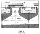
- a common type of power MOSFET currently in use is a planar, double-diffused (DMOS) device, illustrated in the cross-sectional view of Fig. 1.
- An electron current flows laterally from N+ source regions 12 through channel regions formed within P-body regions 14 into an N-epitaxial layer 16.
- Current flow in the channel regions is controlled by a gate 18. After the current leaves the channel regions, it flows downward through N-epitaxial layer 16 into an N+ substrate 20, which forms the drain of the device.
- a parasitic junction field effect transistor (JFET) is formed by the existence of P-body regions 14 on either side of an intervening region of N-epitaxial layer 16.
- a depletion zone 22 adjacent the junction between each of P-body regions 14 and N-epitaxial layer 16 tends to squeeze the current and thereby increase the resistance in this area. As the current proceeds downward through N-epitaxial layer 16 it spreads out and the resistance decreases.
- the gate is formed in a "trench".
- a trench Such a device is illustrated in Fig. 2A, which is a cross-sectional view of a single cell of a MOSFET 100, and in Fig. 2B, which is a plan view of the cell.
- Gates 102 and 104 are formed in trenches and surrounded by gate oxide layers 106 and 108, respectively.
- the trenched gate is often formed in a grid pattern (one section of which is shown in Fig. 2B), the grid representing a single interconnected gate, but a trench gate may also be formed as a series of distinct parallel stripes.
- MOSFET 100 is a double-diffused device which is formed in an N-epitaxial layer 110.
- An N+ source region 112 is formed at the surface of epitaxial layer 110, as is a P+ contact region 114.
- a P-body 116 is located below N+ source region 112 and P+ contact region 114.
- a metal source contact 118 makes contact with the N+ source region 112 and shorts the N+ source region 112 to the P+ contact region 114 and P body 116.
- the N-epitaxial layer 110 is formed on an N+ substrate 120, and a drain contact (not shown) is located at the bottom of the N+ substrate 120.
- the contact for the gates 102 and 104 is likewise not shown, but it is generally made by extending the conductive gate material outside of the trench and forming a metal contact at a location remote from the individual cells.
- the gate is typically made of polysilicon doped with phosphorus or boron.
- a region 111 of N-epitaxial layer 110 between the N+ substrate 120 and the P body 116 is generally more lightly doped with N-type impurities than is N+ substrate 120. This increases the ability of MOSFET 100 to withstand high voltages. Region 111 is sometimes referred to as a "lightly doped” or “drift” region ("drift” referring to the movement of carriers in an electric field). Drift region 111 and N+ substrate 120 constitute the drain of MOSFET 100.
- MOSFET 100 is an N-channel MOSFET.
- a positive voltage is applied to gate 102, a channel region within P-body 116 adjacent the gate oxide 106 becomes inverted and, provided there is a voltage difference between the N+ source region 112 and the N+ substrate 120, an electron current will flow from the source region through the channel region into the drift region 111.
- drift region 111 some of the electron current spreads diagonally at an angle until it hits the N+ substrate 120, and then it flows vertically to the drain. Other portions of the current flow straight down through the drift region 111, and some of the current flows underneath the gate 102 and then downward through the drift region 111.
- the gate 102 is doped with a conductive material. Since MOSFET 100 is an N-channel MOSFET, gate 102 could be polysilicon doped with phosphorus. Gate 102 is insulated from the remainder of MOSFET 100 by the gate oxide 106. The thickness of gate oxide 106 is chosen to set the threshold voltage of MOSFET 100 and may also influence the breakdown voltage of MOSFET 100. The breakdown voltage of a power MOSFET such as MOSFET 100 would typically be no greater than 200 volts and more likely 60 volts or less.
- One feature that makes the trench configuration attractive is that, as described above, the current flows vertically through the channel of the MOSFET. This permits a higher packing density than MOSFETs in which the current flows horizontally through the channel. Greater cell density generally means more MOSFETs per unit area of the substrate and, since the MOSFETs are connected in parallel, the on-resistance of the device is reduced.
- the P+ contact region 114 is quite shallow and does not extend to the lower junction of the P-body region 116. This helps ensure that P-type dopant does not get into the channel region, where it would tend to increase the threshold voltage of the device and cause the turn-on characteristics of the device to vary from one run to another depending on the alignment of the P+ contact region 114.
- the device can withstand only relatively low voltages (e.g., 10 volts) when it is turned off. This is because the depletion spreading around the junction between P-body region 116 and drift region 111 does not adequately protect the corners of the trench (e.g., corner 122 shown in Fig. 1A).
- the MOSFET 100 shown in Fig. 1B is at best a low voltage device.
- Fig. 2C illustrates a modification of MOSFET 100 in which the P+ body contact region 114 is extended downward slightly beyond the lower junction of P-body region 116.
- the higher concentration of P ions in this region increases the size of the depletion area, and this provides some additional shielding around the corner 122 of the trench.
- this device is pushed into breakdown, the generation of carriers will still most likely occur near gate oxide layer 106, and this could lead to the impairment of the gate oxide as described above.
- the breakdown situation was significantly improved in the arrangement shown in Figs. 3A-3C, which was described in U.S. Patent No. 5,072,266 to Bulucea et al.
- MOSFET 300 the P+ region 114 is extended downward below the bottom of the trench to form a deep, heavily-doped P region at the center of the cell. While this provides additional shielding at corner 122, the primary advantage is that carrier generation occurs primarily at the bottom tip 302 of the P+ region 114. This occurs because the electric field is strengthened beneath the tip 302, thereby causing carriers to be generated at that point or along the curvature of the junction rather than adjacent the gate oxide 106. This reduces the stress on gate oxide 106 and improves the reliability of MOSFET 300 under high voltage conditions, even though it may reduce the actual junction breakdown of the device.
- Fig. 3B illustrates a perspective cross-sectional view of the left half of the cell shown in Fig. 3A, as well as portions of the adjoining cells.
- Fig. 3C shows a comparable P-channel device.
- Fig. 3D illustrates how a gate metal 121 may be used to form a connection with gates 102 and 104.
- the deep central P+ region 114 in MOSFET 300 while greatly reducing the adverse consequences of breakdown, also has some unfavorable effects.
- the electron current spreads out when it reaches the drift region 111. This current spreading reduces the average current per unit area in the drift region 111 and therefore reduces the on-resistance of the MOSFET.
- the presence of a deep central P+ region limits this current spreading and increases the on-resistance consistent with high cell densities.
- the trench MOSFET of this invention includes a gate formed in a trench, a source region of a first conductivity type, a body region of a second conductivity type located under the source region, a drain region of first conductivity type located under the body region, and a "lightly doped" or “drift” region within the drain region, the dopant concentration of the drift region being lower than the dopant concentration of the drain region generally.
- the drain may include a substrate or, in "quasi-vertical” embodiments, the drain may include a buried layer of first conductivity type which is connected to the top surface of the semiconductor material via, for example, a "sinker" region.
- the drift region may be formed in an epitaxial layer or in the substrate.
- the delta layer is a layer wherein the concentration of dopant of first conductivity type is greater than the concentration of dopant of first conductivity type in the drift region generally. In many embodiments the delta layer abuts the body region, although in some embodiments the delta layer is separated from the body region.
- the upper boundary of the delta layer is at a level which is above the bottom of the trench in which the gate is formed. In some embodiments, the upper boundary of the delta layer coincides with a lower junction of the body region. The lower boundary of the delta layer may be at a level either above or below the bottom of the trench.
- the MOSFET is typically formed in a cell which is interposed between opposing trenches so as to form a symmetrical structure. In some embodiments, there is a gap between an end of the delta layer and the trench. In some embodiments, a region of second conductivity type extends downward through a central aperture in the delta layer.
- the delta layer may be formed in a MOSFET either with or without a deep central region of second conductivity type.
- the delta layer constitutes a region of relatively low resistivity, as compared to the drift region generally, and therefore operates to spread out the current as it emerges from the lower (drain) end of the channel. This occurs without significant adverse effects on the breakdown characteristics of the MOSFET.
- Fig. 1 illustrates a cross-sectional view of a conventional planar double-diffused MOSFET.
- Figs. 2A and 2B illustrate cross-sectional and plan views, respectively, of a cell of a typical vertical trench N-channel MOSFET having a relatively shallow central P+ contact region.
- Fig. 2C illustrates a cross-sectional view of a similar N-channel MOSFET in which the central P+ contact region has been extended below the bottom edge of the P body region.
- Fig. 3A illustrates a cross-sectional view of a similar N-channel MOSFET in which the central P+ contact region has been extended to a location below the bottom of the trench.
- Fig. 3B illustrates a perspective cross-sectional view of the N-channel MOSFET shown in Fig. 3A.
- Fig. 3C illustrates a perspective cross-sectional view of a similar P-channel MOSFET.
- Fig. 3D illustrates a gate metal contact formed on the top surface of the device.
- Fig. 4 illustrates a cross-sectional view of a MOSFET which includes a deep central P+ region as well as a N delta layer in accordance with this invention.
- Fig. 5 illustrates a graph showing the concentration of dopant at different levels of the MOSFET.
- Fig. 6A illustrates the flow of current in a conventional MOSFET not fabricated in accordance with the principles of this invention.
- Fig. 6B illustrates the flow of current in a MOSFET fabricated in accordance with this invention.
- Figs. 7A, 7B and 7C illustrate the equipotential lines, electric field contour lines and ionization rates, respectively, in a MOSFET fabricated in accordance with this invention.
- Fig. 8 illustrates a cross-sectional view of a MOSFET in which there is a gap between the edges of the delta layer and the walls of the trench.
- Figs. 9A, 9B and 9C illustrate the equipotential lines, electric field contour lines and ionization rates for the MOSFET shown in Fig. 8.
- Fig. 10 illustrates a MOSFET in accordance with this invention in which there is a gap between the edges of the delta layer and a deep diffusion at the center of the cell.
- Figs. 11A-11G illustrate steps in a process of fabricating a MOSFET in accordance with this invention.
- Fig. 12A illustrates an embodiment of a MOSFET with a deep central diffusion and a delta layer which extends below the bottom of the trench but not below the tip of the deep central diffusion.
- Fig. 12B illustrates an embodiment of a MOSFET with a deep central diffusion and a delta layer which extends below the bottom of the trench and the tip of the deep central diffusion.
- Fig. 12C illustrates an embodiment of a MOSFET with a delta layer which underlies the tip of a relatively shallow central diffusion but does not extend below the bottom of the trench.
- Fig. 12D illustrates an embodiment of a MOSFET having a deep central diffusion and a delta layer which does not extend below the bottom of the trench.
- Fig. 12E illustrates an embodiment of a MOSFET without a deep central diffusion and a delta layer which does not extend below the bottom of the trench or to the lower edge of the body region.
- Figs. 13A and 13B illustrate the application of the principles of this invention to "quasi-vertical" MOSFETs, i.e., vertical trench MOSFETs in which the drain contact is made at the top surface of the device.
- MOSFET 400 in accordance with this invention is illustrated in Fig. 4.
- MOSFET 400 generally corresponds to MOSFET 300 shown in Fig. 3A, but in addition a delta layer 402 is located in N-epitaxial layer 110.
- N+ source region 112 would normally be highly doped with a dosage of from 1 x 10 14 to 7 x 10 15 cm -2 .
- P+ contact region 114 could be doped from 1 x 10 14 to 5 x 10 15 cm -2 .
- the doping of P body 116 establishes the threshold voltage.
- P body 116 is normally doped in the range of from 5 x 10 12 to 5 x 10 14 cm -2 .
- the trench in which gate 102 and gate oxide 106 are formed may be rectangular as shown, but it need not be.
- the thickness of the gate oxide 106 would typically be in the range of from 80 ⁇ to 1200 ⁇ .
- N delta layer 402 is doped with N-type dopant to a concentration that is greater than the concentration of N-type dopant in the adjacent portions of drift region 111.
- the dopant concentration of drift region 111 is typically in the range of 5 x 10 14 to 1 x 10 17 cm -3 and the dopant concentration of N+ substrate 120 in the range of 5 x 10 17 to 1 x 10 20 cm -3 .
- Fig. 5 shows a graph which illustrates an example of the dopant concentrations in MOSFET 400.
- the horizontal axis of the graph represents the distance in microns below the surface of the MOSFET, and the vertical axis represents the concentration of dopant in ions-cm -3 .
- the dopant concentration in the N delta layer 402 reaches a maximum at approximately 4 x 10 16 cm -3 and is generally higher than the concentration of N-type dopant in adjacent regions of the drift region 111 which, in this example, remains relatively constant at about 4 x 10 15 cm -3 .
- N delta layer 402 has a lower resistivity than drift region 111 generally, and effectively causes the current to spread out as it leaves the bottom (drain) end of the channel region of MOSFET 400.
- Figs. 6A and 6B illustrate the results of a computer simulation using the two-dimensional device simulator MEDICI.
- the MOSFET was a device having a cell width of 7 microns with a trench approximately 1.5 microns deep.
- the device shown in Fig. 6A is in the form of MOSFET 300 (Fig. 3); the device shown in Fig. 6B is in the form of MOSFET 400 (Fig. 4), which has a delta layer.
- the pattern of lines in Figs. 6A and 6B illustrates the flow of current, the space between each pair of lines representing 5% of the total drain current. It is apparent from Fig. 6B that the current in MOSFET 400 fans out to a much greater degree after it leaves the drain end of the channel than does the current in MOSFET 300. For example, taking the right hand edge of the trench as a guide, it appears that approximately 38% of the current flows to the right of the trench in MOSFET 400, whereas only approximately 23% of the current in MOSFET 300 flows to the right of the trench. This results in a substantial improvement in on-resistance of MOSFET 400 illustrated in Fig. 6B. The on-resistance of MOSFET 400 is approximately 25% lower than the on-resistance of MOSFET 300.
- Figs. 7A and 7B show simulated equipotential and electric field contour lines for MOSFET 400.
- Fig. 7C illustrates the ionization rates in the same device. In each of Figs. 7A-7C the drain-to-source voltage V DS was 60 volts. In Fig. 7B, the electric field at the points designated A and B was 26.7 volts/micron and 35.3 volts/micron, respectively.
- Fig. 7C shows an ionization integral of 0.84 at the junction of P+ region 114 and drift region 110. This indicates that relatively few ions are generated adjacent the gate oxide and that the breakdown voltage of the device is not significantly affected by the presence of the delta layer.
- a MOSFET may be fabricated with a gap separating the delta layer from the trench.
- a MOSFET 800 in Fig. 8 wherein a gap separates an N delta layer 802 from the trenches in which gates 102 and 104 are formed.
- the operation of a MOSFET similar to MOSFET 800 was simulated, with a 2 micron gap between the end of the N delta layer and the trench.
- the improvement in the on-resistance of the device is somewhat less, as compared to a device in which the delta layer extends to the edge of the trench. Nonetheless, the on-resistance is still approximately 10% less than a similar device without the delta layer.
- Fig. 10 shows a MOSFET 1000 having an N delta layer 1002.
- Delta layer 1002 is shaped in the form of an annulus, with a gap separating delta layer 1002 from P+ region 114.
- This structure has a higher on-resistance as compared to MOSFET 400 (Fig. 4), but since the total charge in the delta layer is less, the breakdown voltage appears to increase.
- delta layer means a layer beneath the body region in a trenched vertical MOSFET in which the dopant concentration is greater than the dopant concentration in a region immediately below the delta layer.
- the boundaries of the delta layer are located where the dopant concentration ceases to decrease (i.e., either remains the same or increases) or where the delta layer abuts the body region.
- the lower boundary of the delta layer may be located at a level which is either above or below the bottom of the trench, and which is either above or below the bottom of a region of opposite conductivity at the center of the cell.
- the upper boundary of the delta layer may coincide with the lower junction of the body region, or the upper boundary of the delta layer may be below the lower junction of the body region.
- the delta layer can be in an epitaxial layer or in the substrate (i.e., in some embodiments a lightly doped drift region could be formed in the substrate instead of an epitaxial layer).
- a delta layer may be provided in MOSFETs 100 and 200 (shown in Figs. 2A and 2C, respectively), as well as numerous other vertical trench MOSFETs.
- the trench need not be rectangular in cross section but may be U- or V-shaped or may be some other shape (e.g., rectangular with rounded corners). While the principles of the invention have been illustrated with N-channel devices, a comparable P delta layer may be used in P-channel devices.
- FIGs. 11A-11G illustrate an exemplary process for fabricating MOSFET 400 shown in Fig. 4.
- the starting point is a conventional N+ substrate 120 on which an N-epitaxial layer 110 is grown using known processes.
- the N delta layer 402 is then implanted with N-type dopant through the top surface of N-epitaxial layer 110 at a dosage of from 1 x 10 13 cm -2 to 2 x 10 14 cm -2 at an energy in the range of 60-250 keV (e.g., arsenic at a dosage of 8 x 10 13 cm -2 and 120 keV). While N delta layer 402 is illustrated as extending to the surface of epitaxial layer 110, the N-type dopant concentration in delta layer 402 is not uniform, even immediately after implantation. The peak concentration of N-type dopant is typically located at least 0.1 ⁇ m below the surface of epitaxial layer 110 so as to avoid counterdoping the body region (see below). The portion of N-epitaxial layer 110 below N delta layer 402 forms part of drift region 111. Alternatively, N delta layer 402 could be formed by adding additional N-type dopant as N-epitaxial layer 110 is grown.
- a thick oxide layer 113A and a thin oxide layer 113B are then grown on the top surface of the structure, and deep P+ region 114 is implanted through the thin oxide layer 113B.
- the resulting structure is illustrated in Fig. 11C. Oxide layers 113A and 113B are then removed.
- a thick oxide layer 115 is then grown over deep P+ region 114, and a thin oxide layer 119 is grown over remaining portions of the structure except where the trenches are to be formed.
- the trenches are then etched, and gate oxides 106 and 108 and gates 102 and 104 are formed in accordance with known techniques. The resulting structure is illustrated in Fig. 11D.
- P body 116 is then implanted through the thin oxide layer 119 (e.g., boron at a dosage of 3 x 10 13 cm -2 and an energy of 100 Kev), as is the N+ source region 112.
- oxide layers 115 and 119 are removed.
- Field oxide 117 is grown, a contact hole is etched in field oxide layer 117, and metal layer 118 is deposited, forming a source/body contact through the contact hole.
- the oxide may also include a layer of deposited borophosphosilicate glass (BPSG) which is momentarily heated to around 850° to 950°C to flow smoothly and flatten the surface topology of the die.
- BPSG borophosphosilicate glass
- a MOSFET according to this invention may be constructed in a wide variety of alternative embodiments.
- the lower boundary of the delta layer may be at a level below the bottom of the trench (Figs. 12A and 12B) or it may be at a level above the bottom of the trench (Figs. 12C and 12D).
- the deep diffusion at the center of the cell may have a deepest point which is at a level below the bottom of the trench (Figs. 12A and 12B) or it may be at a level above the bottom of the trench and below the lower junction of the body region (Fig. 12C) or it may consist of a relatively shallow body contact region having a deepest point above the lower junction of the body region (Fig. 12E).
- the upper boundary of the delta region may coincide with the lower junction of the body region (Fig. 12D) or it may be at a level below the lower junction of the body region (Figs. 12A, 12B and 12C).
- Figs. 13A and 13B Two exemplary embodiments are illustrated in Figs. 13A and 13B, respectively. Both embodiments are formed on a P substrate 1300. An N+ buried layer 1302 is formed at the top surface of P substrate 1300. An N+ sinker 1304 extends downward from a drain metal contact 1306 to N+ buried layer 1302.
- MOSFET 1308, shown in Fig. 13A includes a central deep P+ region and is generally similar to the structure of the MOSFET shown in Fig. 12D.
- MOSFET 1310, shown in Fig. 13B includes a central delta layer 1316 which, like delta layer 802 in Fig. 8, does not extend laterally to the gate oxide.
Landscapes
- Engineering & Computer Science (AREA)
- Microelectronics & Electronic Packaging (AREA)
- Power Engineering (AREA)
- Physics & Mathematics (AREA)
- Ceramic Engineering (AREA)
- Condensed Matter Physics & Semiconductors (AREA)
- General Physics & Mathematics (AREA)
- Computer Hardware Design (AREA)
- Insulated Gate Type Field-Effect Transistor (AREA)
- Electrodes Of Semiconductors (AREA)
Applications Claiming Priority (2)
| Application Number | Priority Date | Filing Date | Title |
|---|---|---|---|
| US36702794A | 1994-12-30 | 1994-12-30 | |
| US367027 | 1994-12-30 |
Publications (2)
| Publication Number | Publication Date |
|---|---|
| EP0720235A2 true EP0720235A2 (fr) | 1996-07-03 |
| EP0720235A3 EP0720235A3 (fr) | 1997-01-08 |
Family
ID=23445630
Family Applications (1)
| Application Number | Title | Priority Date | Filing Date |
|---|---|---|---|
| EP95309535A Ceased EP0720235A3 (fr) | 1994-12-30 | 1995-12-29 | MOSFET comprenant une tranchée avec une couche à dopage delta pour obtenir une faible résistance à l'état conducteur |
Country Status (3)
| Country | Link |
|---|---|
| US (1) | US5688725A (fr) |
| EP (1) | EP0720235A3 (fr) |
| JP (2) | JPH08250732A (fr) |
Cited By (10)
| Publication number | Priority date | Publication date | Assignee | Title |
|---|---|---|---|---|
| EP0795911A3 (fr) * | 1996-03-12 | 1998-10-28 | Mitsubishi Denki Kabushiki Kaisha | Dispositif à semiconducteur ayant une grille isolée et procédé pour sa fabrication |
| EP0948818A1 (fr) * | 1996-07-19 | 1999-10-13 | SILICONIX Incorporated | Transistor dmos pour tranchees a haute densite a implant de fond de tranchee |
| EP0958611A4 (fr) * | 1995-08-21 | 1999-11-24 | ||
| WO2002058161A2 (fr) * | 2001-01-22 | 2002-07-25 | Fairchild Semiconductor Corporation | Dispositif mos a tranchee a puits double basse tension |
| US6429481B1 (en) | 1997-11-14 | 2002-08-06 | Fairchild Semiconductor Corporation | Field effect transistor and method of its manufacture |
| WO2004082111A2 (fr) * | 2003-03-11 | 2004-09-23 | Vram Technologies, Llc | Transistor de puissance mos et procedes associes |
| EP0899791B1 (fr) * | 1997-08-28 | 2010-03-10 | SILICONIX Incorporated | MOSFET à grille en tranchée avec clampage de tension bidirectionnel |
| EP2602826A1 (fr) * | 2011-12-09 | 2013-06-12 | ABB Technology AG | Dispositif semi-conducteur à grille isolée et son procédé de fabrication |
| EP2973723A4 (fr) * | 2013-03-13 | 2016-11-09 | Cree Inc | Composants transistors à effet de champ dotés de régions protectrices |
| US9570585B2 (en) | 2013-03-13 | 2017-02-14 | Cree, Inc. | Field effect transistor devices with buried well protection regions |
Families Citing this family (43)
| Publication number | Priority date | Publication date | Assignee | Title |
|---|---|---|---|---|
| US5821583A (en) * | 1996-03-06 | 1998-10-13 | Siliconix Incorporated | Trenched DMOS transistor with lightly doped tub |
| US5841166A (en) * | 1996-09-10 | 1998-11-24 | Spectrian, Inc. | Lateral DMOS transistor for RF/microwave applications |
| WO1998035390A1 (fr) * | 1997-02-07 | 1998-08-13 | Cooper James Albert Jr | Structure pour augmenter la tension maximale de transistors de puissance au carbure de silicium |
| US6004835A (en) * | 1997-04-25 | 1999-12-21 | Micron Technology, Inc. | Method of forming integrated circuitry, conductive lines, a conductive grid, a conductive network, an electrical interconnection to anode location and an electrical interconnection with a transistor source/drain region |
| JPH1167786A (ja) * | 1997-08-25 | 1999-03-09 | Mitsubishi Electric Corp | 半導体装置及びその製造方法 |
| JP3281844B2 (ja) * | 1997-08-26 | 2002-05-13 | 三洋電機株式会社 | 半導体装置の製造方法 |
| JP3219045B2 (ja) * | 1998-02-20 | 2001-10-15 | 日本電気株式会社 | 縦型misfetの製造方法 |
| US6621121B2 (en) | 1998-10-26 | 2003-09-16 | Silicon Semiconductor Corporation | Vertical MOSFETs having trench-based gate electrodes within deeper trench-based source electrodes |
| US5998833A (en) * | 1998-10-26 | 1999-12-07 | North Carolina State University | Power semiconductor devices having improved high frequency switching and breakdown characteristics |
| JP2000269486A (ja) * | 1999-03-15 | 2000-09-29 | Toshiba Corp | 半導体装置 |
| US6285060B1 (en) * | 1999-12-30 | 2001-09-04 | Siliconix Incorporated | Barrier accumulation-mode MOSFET |
| US6653740B2 (en) * | 2000-02-10 | 2003-11-25 | International Rectifier Corporation | Vertical conduction flip-chip device with bump contacts on single surface |
| US6548860B1 (en) | 2000-02-29 | 2003-04-15 | General Semiconductor, Inc. | DMOS transistor structure having improved performance |
| US6472678B1 (en) * | 2000-06-16 | 2002-10-29 | General Semiconductor, Inc. | Trench MOSFET with double-diffused body profile |
| JP4870865B2 (ja) * | 2000-09-28 | 2012-02-08 | 新電元工業株式会社 | Mosトランジスタ |
| US6593620B1 (en) | 2000-10-06 | 2003-07-15 | General Semiconductor, Inc. | Trench DMOS transistor with embedded trench schottky rectifier |
| US7221011B2 (en) * | 2001-09-07 | 2007-05-22 | Power Integrations, Inc. | High-voltage vertical transistor with a multi-gradient drain doping profile |
| DE10262418B3 (de) * | 2002-02-21 | 2015-10-08 | Infineon Technologies Ag | MOS-Transistoreinrichtung |
| GB0208833D0 (en) * | 2002-04-18 | 2002-05-29 | Koninkl Philips Electronics Nv | Trench-gate semiconductor devices |
| GB0225812D0 (en) * | 2002-11-06 | 2002-12-11 | Koninkl Philips Electronics Nv | Semiconductor devices and methods of manufacturing thereof |
| JP2004335990A (ja) | 2003-03-10 | 2004-11-25 | Fuji Electric Device Technology Co Ltd | Mis型半導体装置 |
| US7067877B2 (en) | 2003-03-10 | 2006-06-27 | Fuji Electric Device Technology Co., Ltd. | MIS-type semiconductor device |
| JP4813762B2 (ja) * | 2003-12-25 | 2011-11-09 | ルネサスエレクトロニクス株式会社 | 半導体装置及びその製造方法 |
| JP2008546189A (ja) | 2005-05-26 | 2008-12-18 | フェアチャイルド・セミコンダクター・コーポレーション | トレンチゲート電界効果トランジスタ及びその製造方法 |
| JP2008159916A (ja) * | 2006-12-25 | 2008-07-10 | Sanyo Electric Co Ltd | 半導体装置 |
| US7989882B2 (en) | 2007-12-07 | 2011-08-02 | Cree, Inc. | Transistor with A-face conductive channel and trench protecting well region |
| JP5740108B2 (ja) * | 2010-07-16 | 2015-06-24 | 株式会社東芝 | 半導体装置 |
| JP5449094B2 (ja) * | 2010-09-07 | 2014-03-19 | 株式会社東芝 | 半導体装置 |
| JP2013145770A (ja) * | 2012-01-13 | 2013-07-25 | Sumitomo Electric Ind Ltd | 半導体装置およびその製造方法 |
| JP5790573B2 (ja) * | 2012-04-03 | 2015-10-07 | 株式会社デンソー | 炭化珪素半導体装置およびその製造方法 |
| WO2014207793A1 (fr) * | 2013-06-24 | 2014-12-31 | 株式会社日立製作所 | Dispositif à semi-conducteurs et son procédé de fabrication |
| DE112014004583T5 (de) * | 2013-10-04 | 2016-08-18 | Mitsubishi Electric Corporation | Siliciumcarbidhalbleiterbauteil und Verfahren zu dessen Herstellung |
| US20150118810A1 (en) * | 2013-10-24 | 2015-04-30 | Madhur Bobde | Buried field ring field effect transistor (buf-fet) integrated with cells implanted with hole supply path |
| TWI529943B (zh) * | 2014-01-10 | 2016-04-11 | 帥群微電子股份有限公司 | 溝槽式功率金氧半場效電晶體與其製造方法 |
| JP6169985B2 (ja) * | 2014-01-27 | 2017-07-26 | トヨタ自動車株式会社 | 半導体装置 |
| JP2016058485A (ja) * | 2014-09-08 | 2016-04-21 | 株式会社東芝 | 半導体装置 |
| US9240454B1 (en) * | 2014-10-22 | 2016-01-19 | Stmicroelectronics, Inc. | Integrated circuit including a liner silicide with low contact resistance |
| US20210043735A1 (en) * | 2016-04-07 | 2021-02-11 | Abb Power Grids Switzerland Ag | Short channel trench power mosfet and method |
| JP6958011B2 (ja) * | 2017-06-15 | 2021-11-02 | 富士電機株式会社 | 半導体装置および半導体装置の製造方法 |
| JP7003019B2 (ja) * | 2018-09-15 | 2022-01-20 | 株式会社東芝 | 半導体装置 |
| CN109449209A (zh) * | 2018-10-30 | 2019-03-08 | 深圳市福瑞禧科技发展有限公司 | 功率器件及其制备方法 |
| GB2592927B (en) * | 2020-03-10 | 2024-06-12 | Mqsemi Ag | Semiconductor device with fortifying layer |
| JP7156425B2 (ja) * | 2021-03-05 | 2022-10-19 | 富士電機株式会社 | 半導体装置 |
Citations (5)
| Publication number | Priority date | Publication date | Assignee | Title |
|---|---|---|---|---|
| JPS62115873A (ja) * | 1985-11-15 | 1987-05-27 | Matsushita Electronics Corp | 縦型mos電界効果トランジスタ |
| US4941026A (en) * | 1986-12-05 | 1990-07-10 | General Electric Company | Semiconductor devices exhibiting minimum on-resistance |
| WO1992014269A1 (fr) * | 1991-01-31 | 1992-08-20 | Siliconix Incorporated | Transistor de puissance a effet de champ metal-oxyde-semi-conducteur |
| EP0583022A2 (fr) * | 1992-07-23 | 1994-02-16 | Philips Electronics Uk Limited | Méthode de fabrication d'un dispositif à effet de champ à porte isolée |
| EP0583028A1 (fr) * | 1992-08-05 | 1994-02-16 | Philips Electronics Uk Limited | Dispositif à semiconducteur avec un dispositif vertical à effet de champ à grille isolée et procédé de fabrication d'un tel dispositif |
Family Cites Families (9)
| Publication number | Priority date | Publication date | Assignee | Title |
|---|---|---|---|---|
| JPH0758785B2 (ja) * | 1986-11-26 | 1995-06-21 | 日本電気株式会社 | 縦型電界効果トランジスタの製造方法 |
| JPH0671086B2 (ja) * | 1986-12-05 | 1994-09-07 | ゼネラル・エレクトリック・カンパニイ | 最小オン抵抗の半導体デバイス |
| JPH0521792A (ja) * | 1991-07-10 | 1993-01-29 | Mels Corp | ゼロクロス・スイツチング素子 |
| JP2837033B2 (ja) * | 1992-07-21 | 1998-12-14 | 三菱電機株式会社 | 半導体装置及びその製造方法 |
| US5558313A (en) * | 1992-07-24 | 1996-09-24 | Siliconix Inorporated | Trench field effect transistor with reduced punch-through susceptibility and low RDSon |
| US5910669A (en) * | 1992-07-24 | 1999-06-08 | Siliconix Incorporated | Field effect Trench transistor having lightly doped epitaxial region on the surface portion thereof |
| JP2883501B2 (ja) * | 1992-09-09 | 1999-04-19 | 三菱電機株式会社 | トレンチ絶縁ゲート型バイポーラトランジスタおよびその製造方法 |
| US5341011A (en) * | 1993-03-15 | 1994-08-23 | Siliconix Incorporated | Short channel trenched DMOS transistor |
| US5424231A (en) * | 1994-08-09 | 1995-06-13 | United Microelectronics Corp. | Method for manufacturing a VDMOS transistor |
-
1995
- 1995-06-06 US US08/482,357 patent/US5688725A/en not_active Expired - Lifetime
- 1995-12-27 JP JP7351967A patent/JPH08250732A/ja active Pending
- 1995-12-29 EP EP95309535A patent/EP0720235A3/fr not_active Ceased
-
2008
- 2008-04-09 JP JP2008101159A patent/JP5001895B2/ja not_active Expired - Lifetime
Patent Citations (5)
| Publication number | Priority date | Publication date | Assignee | Title |
|---|---|---|---|---|
| JPS62115873A (ja) * | 1985-11-15 | 1987-05-27 | Matsushita Electronics Corp | 縦型mos電界効果トランジスタ |
| US4941026A (en) * | 1986-12-05 | 1990-07-10 | General Electric Company | Semiconductor devices exhibiting minimum on-resistance |
| WO1992014269A1 (fr) * | 1991-01-31 | 1992-08-20 | Siliconix Incorporated | Transistor de puissance a effet de champ metal-oxyde-semi-conducteur |
| EP0583022A2 (fr) * | 1992-07-23 | 1994-02-16 | Philips Electronics Uk Limited | Méthode de fabrication d'un dispositif à effet de champ à porte isolée |
| EP0583028A1 (fr) * | 1992-08-05 | 1994-02-16 | Philips Electronics Uk Limited | Dispositif à semiconducteur avec un dispositif vertical à effet de champ à grille isolée et procédé de fabrication d'un tel dispositif |
Non-Patent Citations (1)
| Title |
|---|
| PATENT ABSTRACTS OF JAPAN vol. 011, no. 329 (E-552), 27 October 1987 & JP-A-62 115873 (MATSUSHITA ELECTRONICS CORP), 27 May 1987, * |
Cited By (28)
| Publication number | Priority date | Publication date | Assignee | Title |
|---|---|---|---|---|
| EP0958611A4 (fr) * | 1995-08-21 | 1999-11-24 | ||
| EP0958611A1 (fr) * | 1995-08-21 | 1999-11-24 | SILICONIX Incorporated | Transistor dmos haute densite |
| US6221721B1 (en) | 1996-02-12 | 2001-04-24 | Mitsubishi Denki Kabushiki Kaisha | Method of manufacturing an insulated trench gate semiconductor device |
| US6040599A (en) * | 1996-03-12 | 2000-03-21 | Mitsubishi Denki Kabushiki Kaisha | Insulated trench semiconductor device with particular layer structure |
| EP0795911A3 (fr) * | 1996-03-12 | 1998-10-28 | Mitsubishi Denki Kabushiki Kaisha | Dispositif à semiconducteur ayant une grille isolée et procédé pour sa fabrication |
| EP0948818A1 (fr) * | 1996-07-19 | 1999-10-13 | SILICONIX Incorporated | Transistor dmos pour tranchees a haute densite a implant de fond de tranchee |
| EP0948818A4 (fr) * | 1996-07-19 | 2000-01-19 | Siliconix Inc | Transistor dmos pour tranchees a haute densite a implant de fond de tranchee |
| EP2043158A3 (fr) * | 1996-07-19 | 2010-04-28 | SILICONIX Incorporated | Transistor DMOS à tranchée |
| EP0899791B1 (fr) * | 1997-08-28 | 2010-03-10 | SILICONIX Incorporated | MOSFET à grille en tranchée avec clampage de tension bidirectionnel |
| US8044463B2 (en) | 1997-11-14 | 2011-10-25 | Fairchild Semiconductor Corporation | Method of manufacturing a trench transistor having a heavy body region |
| US7696571B2 (en) | 1997-11-14 | 2010-04-13 | Fairchild Semiconductor Corporation | Method of manufacturing a trench transistor having a heavy body region |
| US6710406B2 (en) | 1997-11-14 | 2004-03-23 | Fairchild Semiconductor Corporation | Field effect transistor and method of its manufacture |
| US8476133B2 (en) | 1997-11-14 | 2013-07-02 | Fairchild Semiconductor Corporation | Method of manufacture and structure for a trench transistor having a heavy body region |
| US7736978B2 (en) | 1997-11-14 | 2010-06-15 | Fairchild Semiconductor Corporation | Method of manufacturing a trench transistor having a heavy body region |
| US6828195B2 (en) | 1997-11-14 | 2004-12-07 | Fairchild Semiconductor Corporation | Method of manufacturing a trench transistor having a heavy body region |
| US6429481B1 (en) | 1997-11-14 | 2002-08-06 | Fairchild Semiconductor Corporation | Field effect transistor and method of its manufacture |
| US7148111B2 (en) | 1997-11-14 | 2006-12-12 | Fairchild Semiconductor Corporation | Method of manufacturing a trench transistor having a heavy body region |
| US6552391B2 (en) | 2001-01-22 | 2003-04-22 | Fairchild Semiconductor Corporation | Low voltage dual-well trench MOS device |
| WO2002058161A3 (fr) * | 2001-01-22 | 2003-05-15 | Fairchild Semiconductor | Dispositif mos a tranchee a puits double basse tension |
| WO2002058161A2 (fr) * | 2001-01-22 | 2002-07-25 | Fairchild Semiconductor Corporation | Dispositif mos a tranchee a puits double basse tension |
| US6958275B2 (en) | 2003-03-11 | 2005-10-25 | Integrated Discrete Devices, Llc | MOSFET power transistors and methods |
| WO2004082111A3 (fr) * | 2003-03-11 | 2004-12-02 | Vram Technologies Llc | Transistor de puissance mos et procedes associes |
| WO2004082111A2 (fr) * | 2003-03-11 | 2004-09-23 | Vram Technologies, Llc | Transistor de puissance mos et procedes associes |
| EP2602826A1 (fr) * | 2011-12-09 | 2013-06-12 | ABB Technology AG | Dispositif semi-conducteur à grille isolée et son procédé de fabrication |
| EP2973723A4 (fr) * | 2013-03-13 | 2016-11-09 | Cree Inc | Composants transistors à effet de champ dotés de régions protectrices |
| US9570585B2 (en) | 2013-03-13 | 2017-02-14 | Cree, Inc. | Field effect transistor devices with buried well protection regions |
| US10134834B2 (en) | 2013-03-13 | 2018-11-20 | Cree, Inc. | Field effect transistor devices with buried well protection regions |
| US10784338B2 (en) | 2013-03-13 | 2020-09-22 | Cree, Inc. | Field effect transistor devices with buried well protection regions |
Also Published As
| Publication number | Publication date |
|---|---|
| JP2008205497A (ja) | 2008-09-04 |
| JP5001895B2 (ja) | 2012-08-15 |
| US5688725A (en) | 1997-11-18 |
| JPH08250732A (ja) | 1996-09-27 |
| EP0720235A3 (fr) | 1997-01-08 |
Similar Documents
| Publication | Publication Date | Title |
|---|---|---|
| US5688725A (en) | Method of making a trench mosfet with heavily doped delta layer to provide low on-resistance | |
| US6008520A (en) | Trench MOSFET with heavily doped delta layer to provide low on- resistance | |
| US5895952A (en) | Trench MOSFET with multi-resistivity drain to provide low on-resistance | |
| EP0763259B1 (fr) | Transistor a effet de champ et a zone de per age | |
| US6084264A (en) | Trench MOSFET having improved breakdown and on-resistance characteristics | |
| EP1425802B1 (fr) | Mosfet de puissance a grille en tranchee et procede de fabrication associe | |
| KR100759937B1 (ko) | 트렌치 mosfet 디바이스, 및 이러한 트렌치 mosfet 디바이스를 형성하는 방법 | |
| US6764906B2 (en) | Method for making trench mosfet having implanted drain-drift region | |
| EP0885460B1 (fr) | Transistor dmos a tranchee ayant une cuvette faiblement dopee | |
| US9735254B2 (en) | Trench-gate RESURF semiconductor device and manufacturing method | |
| EP1266406B1 (fr) | Transistor à effet de champ DMOS à grille en tranchée | |
| US6919599B2 (en) | Short channel trench MOSFET with reduced gate charge | |
| WO2003044866A1 (fr) | Transistor a effet de champ a grille isolee par oxyde metallique a tranchee comprenant une structure de contact avec une source de silicium polycristallin | |
| US6515348B2 (en) | Semiconductor device with FET MESA structure and vertical contact electrodes | |
| US6989567B2 (en) | LDMOS transistor | |
| CN112864244B (zh) | 超结器件 | |
| CN118661267A (zh) | 半导体装置及半导体装置的制造方法 | |
| KR20190076622A (ko) | 이너 웰을 가진 슈퍼 정션 트랜지스터 |
Legal Events
| Date | Code | Title | Description |
|---|---|---|---|
| PUAI | Public reference made under article 153(3) epc to a published international application that has entered the european phase |
Free format text: ORIGINAL CODE: 0009012 |
|
| AK | Designated contracting states |
Kind code of ref document: A2 Designated state(s): DE FR GB IT NL |
|
| PUAL | Search report despatched |
Free format text: ORIGINAL CODE: 0009013 |
|
| AK | Designated contracting states |
Kind code of ref document: A3 Designated state(s): DE FR GB IT NL |
|
| 17P | Request for examination filed |
Effective date: 19970403 |
|
| 17Q | First examination report despatched |
Effective date: 19980213 |
|
| GRAG | Despatch of communication of intention to grant |
Free format text: ORIGINAL CODE: EPIDOS AGRA |
|
| STAA | Information on the status of an ep patent application or granted ep patent |
Free format text: STATUS: THE APPLICATION HAS BEEN REFUSED |
|
| 18R | Application refused |
Effective date: 20010601 |
|
| REG | Reference to a national code |
Ref country code: HK Ref legal event code: WD Ref document number: 1014805 Country of ref document: HK |