EP0885460B1 - Transistor dmos a tranchee ayant une cuvette faiblement dopee - Google Patents
Transistor dmos a tranchee ayant une cuvette faiblement dopee Download PDFInfo
- Publication number
- EP0885460B1 EP0885460B1 EP97908734A EP97908734A EP0885460B1 EP 0885460 B1 EP0885460 B1 EP 0885460B1 EP 97908734 A EP97908734 A EP 97908734A EP 97908734 A EP97908734 A EP 97908734A EP 0885460 B1 EP0885460 B1 EP 0885460B1
- Authority
- EP
- European Patent Office
- Prior art keywords
- region
- tub
- conductivity type
- pinch
- depth
- Prior art date
- Legal status (The legal status is an assumption and is not a legal conclusion. Google has not performed a legal analysis and makes no representation as to the accuracy of the status listed.)
- Expired - Lifetime
Links
- 210000000746 body region Anatomy 0.000 claims description 32
- 239000000758 substrate Substances 0.000 claims description 21
- 238000000034 method Methods 0.000 claims description 9
- 239000004065 semiconductor Substances 0.000 claims description 8
- 230000000873 masking effect Effects 0.000 claims description 6
- 150000002500 ions Chemical class 0.000 claims 2
- 230000015556 catabolic process Effects 0.000 description 21
- 239000005380 borophosphosilicate glass Substances 0.000 description 11
- 239000007943 implant Substances 0.000 description 11
- 229910021420 polycrystalline silicon Inorganic materials 0.000 description 8
- 229920005591 polysilicon Polymers 0.000 description 7
- 238000009792 diffusion process Methods 0.000 description 6
- 239000002019 doping agent Substances 0.000 description 6
- ZOXJGFHDIHLPTG-UHFFFAOYSA-N Boron Chemical compound [B] ZOXJGFHDIHLPTG-UHFFFAOYSA-N 0.000 description 3
- 229910052796 boron Inorganic materials 0.000 description 3
- 238000002513 implantation Methods 0.000 description 3
- 239000000463 material Substances 0.000 description 3
- 230000003071 parasitic effect Effects 0.000 description 3
- VYPSYNLAJGMNEJ-UHFFFAOYSA-N Silicium dioxide Chemical compound O=[Si]=O VYPSYNLAJGMNEJ-UHFFFAOYSA-N 0.000 description 2
- 230000001066 destructive effect Effects 0.000 description 2
- 229910052751 metal Inorganic materials 0.000 description 2
- 239000002184 metal Substances 0.000 description 2
- 238000002161 passivation Methods 0.000 description 2
- 229910052582 BN Inorganic materials 0.000 description 1
- PZNSFCLAULLKQX-UHFFFAOYSA-N Boron nitride Chemical compound N#B PZNSFCLAULLKQX-UHFFFAOYSA-N 0.000 description 1
- OAICVXFJPJFONN-UHFFFAOYSA-N Phosphorus Chemical compound [P] OAICVXFJPJFONN-UHFFFAOYSA-N 0.000 description 1
- 229910052785 arsenic Inorganic materials 0.000 description 1
- RQNWIZPPADIBDY-UHFFFAOYSA-N arsenic atom Chemical compound [As] RQNWIZPPADIBDY-UHFFFAOYSA-N 0.000 description 1
- 230000015572 biosynthetic process Effects 0.000 description 1
- 230000000903 blocking effect Effects 0.000 description 1
- 230000000295 complement effect Effects 0.000 description 1
- 239000004020 conductor Substances 0.000 description 1
- 230000003247 decreasing effect Effects 0.000 description 1
- 230000005684 electric field Effects 0.000 description 1
- 238000000407 epitaxy Methods 0.000 description 1
- 230000005669 field effect Effects 0.000 description 1
- 230000000977 initiatory effect Effects 0.000 description 1
- 238000004519 manufacturing process Methods 0.000 description 1
- 229910044991 metal oxide Inorganic materials 0.000 description 1
- 150000004706 metal oxides Chemical class 0.000 description 1
- 238000001465 metallisation Methods 0.000 description 1
- 230000003647 oxidation Effects 0.000 description 1
- 238000007254 oxidation reaction Methods 0.000 description 1
- 230000000149 penetrating effect Effects 0.000 description 1
- 229910052698 phosphorus Inorganic materials 0.000 description 1
- 239000011574 phosphorus Substances 0.000 description 1
- 238000007493 shaping process Methods 0.000 description 1
- 235000012239 silicon dioxide Nutrition 0.000 description 1
- 239000000377 silicon dioxide Substances 0.000 description 1
- 239000000126 substance Substances 0.000 description 1
Images


Classifications
-
- H—ELECTRICITY
- H01—ELECTRIC ELEMENTS
- H01L—SEMICONDUCTOR DEVICES NOT COVERED BY CLASS H10
- H01L29/00—Semiconductor devices adapted for rectifying, amplifying, oscillating or switching, or capacitors or resistors with at least one potential-jump barrier or surface barrier, e.g. PN junction depletion layer or carrier concentration layer; Details of semiconductor bodies or of electrodes thereof ; Multistep manufacturing processes therefor
- H01L29/66—Types of semiconductor device ; Multistep manufacturing processes therefor
- H01L29/68—Types of semiconductor device ; Multistep manufacturing processes therefor controllable by only the electric current supplied, or only the electric potential applied, to an electrode which does not carry the current to be rectified, amplified or switched
- H01L29/76—Unipolar devices, e.g. field effect transistors
- H01L29/772—Field effect transistors
- H01L29/78—Field effect transistors with field effect produced by an insulated gate
- H01L29/7801—DMOS transistors, i.e. MISFETs with a channel accommodating body or base region adjoining a drain drift region
- H01L29/7802—Vertical DMOS transistors, i.e. VDMOS transistors
-
- H—ELECTRICITY
- H01—ELECTRIC ELEMENTS
- H01L—SEMICONDUCTOR DEVICES NOT COVERED BY CLASS H10
- H01L29/00—Semiconductor devices adapted for rectifying, amplifying, oscillating or switching, or capacitors or resistors with at least one potential-jump barrier or surface barrier, e.g. PN junction depletion layer or carrier concentration layer; Details of semiconductor bodies or of electrodes thereof ; Multistep manufacturing processes therefor
- H01L29/02—Semiconductor bodies ; Multistep manufacturing processes therefor
- H01L29/06—Semiconductor bodies ; Multistep manufacturing processes therefor characterised by their shape; characterised by the shapes, relative sizes, or dispositions of the semiconductor regions ; characterised by the concentration or distribution of impurities within semiconductor regions
- H01L29/10—Semiconductor bodies ; Multistep manufacturing processes therefor characterised by their shape; characterised by the shapes, relative sizes, or dispositions of the semiconductor regions ; characterised by the concentration or distribution of impurities within semiconductor regions with semiconductor regions connected to an electrode not carrying current to be rectified, amplified or switched and such electrode being part of a semiconductor device which comprises three or more electrodes
- H01L29/1095—Body region, i.e. base region, of DMOS transistors or IGBTs
-
- H—ELECTRICITY
- H01—ELECTRIC ELEMENTS
- H01L—SEMICONDUCTOR DEVICES NOT COVERED BY CLASS H10
- H01L29/00—Semiconductor devices adapted for rectifying, amplifying, oscillating or switching, or capacitors or resistors with at least one potential-jump barrier or surface barrier, e.g. PN junction depletion layer or carrier concentration layer; Details of semiconductor bodies or of electrodes thereof ; Multistep manufacturing processes therefor
- H01L29/66—Types of semiconductor device ; Multistep manufacturing processes therefor
- H01L29/68—Types of semiconductor device ; Multistep manufacturing processes therefor controllable by only the electric current supplied, or only the electric potential applied, to an electrode which does not carry the current to be rectified, amplified or switched
- H01L29/76—Unipolar devices, e.g. field effect transistors
- H01L29/772—Field effect transistors
- H01L29/78—Field effect transistors with field effect produced by an insulated gate
- H01L29/7801—DMOS transistors, i.e. MISFETs with a channel accommodating body or base region adjoining a drain drift region
- H01L29/7802—Vertical DMOS transistors, i.e. VDMOS transistors
- H01L29/7813—Vertical DMOS transistors, i.e. VDMOS transistors with trench gate electrode, e.g. UMOS transistors
-
- H—ELECTRICITY
- H01—ELECTRIC ELEMENTS
- H01L—SEMICONDUCTOR DEVICES NOT COVERED BY CLASS H10
- H01L29/00—Semiconductor devices adapted for rectifying, amplifying, oscillating or switching, or capacitors or resistors with at least one potential-jump barrier or surface barrier, e.g. PN junction depletion layer or carrier concentration layer; Details of semiconductor bodies or of electrodes thereof ; Multistep manufacturing processes therefor
- H01L29/02—Semiconductor bodies ; Multistep manufacturing processes therefor
- H01L29/06—Semiconductor bodies ; Multistep manufacturing processes therefor characterised by their shape; characterised by the shapes, relative sizes, or dispositions of the semiconductor regions ; characterised by the concentration or distribution of impurities within semiconductor regions
- H01L29/08—Semiconductor bodies ; Multistep manufacturing processes therefor characterised by their shape; characterised by the shapes, relative sizes, or dispositions of the semiconductor regions ; characterised by the concentration or distribution of impurities within semiconductor regions with semiconductor regions connected to an electrode carrying current to be rectified, amplified or switched and such electrode being part of a semiconductor device which comprises three or more electrodes
- H01L29/0843—Source or drain regions of field-effect devices
- H01L29/0847—Source or drain regions of field-effect devices of field-effect transistors with insulated gate
- H01L29/0852—Source or drain regions of field-effect devices of field-effect transistors with insulated gate of DMOS transistors
- H01L29/0873—Drain regions
- H01L29/0878—Impurity concentration or distribution
Definitions
- This invention relates to integrated circuit structures and power transistor structures and more particularly to a DMOSFET with reduced on-resistance.
- the gate electrode is a conductive material, typically polycrystalline silicon (polysilicon) located in a trench in a transistor substrate, where the side walls and bottom of the trench are insulated with silicon dioxide.
- the trenched structure increases transistor density, i.e. reduces the surface area consumed by the polysilicon gate electrode of each transistor.
- transistor typically used in lower voltage applications where a transistor includes a large number (thousands) of cells. Each cell is defined by a source region diffused into the substrate and by the gate electrode trenches.
- trenches advantageously also reduces the undesirable parasitic JFET (junction field transistor) region which typically is present between adjacent transistors.
- This resistance is also called the R dson (drain-source on-resistance) and is the resistance when the transistor is in its conductive state. It is desirable to minimize the on-resistance.
- Breakdown voltage is the maximum sustainable voltage above which destructive breakdown occurs at the bottom of the trench into the underlying drain region, due to an excessive local electrical field.
- trenched MOSFETs are fabricated so that a P+ doped deep body region extends deeper into the substrate than does the bottom of the trench.
- a nondestructive avalanche breakdown occurs from the lowest portion of this P+ deep body region into the underlying drain region.
- Present Figure 1 is a redrawn version of Figure 17a from that patent.
- the reference numbers have been changed and the topside interconnect structure simplified in present Figure 1 to emphasize the relevant aspects.
- the N+ doped substrate (drain) region 12 is overlain by an N- doped epitaxial layer 14.
- Epitaxial layer 14 comprises a heavily doped P+ body region 18 which is surrounded by a more lightly doped P tub region 16.
- This lightly doped P tub region 16 is a lightly dosed diffusion which is strongly driven in, to a depth of 2.5 to 5 ⁇ m.
- the remainder of the structure of Figure 1 is conventional, including the N+ doped source regions 20, the gate oxide layer 22, the gate electrode 24, and insulating layer 26 over the gate electrode, BPSG layer 28, and a body-source metallized layer 32.
- EP 0 616 372 A2 discloses a short channel trenched DMOS transistor having a trenched gate, which is formed in a substrate such that the P body region of the transistor may be formed heavier or deeper while still maintaining a "short" channel. This is accomplished by forming a portion of the N+ type source region within the P body region prior to forming the trench, followed by a second implantation and diffusion of a relatively shallow extension of the N+ source region. Further, a "deep body". P+ region is formed within the P body region, spaced apart from the trench walls and only very shallow in comparison to the P body region. The increased depth or doping concentration of the P body region lowers the resistance of the P body region, while the short channel lowers the on-resistance of the transistor for improved performance.
- US-A-5 072 266 discloses a trench DMOS transistor that has the gate region positioned in a vertically oriented groove or "trench" that extends from the top surface of the structure downward, using a three-dimensional cell geometry that maximizes the gate dielectric breakdown voltage and also provides position of voltage breakdown initiation to allow use of controlled bulk semiconductor breakdown.
- Bulk breakdown is achieved by using a two-dimensional, field shaping, dopant profile that includes a central deep p+ (or n+) layer that is laterally adjacent to a body layer and that is vertically adjacent to an epitaxial layer of appropriate thickness and a gate dielectric of appropriate thickness in a trench.
- WO-A-82/02981 discloses a planar MOS power transistor having high breakdown voltage and reduced on-state resistance.
- This transistor is of the diffused channel type having source and gate electrodes on a first surface and drain electrode on a second surface.
- High breakdown voltage is achieved by fabricating the device in a high resistivity epitaxial layer having a doping level consistent with the designed breakdown voltage requirement.
- Reduced on-state resistance is achieved by locally reducing the resistivity of the epitaxial layer in surface regions positioned between two adjacent source regions.
- US-A-4 893 160 discloses a trenched DMOS transistor which provides for higher breakdown voltages than possible using trenched devices of the prior art.
- the trench extends only into the epitaxial layer, thereby minimizing breakdown problems associated with prior art trench devices in which the trench extends into the more highly doped substrate.
- the dopant concentration is increased in that portion of the epitaxial layer surrounding the bottom of the trench.
- the device achieves higher breakdown voltages by causing the trench to be surrounded by relatively highly doped material, while not requiring the trench to extend into the more highly doped substrate itself.
- the drain-source on-resistance of a DMOSFET is reduced by providing a lightly doped P tub region surrounding the P+ body region, in order to enhance avalanche breakdown. Therefore, the resistance of the underlying epitaxial layer (drift region) is decreased, to achieve overall reduced device on- resistance. At the same time, the desired breakdown voltage can be achieved.
- the on- resistance is further reduced by adding a pre-initial oxidation implant, i.e. phosphorus for an N channel device or boron for a P channel device.
- an N JFET or pinch region (or a P region for a P channel device) which is more heavily doped than the underlying the N- doped epitaxial layer (drift region) is formed around the trench bottom and overlying the drift region.
- the on-resistance is reduced by increasing doping concentration at the areas where the parasitic JFET would form, i.e. immediately underneath and at the bottom corners of the trench.
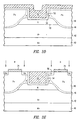
- Figure 2 shows in cross-section a transistor (DMOSFET) in accordance with the present invention. It is to be understood that this cross-section is drawn conventionally showing a portion of several cells of a typical transistor which may include thousands of such cells. However, a single cell transistor is also possible. Also while the present disclosure is directed to a transistor having a negatively (N) doped substrate, a positively (P) doped body region and an N doped source region, it is to be understood that complementary devices are also possible, wherein each dopant is reversed in terms of conductivity type.
- N negatively
- P positively
- the cross-sections shown here are not drawn to scale, but are intended to be illustrative. While the various transistor doped regions are shown here conventionally delineated by lines, this is illustrative rather than representative. In the figures, identical reference numbers used in various figures denote similar or identical structures. Also, the various parameters disclosed for junction depths, thicknesses, widths, doping concentrations, dosages and implantation energies are illustrative rather than limiting. Various materials may be used for the positive and negative type dopants. While the substances conventionally used for these doping types may be used, this is not limiting.
- Figure 2 therefore shows a cross-section of one cell, with small portions of adjoining cells, of the present transistor which includes a drain region 40 which is N+ doped so as to have a resistivity of 1 to 10 milliohm•cm and being of conventional thickness.
- a conventional metallized drain electrode (not shown) is formed on the bottom surface of drain region 40 as an electrical contact thereto.
- an N- doped epitaxial layer grown on the drain region 40 (substrate) is an N- doped epitaxial layer, the N-doped portions of which are designated 42. It is understood that region 42 may be formed other than by epitaxy.
- N- drift region 42 has a resistivity of 0.7 to 1.0 milliohm•cm.
- the epitaxial layer has a total thickness of 8 to 12 ⁇ m.
- a P doped tub 46 is formed in the upper portion of the semiconductor body.
- a typical doping level of P tub region is 1 X 10 16 to 1 X 10 17 /cm 3 . Thus, this is a relatively lightly doped region.
- a typical junction depth for the P tub 46 is 3 ⁇ m; a typical range is 2 to 4 ⁇ m.
- Formed inside the P doped tub 46 is the P+ doped body region 48.
- a typical doping level of the body region 48 is 1 X 10 18 /cm 3 to 5 X 10 18 g/cm 3 . Included as part of the P+ doped body region 48 is a lower P+ deep body portion at the lower portion of the body region.
- a typical junction depth of the P+ body region is 2.5 ⁇ m so as to be approximately 0.5 ⁇ m shallower than the surrounding P doped tub region 46.
- Penetrating downward from the principal surface of the semiconductor body is a set of trenches; one such trench 50 is illustrated.
- Trench 50 is lined, as are the others, by a gate oxide layer 54 which is typically 0.05 to 0.07 ⁇ m thick, and each trench is conventionally filled with a conductive doped polysilicon gate electrode gate 52.
- the P+ body region extends 0.5 ⁇ m below the bottom of the trench 50.
- N doped region 58 which underlies the trench 50 and also extends along the lower portion of the side walls of trench 50. Region 58 is called a JFET or pinch region.
- N doped region 58 advantageously further reduces the on-resistance of this transistor by creating a more heavily doped area at the lower side walls and bottom of the trench, compared to the underlying epitaxial drift region 42. Thus, this further reduces on-resistance by increasing the doping concentration in this region, which is typically where the parasitic JFET would form.
- a typical doping concentration of N doped region 58 is 1 X 10 15 /cm 3 . This doping concentration is optimized to maximize the trade-off between breakdown voltage and on-resistance.
- a typical thickness of N region 58 is about 0.5 ⁇ m. (This is the thickness between the floor of trench 50 and the uppermost portion of the underlying drift region 42.)
- N+ doped source regions 56 Formed in the upper portion of the transistor are N+ doped source regions 56 having a typical junction depth of 0.5 ⁇ m.
- a typical doping level of the N+ source regions 56 is about 6 X 10 19 /cm 3 at the principal surface.
- each conductive gate electrode 52 Insulating the upper portion of each conductive gate electrode 52 is a BPSG (boro-phosphosilicate glass) insulating layer 60 which is conventional and which is overlain by a body-source metallized layer 62.
- BPSG boro-phosphosilicate glass
- each transistor active part is surrounded by a termination at the principal surface of the semiconductor body, the termination typically including doped regions and sometimes a trench.
- Conventional terminations are suitable for use in accordance with the present invention, and hence the termination is not illustrated or further described herein.
- a typical width of each trench is 0.8 to 1.0 ⁇ m.
- a typical cell pitch is 10 ⁇ m but this is only illustrative.
- the cells may be of any one of various configurations.
- An N-doped epitaxial layer 42 is then grown thereon having a resistivity in the range of 0.7 to 1.0 milliohm•cm and a thickness of 6 to 11 ⁇ m.
- the upper portion of epitaxial layer 42 is then more heavily doped using an N type blanket implant to a final doping level of e.g. 1 X 10 15 /cm 3 .
- This implantation step is optimized to maximize the trade-off between breakdown voltage and on-resistance.
- a conventional masking layer is deposited and patterned to define the remaining portion 68.
- This mask layer 68 which is used to mask off subsequent the P type implant which forms the P tub regions 46.
- This P implant results in a final P doping concentration in the range of 10 16 to 10 17 /cm 3 , after a relatively long diffusion takes place at high temperature in order to drive in this P tub diffusion to a junction of 2 to 4 ⁇ m.
- This same step also drives in the previous N implant, which forms region 58 to a depth of 1 to 3 ⁇ m.
- a P+ implant forms the P+ regions 48.
- this may be a boron nitride or boron diffusion.
- This P+ implant results in a final doping concentration of 1 to 5 X 10 18 /cm 3 .
- the P tub region 46 surrounds (i.e. has a junction depth deeper than) the P+ region 48 after all drive in steps are completed.
- the principal surface of the semiconductor body has a conventional active mask layer formed thereon and patterned.
- This active mask may be oxide or other suitable material.
- This active mask defines the active portion of the transistor and hence masks off the transistor termination. It is to be understood that in the embodiments depicted herein only the active portion is shown, with the termination being outside the area of the drawing.
- a trench mask layer is then formed and patterned (not shown). Using the trench mask as a pattern, the trenches 50 are then etched anisotropically. The trenches are then subject to a sacrificial oxide step to smooth their sidewalls and bottoms. The gate oxide layer 54 is then grown conventionally to a thickness of 0.05 to 0.07 ⁇ m. A layer of polysilicon 52 is then formed on the principal surface of the semiconductive body and filling all the trenches. The polysilicon layer 52 is then doped to achieve maximum conductivity with an N type dopant (this step is not shown).
- a gate mask layer (polymask) is formed over the entire surface of the polysilicon, and patterned.
- the gate mask layer is then used to etch away the polysilicon except from the trenches while also leaving contact fingers on the principal surface connecting the gate electrodes in the various trenches (not shown).
- a source blocking mask 74 is formed on the principal surface of the substrate to define the regions where the source regions are to be formed.
- This masking layer 74 is conventionally patterned and then an N+ implant is carried out to define the N+ source regions 56.
- the N+ source mask layer 74 is then stripped.
- a layer of boro-phosphosilicate glass (BPSG) is conventionally deposited to a thickness of 1 to 1.5 ⁇ m and doped.
- a BPSG mask layer is then formed and patterned over the BPSG layer and then the BPSG mask layer is used to etch the BPSG, defining the BPSG regions 60 of Figure 2 insulating the top side of each conductive gate electrode 52.
- the BPSG mask layer is stripped, and a source-body metal layer is deposited and masked to define the source-body metallization contacts 62 of Figure 2.
- a passivation layer is formed and a pad mask is formed and patterned and use to define the pad contacts through the passivation layer (not shown). It is to be understood that the formation of the metal layer 62 has a corresponding step to form the contact to drain region 40 (not shown) on the back side of the substrate. This completes the transistor.
Claims (11)
- Structure de transistor, comprenant :un substrat semi-conducteur (40) d'un premier type de conductivité ;une zone de migration (42) recouvrant le substrat (40) et du premier type de conductivité, étant dopée à une concentration de dopage inférieure à celle du substrat (40) ;une zone en cuvette (46) d'un second type de conductivité, opposé au premier type de conductivité, et s'étendant depuis une surface supérieure de la structure de transistor en direction de la zone de migration (42) ;une zone de corps (48) du second type de conductivité dans la zone en cuvette (46), et étant dopée à une concentration supérieure à celle de la zone en cuvette (46), s'étendant depuis la surface supérieure en direction de la zone en cuvette (46) à une profondeur inférieure à celle de la zone en cuvette (46) ;une électrode de grille conductrice (52) s'étendant depuis la surface interne en direction de la zone de migration (42) à une profondeur moindre que celle de la zone en cuvette (46) ; etune zone source (56) du premier type de conductivité et s'étendant depuis la surface supérieure en direction de la zone en cuvette (46) et de la zone de corps (48) ;dans laquelle la zone en cuvette (46) entoure latéralement la zone de corps (48) ;
caractérisée en ce que
la zone de corps (48) s'étend plus profondément, depuis la surface supérieure, que ne le fait l'électrode de grille (52) ; et en ce que
la structure de transistor comprend en outre une zone de pincement (58) du premier type de conductivité, et de concentration de dopage supérieure à celle de la zone de migration (42), et située en position adjacente par rapport à une partie inférieure de l'électrode de grille (52), où la zone de pincement (58) s'étend de manière adjacente aux côtés et au fond de l'électrode de grille (52) et est éloignée du substrat (40) par une couche de zone de migration (42) s'intercalant, et une extension latérale et supérieure de la zone de pincement (58) est définie par la zone en cuvette (46) et la zone en cuvette (46) et la zone de corps (48) s'étendent en direction du substrat (40), depuis la surface supérieure, à une profondeur supérieure à celle de la zone de pincement (58). - Structure de transistor selon la revendication 1, dans laquelle la profondeur de jonction de la zone en cuvette (46) est d'environ 0,5 µm supérieure à la profondeur de la jonction de la zone de corps (48).
- Structure de transistor selon la revendication 1, dans laquelle une profondeur de la zone en cuvette (46) depuis la surface supérieure est d'au moins 2,5 µm.
- Structure de transistor selon la revendication 1, dans laquelle une concentration de dopage de la zone de corps (48) est d'au moins 10 fois celle de la zone en cuvette (46).
- Structure de transistor selon la revendication 1, dans laquelle une concentration de dopage de la zone en cuvette (46) est inférieure à 1 × 10¹⁷ /cm3.
- Procédé de formation de la structure de transistor selon l'une quelconque des revendications précédentes, comprenant les étapes suivantes à réaliser en série :(a) la fourniture d'un substrat de semi-conducteur (40) d'un premier type de conductivité ;(b) la formation d'une zone de migration (42) du premier type de conductivité et dopée à une concentration moindre que le substrat (40) et recouvrant le substrat (40) ;(c) la formation d'une zone de pincement (58) du premier type de conductivité en dopant une partie supérieure de la zone de migration (42) à une concentration supérieure à celle de la zone de migration (42) ;(d) la formation d'une couche de masquage (68) couvrant une partie de la zone de pincement (58) ;(e) la formation d'une zone en cuvette (46) d'un second type de conductivité, opposé au premier type de conductivité, et s'étendant depuis une surface supérieure de la zone de migration (42) en direction de la zone de migration (42) dans la partie de la zone de pincement (58) non couverte par la couche de masquage (68) ;(f) l'enfoncement simultané de la zone en cuvette (46) et de la zone de pincement (58) à leurs profondeurs de jonction désirée respectives ;(g) la formation d'une zone de corps (48) du second type de conductivité et de concentration de dopage supérieure à la zone en cuvette (46) et s'étendant depuis la surface supérieure en direction de la zone en cuvette (46) à une profondeur inférieure à celle de la zone en cuvette (46) et entourée latéralement par la zone en cuvette (46), en utilisant la couche de masquage (68), où une extension latérale et supérieure de la zone de pincement (58) est définie par la zone en cuvette (46), et la zone en cuvette (46) et la zone de corps (48) s'étendent en direction du substrat (40) depuis la surface supérieure à une profondeur supérieure à celle de la zone de pincement (58) ;(h) la formation d'une tranchée (50) s'étendant depuis la surface supérieure ;(i) la formation d'une électrode de grille conductrice (52) dans la tranchée (50) de manière à ce que la zone de pincement (58) s'étende en position adjacente par rapport aux côtés et au fond de l'électrode de grille (52) et la zone de corps (48) et la zone en cuvette (46) s'étendent chacune plus profondément depuis la surface supérieure, que ne le fait l'électrode de grille (52) ; et(j) la formation d'une zone source (56) du premier type de conductivité s'étendant depuis la surface supérieure dans la direction de la zone du corps (48).
- Procédé selon la revendication 6, dans lequel l'étape de formation de la zone en cuvette (46) comprend :l'implantation d'ions du second type de conductivité ; etla diffusion des ions implantés à une profondeur d'au moins 2 µm par rapport à la surface supérieure.
- Procédé selon la revendication 6, dans lequel la profondeur de jonction de la zone en cuvette (46) est d'environ 0,5 µm supérieure à celle de la profondeur de jonction de la zone de corps (48).
- Procédé selon la revendication 6, dans lequel la profondeur de jonction de la zone en cuvette (46) est d'au moins 2,5 µm.
- Procédé selon la revendication 6, dans lequel une concentration de dopage dans la zone de corps (48) est d'au moins 10 fois celle de la zone en cuvette (46).
- Procédé selon la revendication 6, dans lequel une concentration de dopage de la zone en cuvette (46) est inférieure à 1 × 10¹⁷ /cm3.
Applications Claiming Priority (3)
| Application Number | Priority Date | Filing Date | Title |
|---|---|---|---|
| US610563 | 1996-03-06 | ||
| US08/610,563 US5821583A (en) | 1996-03-06 | 1996-03-06 | Trenched DMOS transistor with lightly doped tub |
| PCT/US1997/002974 WO1997033320A1 (fr) | 1996-03-06 | 1997-03-05 | Transistors dmos a tranchee avec une cuvette legerement dopee |
Publications (3)
| Publication Number | Publication Date |
|---|---|
| EP0885460A1 EP0885460A1 (fr) | 1998-12-23 |
| EP0885460A4 EP0885460A4 (fr) | 1999-05-12 |
| EP0885460B1 true EP0885460B1 (fr) | 2006-03-01 |
Family
ID=24445538
Family Applications (1)
| Application Number | Title | Priority Date | Filing Date |
|---|---|---|---|
| EP97908734A Expired - Lifetime EP0885460B1 (fr) | 1996-03-06 | 1997-03-05 | Transistor dmos a tranchee ayant une cuvette faiblement dopee |
Country Status (5)
| Country | Link |
|---|---|
| US (1) | US5821583A (fr) |
| EP (1) | EP0885460B1 (fr) |
| AU (1) | AU2057097A (fr) |
| DE (1) | DE69735349T2 (fr) |
| WO (1) | WO1997033320A1 (fr) |
Families Citing this family (35)
| Publication number | Priority date | Publication date | Assignee | Title |
|---|---|---|---|---|
| AU3724197A (en) * | 1996-07-19 | 1998-02-10 | Siliconix Incorporated | High density trench dmos transistor with trench bottom implant |
| KR100218260B1 (ko) * | 1997-01-14 | 1999-09-01 | 김덕중 | 트랜치 게이트형 모스트랜지스터의 제조방법 |
| US6163052A (en) * | 1997-04-04 | 2000-12-19 | Advanced Micro Devices, Inc. | Trench-gated vertical combination JFET and MOSFET devices |
| JP3219045B2 (ja) * | 1998-02-20 | 2001-10-15 | 日本電気株式会社 | 縦型misfetの製造方法 |
| US6084264A (en) * | 1998-11-25 | 2000-07-04 | Siliconix Incorporated | Trench MOSFET having improved breakdown and on-resistance characteristics |
| JP4017826B2 (ja) | 1998-12-18 | 2007-12-05 | インフィネオン テクノロジース アクチエンゲゼルシャフト | 溝形のゲート電極を有する電界効果型トランジスタセルデバイス |
| DE19908809B4 (de) | 1999-03-01 | 2007-02-01 | Infineon Technologies Ag | Verfahren zur Herstellung einer MOS-Transistorstruktur mit einstellbarer Schwellspannung |
| US6472678B1 (en) * | 2000-06-16 | 2002-10-29 | General Semiconductor, Inc. | Trench MOSFET with double-diffused body profile |
| US7291884B2 (en) * | 2001-07-03 | 2007-11-06 | Siliconix Incorporated | Trench MIS device having implanted drain-drift region and thick bottom oxide |
| US7009247B2 (en) * | 2001-07-03 | 2006-03-07 | Siliconix Incorporated | Trench MIS device with thick oxide layer in bottom of gate contact trench |
| US7033876B2 (en) * | 2001-07-03 | 2006-04-25 | Siliconix Incorporated | Trench MIS device having implanted drain-drift region and thick bottom oxide and process for manufacturing the same |
| US20060038223A1 (en) * | 2001-07-03 | 2006-02-23 | Siliconix Incorporated | Trench MOSFET having drain-drift region comprising stack of implanted regions |
| US20030151092A1 (en) * | 2002-02-11 | 2003-08-14 | Feng-Tso Chien | Power mosfet device with reduced snap-back and being capable of increasing avalanche-breakdown current endurance, and method of manafacturing the same |
| US7576388B1 (en) | 2002-10-03 | 2009-08-18 | Fairchild Semiconductor Corporation | Trench-gate LDMOS structures |
| US7638841B2 (en) | 2003-05-20 | 2009-12-29 | Fairchild Semiconductor Corporation | Power semiconductor devices and methods of manufacture |
| JP3954541B2 (ja) * | 2003-08-05 | 2007-08-08 | 株式会社東芝 | 半導体装置及びその製造方法 |
| US7368777B2 (en) | 2003-12-30 | 2008-05-06 | Fairchild Semiconductor Corporation | Accumulation device with charge balance structure and method of forming the same |
| US7352036B2 (en) | 2004-08-03 | 2008-04-01 | Fairchild Semiconductor Corporation | Semiconductor power device having a top-side drain using a sinker trench |
| KR100624053B1 (ko) * | 2004-09-09 | 2006-09-15 | 라이톤 세미컨덕터 코퍼레이션 | 펀치스루를 방지하기 위한 전력용 반도체 소자 및 그 제조방법 |
| CN101882583A (zh) | 2005-04-06 | 2010-11-10 | 飞兆半导体公司 | 沟栅场效应晶体管及其形成方法 |
| CN101542731B (zh) * | 2005-05-26 | 2012-07-11 | 飞兆半导体公司 | 沟槽栅场效应晶体管及其制造方法 |
| US7446374B2 (en) | 2006-03-24 | 2008-11-04 | Fairchild Semiconductor Corporation | High density trench FET with integrated Schottky diode and method of manufacture |
| US7319256B1 (en) | 2006-06-19 | 2008-01-15 | Fairchild Semiconductor Corporation | Shielded gate trench FET with the shield and gate electrodes being connected together |
| US7772668B2 (en) | 2007-12-26 | 2010-08-10 | Fairchild Semiconductor Corporation | Shielded gate trench FET with multiple channels |
| WO2009102684A2 (fr) | 2008-02-14 | 2009-08-20 | Maxpower Semiconductor Inc. | Structures de dispositifs à semi-conducteurs et procédés s'y rapportant |
| US8704295B1 (en) | 2008-02-14 | 2014-04-22 | Maxpower Semiconductor, Inc. | Schottky and MOSFET+Schottky structures, devices, and methods |
| US8174067B2 (en) | 2008-12-08 | 2012-05-08 | Fairchild Semiconductor Corporation | Trench-based power semiconductor devices with increased breakdown voltage characteristics |
| US8432000B2 (en) | 2010-06-18 | 2013-04-30 | Fairchild Semiconductor Corporation | Trench MOS barrier schottky rectifier with a planar surface using CMP techniques |
| US9685523B2 (en) * | 2014-12-17 | 2017-06-20 | Alpha And Omega Semiconductor Incorporated | Diode structures with controlled injection efficiency for fast switching |
| JP5498431B2 (ja) * | 2011-02-02 | 2014-05-21 | ローム株式会社 | 半導体装置およびその製造方法 |
| EP3024018B1 (fr) * | 2013-07-19 | 2018-08-08 | Nissan Motor Co., Ltd | Dispositif à semi-conducteurs |
| US20150118810A1 (en) * | 2013-10-24 | 2015-04-30 | Madhur Bobde | Buried field ring field effect transistor (buf-fet) integrated with cells implanted with hole supply path |
| JP6584857B2 (ja) * | 2015-08-11 | 2019-10-02 | 株式会社東芝 | 半導体装置 |
| JP7458217B2 (ja) | 2020-03-19 | 2024-03-29 | 株式会社東芝 | 半導体装置、半導体装置の製造方法、インバータ回路、駆動装置、車両、及び、昇降機 |
| CN116646391A (zh) * | 2023-07-26 | 2023-08-25 | 深圳市锐骏半导体股份有限公司 | 一种沟槽功率器件及其制造方法 |
Family Cites Families (22)
| Publication number | Priority date | Publication date | Assignee | Title |
|---|---|---|---|---|
| JPS5658267A (en) * | 1979-10-17 | 1981-05-21 | Nippon Telegr & Teleph Corp <Ntt> | Insulated gate type field-effect transistor |
| IT1154298B (it) * | 1981-02-23 | 1987-01-21 | Motorola Inc | Perfezionemento nei transistori di potenza mos |
| US4893160A (en) * | 1987-11-13 | 1990-01-09 | Siliconix Incorporated | Method for increasing the performance of trenched devices and the resulting structure |
| US5072266A (en) * | 1988-12-27 | 1991-12-10 | Siliconix Incorporated | Trench DMOS power transistor with field-shaping body profile and three-dimensional geometry |
| US4931408A (en) * | 1989-10-13 | 1990-06-05 | Siliconix Incorporated | Method of fabricating a short-channel low voltage DMOS transistor |
| JP2504862B2 (ja) * | 1990-10-08 | 1996-06-05 | 三菱電機株式会社 | 半導体装置及びその製造方法 |
| US5304831A (en) * | 1990-12-21 | 1994-04-19 | Siliconix Incorporated | Low on-resistance power MOS technology |
| US5404040A (en) * | 1990-12-21 | 1995-04-04 | Siliconix Incorporated | Structure and fabrication of power MOSFETs, including termination structures |
| US5168331A (en) * | 1991-01-31 | 1992-12-01 | Siliconix Incorporated | Power metal-oxide-semiconductor field effect transistor |
| US5248627A (en) * | 1992-03-20 | 1993-09-28 | Siliconix Incorporated | Threshold adjustment in fabricating vertical dmos devices |
| US5910669A (en) * | 1992-07-24 | 1999-06-08 | Siliconix Incorporated | Field effect Trench transistor having lightly doped epitaxial region on the surface portion thereof |
| US5558313A (en) * | 1992-07-24 | 1996-09-24 | Siliconix Inorporated | Trench field effect transistor with reduced punch-through susceptibility and low RDSon |
| JPH06104445A (ja) * | 1992-08-04 | 1994-04-15 | Siliconix Inc | 電力用mosトランジスタ及びその製造方法 |
| US5316959A (en) * | 1992-08-12 | 1994-05-31 | Siliconix, Incorporated | Trenched DMOS transistor fabrication using six masks |
| US5341011A (en) * | 1993-03-15 | 1994-08-23 | Siliconix Incorporated | Short channel trenched DMOS transistor |
| US5410170A (en) * | 1993-04-14 | 1995-04-25 | Siliconix Incorporated | DMOS power transistors with reduced number of contacts using integrated body-source connections |
| US5468982A (en) * | 1994-06-03 | 1995-11-21 | Siliconix Incorporated | Trenched DMOS transistor with channel block at cell trench corners |
| US5486772A (en) * | 1994-06-30 | 1996-01-23 | Siliconix Incorporation | Reliability test method for semiconductor trench devices |
| US5688725A (en) * | 1994-12-30 | 1997-11-18 | Siliconix Incorporated | Method of making a trench mosfet with heavily doped delta layer to provide low on-resistance |
| JPH08306914A (ja) * | 1995-04-27 | 1996-11-22 | Nippondenso Co Ltd | 半導体装置およびその製造方法 |
| US5567634A (en) * | 1995-05-01 | 1996-10-22 | National Semiconductor Corporation | Method of fabricating self-aligned contact trench DMOS transistors |
| US5689128A (en) * | 1995-08-21 | 1997-11-18 | Siliconix Incorporated | High density trenched DMOS transistor |
-
1996
- 1996-03-06 US US08/610,563 patent/US5821583A/en not_active Expired - Lifetime
-
1997
- 1997-03-05 WO PCT/US1997/002974 patent/WO1997033320A1/fr active IP Right Grant
- 1997-03-05 DE DE69735349T patent/DE69735349T2/de not_active Expired - Lifetime
- 1997-03-05 EP EP97908734A patent/EP0885460B1/fr not_active Expired - Lifetime
- 1997-03-05 AU AU20570/97A patent/AU2057097A/en not_active Abandoned
Also Published As
| Publication number | Publication date |
|---|---|
| AU2057097A (en) | 1997-09-22 |
| US5821583A (en) | 1998-10-13 |
| EP0885460A1 (fr) | 1998-12-23 |
| DE69735349D1 (de) | 2006-04-27 |
| WO1997033320A1 (fr) | 1997-09-12 |
| EP0885460A4 (fr) | 1999-05-12 |
| DE69735349T2 (de) | 2006-11-30 |
Similar Documents
| Publication | Publication Date | Title |
|---|---|---|
| EP0885460B1 (fr) | Transistor dmos a tranchee ayant une cuvette faiblement dopee | |
| EP2043158B1 (fr) | Transistor dmos à tranchée ayant une implantation de fond de tranchée | |
| US6566201B1 (en) | Method for fabricating a high voltage power MOSFET having a voltage sustaining region that includes doped columns formed by rapid diffusion | |
| US7084455B2 (en) | Power semiconductor device having a voltage sustaining region that includes terraced trench with continuous doped columns formed in an epitaxial layer | |
| EP1292990B1 (fr) | Transistor mos a tranchees avec profil de corps a double diffusion | |
| US6992350B2 (en) | High voltage power MOSFET having low on-resistance | |
| US7091552B2 (en) | High voltage power MOSFET having a voltage sustaining region that includes doped columns formed by trench etching and ion implantation | |
| US7019360B2 (en) | High voltage power mosfet having a voltage sustaining region that includes doped columns formed by trench etching using an etchant gas that is also a doping source | |
| EP2178125A2 (fr) | Transistor à effet de champ avec tranchée et sa méthode de fabrication | |
| EP0958611A1 (fr) | Transistor dmos haute densite |
Legal Events
| Date | Code | Title | Description |
|---|---|---|---|
| PUAI | Public reference made under article 153(3) epc to a published international application that has entered the european phase |
Free format text: ORIGINAL CODE: 0009012 |
|
| 17P | Request for examination filed |
Effective date: 19980819 |
|
| AK | Designated contracting states |
Kind code of ref document: A1 Designated state(s): DE FR IT NL |
|
| A4 | Supplementary search report drawn up and despatched |
Effective date: 19990326 |
|
| AK | Designated contracting states |
Kind code of ref document: A4 Designated state(s): DE FR IT NL |
|
| RHK1 | Main classification (correction) |
Ipc: H01L 29/78 |
|
| 17Q | First examination report despatched |
Effective date: 20000214 |
|
| GRAP | Despatch of communication of intention to grant a patent |
Free format text: ORIGINAL CODE: EPIDOSNIGR1 |
|
| GRAS | Grant fee paid |
Free format text: ORIGINAL CODE: EPIDOSNIGR3 |
|
| GRAA | (expected) grant |
Free format text: ORIGINAL CODE: 0009210 |
|
| AK | Designated contracting states |
Kind code of ref document: B1 Designated state(s): DE FR IT NL |
|
| PG25 | Lapsed in a contracting state [announced via postgrant information from national office to epo] |
Ref country code: NL Free format text: LAPSE BECAUSE OF FAILURE TO SUBMIT A TRANSLATION OF THE DESCRIPTION OR TO PAY THE FEE WITHIN THE PRESCRIBED TIME-LIMIT Effective date: 20060301 Ref country code: IT Free format text: LAPSE BECAUSE OF FAILURE TO SUBMIT A TRANSLATION OF THE DESCRIPTION OR TO PAY THE FEE WITHIN THE PRESCRIBED TIME-LIMIT;WARNING: LAPSES OF ITALIAN PATENTS WITH EFFECTIVE DATE BEFORE 2007 MAY HAVE OCCURRED AT ANY TIME BEFORE 2007. THE CORRECT EFFECTIVE DATE MAY BE DIFFERENT FROM THE ONE RECORDED. Effective date: 20060301 |
|
| REF | Corresponds to: |
Ref document number: 69735349 Country of ref document: DE Date of ref document: 20060427 Kind code of ref document: P |
|
| NLV1 | Nl: lapsed or annulled due to failure to fulfill the requirements of art. 29p and 29m of the patents act | ||
| PLBE | No opposition filed within time limit |
Free format text: ORIGINAL CODE: 0009261 |
|
| STAA | Information on the status of an ep patent application or granted ep patent |
Free format text: STATUS: NO OPPOSITION FILED WITHIN TIME LIMIT |
|
| 26N | No opposition filed |
Effective date: 20061204 |
|
| EN | Fr: translation not filed | ||
| PGFP | Annual fee paid to national office [announced via postgrant information from national office to epo] |
Ref country code: FR Payment date: 20070319 Year of fee payment: 11 |
|
| PG25 | Lapsed in a contracting state [announced via postgrant information from national office to epo] |
Ref country code: FR Free format text: LAPSE BECAUSE OF NON-PAYMENT OF DUE FEES Effective date: 20080330 |
|
| PGFP | Annual fee paid to national office [announced via postgrant information from national office to epo] |
Ref country code: DE Payment date: 20150327 Year of fee payment: 19 |
|
| REG | Reference to a national code |
Ref country code: DE Ref legal event code: R119 Ref document number: 69735349 Country of ref document: DE |
|
| PG25 | Lapsed in a contracting state [announced via postgrant information from national office to epo] |
Ref country code: DE Free format text: LAPSE BECAUSE OF NON-PAYMENT OF DUE FEES Effective date: 20161001 |