EP0715355A2 - Kappe zum Verschliessen von Vialöchern in LPL - Google Patents
Kappe zum Verschliessen von Vialöchern in LPL Download PDFInfo
- Publication number
- EP0715355A2 EP0715355A2 EP95117631A EP95117631A EP0715355A2 EP 0715355 A2 EP0715355 A2 EP 0715355A2 EP 95117631 A EP95117631 A EP 95117631A EP 95117631 A EP95117631 A EP 95117631A EP 0715355 A2 EP0715355 A2 EP 0715355A2
- Authority
- EP
- European Patent Office
- Prior art keywords
- electrically conducting
- plane
- photosensitive material
- layer
- plated
- Prior art date
- Legal status (The legal status is an assumption and is not a legal conclusion. Google has not performed a legal analysis and makes no representation as to the accuracy of the status listed.)
- Withdrawn
Links
- 150000003071 polychlorinated biphenyls Chemical class 0.000 title 1
- 239000004020 conductor Substances 0.000 claims abstract description 70
- 238000000034 method Methods 0.000 claims abstract description 44
- 239000002131 composite material Substances 0.000 claims abstract description 42
- 229910000679 solder Inorganic materials 0.000 claims abstract description 37
- 239000012777 electrically insulating material Substances 0.000 claims abstract description 12
- 239000000463 material Substances 0.000 claims description 64
- 230000005855 radiation Effects 0.000 claims description 17
- 238000000151 deposition Methods 0.000 claims description 10
- 238000006552 photochemical reaction Methods 0.000 claims description 6
- 238000007789 sealing Methods 0.000 claims description 6
- 238000005530 etching Methods 0.000 claims description 4
- 238000010030 laminating Methods 0.000 claims description 3
- 238000004140 cleaning Methods 0.000 claims 2
- RYGMFSIKBFXOCR-UHFFFAOYSA-N Copper Chemical compound [Cu] RYGMFSIKBFXOCR-UHFFFAOYSA-N 0.000 description 10
- 229910052802 copper Inorganic materials 0.000 description 9
- 239000010949 copper Substances 0.000 description 9
- 238000007747 plating Methods 0.000 description 6
- 239000004065 semiconductor Substances 0.000 description 5
- PCHJSUWPFVWCPO-UHFFFAOYSA-N gold Chemical compound [Au] PCHJSUWPFVWCPO-UHFFFAOYSA-N 0.000 description 4
- 229910052737 gold Inorganic materials 0.000 description 4
- 239000010931 gold Substances 0.000 description 4
- 239000002184 metal Substances 0.000 description 3
- 229910052751 metal Inorganic materials 0.000 description 3
- NLXLAEXVIDQMFP-UHFFFAOYSA-N Ammonia chloride Chemical compound [NH4+].[Cl-] NLXLAEXVIDQMFP-UHFFFAOYSA-N 0.000 description 2
- 229910001374 Invar Inorganic materials 0.000 description 2
- ORTQZVOHEJQUHG-UHFFFAOYSA-L copper(II) chloride Chemical compound Cl[Cu]Cl ORTQZVOHEJQUHG-UHFFFAOYSA-L 0.000 description 2
- 230000003247 decreasing effect Effects 0.000 description 2
- 239000003989 dielectric material Substances 0.000 description 2
- 239000011888 foil Substances 0.000 description 2
- 238000004544 sputter deposition Methods 0.000 description 2
- ATJFFYVFTNAWJD-UHFFFAOYSA-N Tin Chemical compound [Sn] ATJFFYVFTNAWJD-UHFFFAOYSA-N 0.000 description 1
- 239000000654 additive Substances 0.000 description 1
- 235000019270 ammonium chloride Nutrition 0.000 description 1
- 239000000969 carrier Substances 0.000 description 1
- 239000011889 copper foil Substances 0.000 description 1
- 229960003280 cupric chloride Drugs 0.000 description 1
- 238000005553 drilling Methods 0.000 description 1
- 238000009713 electroplating Methods 0.000 description 1
- 238000005516 engineering process Methods 0.000 description 1
- 238000003475 lamination Methods 0.000 description 1
- 150000002739 metals Chemical class 0.000 description 1
- 238000012986 modification Methods 0.000 description 1
- 230000004048 modification Effects 0.000 description 1
- 238000010943 off-gassing Methods 0.000 description 1
- 239000000126 substance Substances 0.000 description 1
Images
Classifications
-
- H—ELECTRICITY
- H01—ELECTRIC ELEMENTS
- H01L—SEMICONDUCTOR DEVICES NOT COVERED BY CLASS H10
- H01L23/00—Details of semiconductor or other solid state devices
- H01L23/48—Arrangements for conducting electric current to or from the solid state body in operation, e.g. leads, terminal arrangements ; Selection of materials therefor
- H01L23/488—Arrangements for conducting electric current to or from the solid state body in operation, e.g. leads, terminal arrangements ; Selection of materials therefor consisting of soldered or bonded constructions
- H01L23/498—Leads, i.e. metallisations or lead-frames on insulating substrates, e.g. chip carriers
- H01L23/49827—Via connections through the substrates, e.g. pins going through the substrate, coaxial cables
-
- H—ELECTRICITY
- H01—ELECTRIC ELEMENTS
- H01L—SEMICONDUCTOR DEVICES NOT COVERED BY CLASS H10
- H01L21/00—Processes or apparatus adapted for the manufacture or treatment of semiconductor or solid state devices or of parts thereof
- H01L21/02—Manufacture or treatment of semiconductor devices or of parts thereof
- H01L21/04—Manufacture or treatment of semiconductor devices or of parts thereof the devices having potential barriers, e.g. a PN junction, depletion layer or carrier concentration layer
- H01L21/48—Manufacture or treatment of parts, e.g. containers, prior to assembly of the devices, using processes not provided for in a single one of the groups H01L21/18 - H01L21/326 or H10D48/04 - H10D48/07
- H01L21/4814—Conductive parts
- H01L21/4846—Leads on or in insulating or insulated substrates, e.g. metallisation
- H01L21/486—Via connections through the substrate with or without pins
-
- H—ELECTRICITY
- H01—ELECTRIC ELEMENTS
- H01L—SEMICONDUCTOR DEVICES NOT COVERED BY CLASS H10
- H01L23/00—Details of semiconductor or other solid state devices
- H01L23/48—Arrangements for conducting electric current to or from the solid state body in operation, e.g. leads, terminal arrangements ; Selection of materials therefor
- H01L23/488—Arrangements for conducting electric current to or from the solid state body in operation, e.g. leads, terminal arrangements ; Selection of materials therefor consisting of soldered or bonded constructions
- H01L23/498—Leads, i.e. metallisations or lead-frames on insulating substrates, e.g. chip carriers
- H01L23/49833—Leads, i.e. metallisations or lead-frames on insulating substrates, e.g. chip carriers the chip support structure consisting of a plurality of insulating substrates
-
- H—ELECTRICITY
- H01—ELECTRIC ELEMENTS
- H01L—SEMICONDUCTOR DEVICES NOT COVERED BY CLASS H10
- H01L23/00—Details of semiconductor or other solid state devices
- H01L23/52—Arrangements for conducting electric current within the device in operation from one component to another, i.e. interconnections, e.g. wires, lead frames
- H01L23/538—Arrangements for conducting electric current within the device in operation from one component to another, i.e. interconnections, e.g. wires, lead frames the interconnection structure between a plurality of semiconductor chips being formed on, or in, insulating substrates
- H01L23/5384—Conductive vias through the substrate with or without pins, e.g. buried coaxial conductors
-
- H—ELECTRICITY
- H01—ELECTRIC ELEMENTS
- H01L—SEMICONDUCTOR DEVICES NOT COVERED BY CLASS H10
- H01L23/00—Details of semiconductor or other solid state devices
- H01L23/52—Arrangements for conducting electric current within the device in operation from one component to another, i.e. interconnections, e.g. wires, lead frames
- H01L23/538—Arrangements for conducting electric current within the device in operation from one component to another, i.e. interconnections, e.g. wires, lead frames the interconnection structure between a plurality of semiconductor chips being formed on, or in, insulating substrates
- H01L23/5385—Assembly of a plurality of insulating substrates
-
- H—ELECTRICITY
- H05—ELECTRIC TECHNIQUES NOT OTHERWISE PROVIDED FOR
- H05K—PRINTED CIRCUITS; CASINGS OR CONSTRUCTIONAL DETAILS OF ELECTRIC APPARATUS; MANUFACTURE OF ASSEMBLAGES OF ELECTRICAL COMPONENTS
- H05K1/00—Printed circuits
- H05K1/02—Details
- H05K1/11—Printed elements for providing electric connections to or between printed circuits
- H05K1/111—Pads for surface mounting, e.g. lay-out
- H05K1/112—Pads for surface mounting, e.g. lay-out directly combined with via connections
- H05K1/113—Via provided in pad; Pad over filled via
-
- H—ELECTRICITY
- H05—ELECTRIC TECHNIQUES NOT OTHERWISE PROVIDED FOR
- H05K—PRINTED CIRCUITS; CASINGS OR CONSTRUCTIONAL DETAILS OF ELECTRIC APPARATUS; MANUFACTURE OF ASSEMBLAGES OF ELECTRICAL COMPONENTS
- H05K3/00—Apparatus or processes for manufacturing printed circuits
- H05K3/0094—Filling or covering plated through-holes or blind plated vias, e.g. for masking or for mechanical reinforcement
-
- H—ELECTRICITY
- H05—ELECTRIC TECHNIQUES NOT OTHERWISE PROVIDED FOR
- H05K—PRINTED CIRCUITS; CASINGS OR CONSTRUCTIONAL DETAILS OF ELECTRIC APPARATUS; MANUFACTURE OF ASSEMBLAGES OF ELECTRICAL COMPONENTS
- H05K3/00—Apparatus or processes for manufacturing printed circuits
- H05K3/40—Forming printed elements for providing electric connections to or between printed circuits
- H05K3/4007—Surface contacts, e.g. bumps
- H05K3/4015—Surface contacts, e.g. bumps using auxiliary conductive elements, e.g. pieces of metal foil, metallic spheres
-
- H—ELECTRICITY
- H01—ELECTRIC ELEMENTS
- H01L—SEMICONDUCTOR DEVICES NOT COVERED BY CLASS H10
- H01L2224/00—Indexing scheme for arrangements for connecting or disconnecting semiconductor or solid-state bodies and methods related thereto as covered by H01L24/00
- H01L2224/01—Means for bonding being attached to, or being formed on, the surface to be connected, e.g. chip-to-package, die-attach, "first-level" interconnects; Manufacturing methods related thereto
- H01L2224/10—Bump connectors; Manufacturing methods related thereto
- H01L2224/15—Structure, shape, material or disposition of the bump connectors after the connecting process
- H01L2224/16—Structure, shape, material or disposition of the bump connectors after the connecting process of an individual bump connector
- H01L2224/161—Disposition
- H01L2224/16151—Disposition the bump connector connecting between a semiconductor or solid-state body and an item not being a semiconductor or solid-state body, e.g. chip-to-substrate, chip-to-passive
- H01L2224/16221—Disposition the bump connector connecting between a semiconductor or solid-state body and an item not being a semiconductor or solid-state body, e.g. chip-to-substrate, chip-to-passive the body and the item being stacked
- H01L2224/16225—Disposition the bump connector connecting between a semiconductor or solid-state body and an item not being a semiconductor or solid-state body, e.g. chip-to-substrate, chip-to-passive the body and the item being stacked the item being non-metallic, e.g. insulating substrate with or without metallisation
-
- H—ELECTRICITY
- H01—ELECTRIC ELEMENTS
- H01L—SEMICONDUCTOR DEVICES NOT COVERED BY CLASS H10
- H01L2924/00—Indexing scheme for arrangements or methods for connecting or disconnecting semiconductor or solid-state bodies as covered by H01L24/00
- H01L2924/01—Chemical elements
- H01L2924/01019—Potassium [K]
-
- H—ELECTRICITY
- H01—ELECTRIC ELEMENTS
- H01L—SEMICONDUCTOR DEVICES NOT COVERED BY CLASS H10
- H01L2924/00—Indexing scheme for arrangements or methods for connecting or disconnecting semiconductor or solid-state bodies as covered by H01L24/00
- H01L2924/01—Chemical elements
- H01L2924/01078—Platinum [Pt]
-
- H—ELECTRICITY
- H01—ELECTRIC ELEMENTS
- H01L—SEMICONDUCTOR DEVICES NOT COVERED BY CLASS H10
- H01L2924/00—Indexing scheme for arrangements or methods for connecting or disconnecting semiconductor or solid-state bodies as covered by H01L24/00
- H01L2924/01—Chemical elements
- H01L2924/01079—Gold [Au]
-
- H—ELECTRICITY
- H01—ELECTRIC ELEMENTS
- H01L—SEMICONDUCTOR DEVICES NOT COVERED BY CLASS H10
- H01L2924/00—Indexing scheme for arrangements or methods for connecting or disconnecting semiconductor or solid-state bodies as covered by H01L24/00
- H01L2924/15—Details of package parts other than the semiconductor or other solid state devices to be connected
- H01L2924/151—Die mounting substrate
- H01L2924/153—Connection portion
- H01L2924/1531—Connection portion the connection portion being formed only on the surface of the substrate opposite to the die mounting surface
- H01L2924/15313—Connection portion the connection portion being formed only on the surface of the substrate opposite to the die mounting surface being a land array, e.g. LGA
-
- H—ELECTRICITY
- H05—ELECTRIC TECHNIQUES NOT OTHERWISE PROVIDED FOR
- H05K—PRINTED CIRCUITS; CASINGS OR CONSTRUCTIONAL DETAILS OF ELECTRIC APPARATUS; MANUFACTURE OF ASSEMBLAGES OF ELECTRICAL COMPONENTS
- H05K2201/00—Indexing scheme relating to printed circuits covered by H05K1/00
- H05K2201/09—Shape and layout
- H05K2201/09209—Shape and layout details of conductors
- H05K2201/095—Conductive through-holes or vias
- H05K2201/096—Vertically aligned vias, holes or stacked vias
-
- H—ELECTRICITY
- H05—ELECTRIC TECHNIQUES NOT OTHERWISE PROVIDED FOR
- H05K—PRINTED CIRCUITS; CASINGS OR CONSTRUCTIONAL DETAILS OF ELECTRIC APPARATUS; MANUFACTURE OF ASSEMBLAGES OF ELECTRICAL COMPONENTS
- H05K2201/00—Indexing scheme relating to printed circuits covered by H05K1/00
- H05K2201/10—Details of components or other objects attached to or integrated in a printed circuit board
- H05K2201/10613—Details of electrical connections of non-printed components, e.g. special leads
- H05K2201/10621—Components characterised by their electrical contacts
- H05K2201/10734—Ball grid array [BGA]; Bump grid array
-
- H—ELECTRICITY
- H05—ELECTRIC TECHNIQUES NOT OTHERWISE PROVIDED FOR
- H05K—PRINTED CIRCUITS; CASINGS OR CONSTRUCTIONAL DETAILS OF ELECTRIC APPARATUS; MANUFACTURE OF ASSEMBLAGES OF ELECTRICAL COMPONENTS
- H05K2203/00—Indexing scheme relating to apparatus or processes for manufacturing printed circuits covered by H05K3/00
- H05K2203/13—Moulding and encapsulation; Deposition techniques; Protective layers
- H05K2203/1377—Protective layers
- H05K2203/1394—Covering open PTHs, e.g. by dry film resist or by metal disc
-
- H—ELECTRICITY
- H05—ELECTRIC TECHNIQUES NOT OTHERWISE PROVIDED FOR
- H05K—PRINTED CIRCUITS; CASINGS OR CONSTRUCTIONAL DETAILS OF ELECTRIC APPARATUS; MANUFACTURE OF ASSEMBLAGES OF ELECTRICAL COMPONENTS
- H05K3/00—Apparatus or processes for manufacturing printed circuits
- H05K3/02—Apparatus or processes for manufacturing printed circuits in which the conductive material is applied to the surface of the insulating support and is thereafter removed from such areas of the surface which are not intended for current conducting or shielding
- H05K3/06—Apparatus or processes for manufacturing printed circuits in which the conductive material is applied to the surface of the insulating support and is thereafter removed from such areas of the surface which are not intended for current conducting or shielding the conductive material being removed chemically or electrolytically, e.g. by photo-etch process
- H05K3/061—Etching masks
- H05K3/062—Etching masks consisting of metals or alloys or metallic inorganic compounds
-
- H—ELECTRICITY
- H05—ELECTRIC TECHNIQUES NOT OTHERWISE PROVIDED FOR
- H05K—PRINTED CIRCUITS; CASINGS OR CONSTRUCTIONAL DETAILS OF ELECTRIC APPARATUS; MANUFACTURE OF ASSEMBLAGES OF ELECTRICAL COMPONENTS
- H05K3/00—Apparatus or processes for manufacturing printed circuits
- H05K3/02—Apparatus or processes for manufacturing printed circuits in which the conductive material is applied to the surface of the insulating support and is thereafter removed from such areas of the surface which are not intended for current conducting or shielding
- H05K3/06—Apparatus or processes for manufacturing printed circuits in which the conductive material is applied to the surface of the insulating support and is thereafter removed from such areas of the surface which are not intended for current conducting or shielding the conductive material being removed chemically or electrolytically, e.g. by photo-etch process
- H05K3/061—Etching masks
- H05K3/064—Photoresists
-
- H—ELECTRICITY
- H05—ELECTRIC TECHNIQUES NOT OTHERWISE PROVIDED FOR
- H05K—PRINTED CIRCUITS; CASINGS OR CONSTRUCTIONAL DETAILS OF ELECTRIC APPARATUS; MANUFACTURE OF ASSEMBLAGES OF ELECTRICAL COMPONENTS
- H05K3/00—Apparatus or processes for manufacturing printed circuits
- H05K3/10—Apparatus or processes for manufacturing printed circuits in which conductive material is applied to the insulating support in such a manner as to form the desired conductive pattern
- H05K3/20—Apparatus or processes for manufacturing printed circuits in which conductive material is applied to the insulating support in such a manner as to form the desired conductive pattern by affixing prefabricated conductor pattern
- H05K3/205—Apparatus or processes for manufacturing printed circuits in which conductive material is applied to the insulating support in such a manner as to form the desired conductive pattern by affixing prefabricated conductor pattern using a pattern electroplated or electroformed on a metallic carrier
-
- H—ELECTRICITY
- H05—ELECTRIC TECHNIQUES NOT OTHERWISE PROVIDED FOR
- H05K—PRINTED CIRCUITS; CASINGS OR CONSTRUCTIONAL DETAILS OF ELECTRIC APPARATUS; MANUFACTURE OF ASSEMBLAGES OF ELECTRICAL COMPONENTS
- H05K3/00—Apparatus or processes for manufacturing printed circuits
- H05K3/30—Assembling printed circuits with electric components, e.g. with resistor
- H05K3/32—Assembling printed circuits with electric components, e.g. with resistor electrically connecting electric components or wires to printed circuits
- H05K3/34—Assembling printed circuits with electric components, e.g. with resistor electrically connecting electric components or wires to printed circuits by soldering
- H05K3/3452—Solder masks
-
- H—ELECTRICITY
- H05—ELECTRIC TECHNIQUES NOT OTHERWISE PROVIDED FOR
- H05K—PRINTED CIRCUITS; CASINGS OR CONSTRUCTIONAL DETAILS OF ELECTRIC APPARATUS; MANUFACTURE OF ASSEMBLAGES OF ELECTRICAL COMPONENTS
- H05K3/00—Apparatus or processes for manufacturing printed circuits
- H05K3/46—Manufacturing multilayer circuits
- H05K3/4611—Manufacturing multilayer circuits by laminating two or more circuit boards
- H05K3/4614—Manufacturing multilayer circuits by laminating two or more circuit boards the electrical connections between the circuit boards being made during lamination
-
- Y—GENERAL TAGGING OF NEW TECHNOLOGICAL DEVELOPMENTS; GENERAL TAGGING OF CROSS-SECTIONAL TECHNOLOGIES SPANNING OVER SEVERAL SECTIONS OF THE IPC; TECHNICAL SUBJECTS COVERED BY FORMER USPC CROSS-REFERENCE ART COLLECTIONS [XRACs] AND DIGESTS
- Y10—TECHNICAL SUBJECTS COVERED BY FORMER USPC
- Y10T—TECHNICAL SUBJECTS COVERED BY FORMER US CLASSIFICATION
- Y10T29/00—Metal working
- Y10T29/49—Method of mechanical manufacture
- Y10T29/49002—Electrical device making
- Y10T29/49117—Conductor or circuit manufacturing
- Y10T29/49124—On flat or curved insulated base, e.g., printed circuit, etc.
- Y10T29/49126—Assembling bases
-
- Y—GENERAL TAGGING OF NEW TECHNOLOGICAL DEVELOPMENTS; GENERAL TAGGING OF CROSS-SECTIONAL TECHNOLOGIES SPANNING OVER SEVERAL SECTIONS OF THE IPC; TECHNICAL SUBJECTS COVERED BY FORMER USPC CROSS-REFERENCE ART COLLECTIONS [XRACs] AND DIGESTS
- Y10—TECHNICAL SUBJECTS COVERED BY FORMER USPC
- Y10T—TECHNICAL SUBJECTS COVERED BY FORMER US CLASSIFICATION
- Y10T29/00—Metal working
- Y10T29/49—Method of mechanical manufacture
- Y10T29/49002—Electrical device making
- Y10T29/49117—Conductor or circuit manufacturing
- Y10T29/49124—On flat or curved insulated base, e.g., printed circuit, etc.
- Y10T29/4913—Assembling to base an electrical component, e.g., capacitor, etc.
- Y10T29/49139—Assembling to base an electrical component, e.g., capacitor, etc. by inserting component lead or terminal into base aperture
- Y10T29/4914—Assembling to base an electrical component, e.g., capacitor, etc. by inserting component lead or terminal into base aperture with deforming of lead or terminal
- Y10T29/49142—Assembling to base an electrical component, e.g., capacitor, etc. by inserting component lead or terminal into base aperture with deforming of lead or terminal including metal fusion
-
- Y—GENERAL TAGGING OF NEW TECHNOLOGICAL DEVELOPMENTS; GENERAL TAGGING OF CROSS-SECTIONAL TECHNOLOGIES SPANNING OVER SEVERAL SECTIONS OF THE IPC; TECHNICAL SUBJECTS COVERED BY FORMER USPC CROSS-REFERENCE ART COLLECTIONS [XRACs] AND DIGESTS
- Y10—TECHNICAL SUBJECTS COVERED BY FORMER USPC
- Y10T—TECHNICAL SUBJECTS COVERED BY FORMER US CLASSIFICATION
- Y10T29/00—Metal working
- Y10T29/49—Method of mechanical manufacture
- Y10T29/49002—Electrical device making
- Y10T29/49117—Conductor or circuit manufacturing
- Y10T29/49124—On flat or curved insulated base, e.g., printed circuit, etc.
- Y10T29/4913—Assembling to base an electrical component, e.g., capacitor, etc.
- Y10T29/49144—Assembling to base an electrical component, e.g., capacitor, etc. by metal fusion
-
- Y—GENERAL TAGGING OF NEW TECHNOLOGICAL DEVELOPMENTS; GENERAL TAGGING OF CROSS-SECTIONAL TECHNOLOGIES SPANNING OVER SEVERAL SECTIONS OF THE IPC; TECHNICAL SUBJECTS COVERED BY FORMER USPC CROSS-REFERENCE ART COLLECTIONS [XRACs] AND DIGESTS
- Y10—TECHNICAL SUBJECTS COVERED BY FORMER USPC
- Y10T—TECHNICAL SUBJECTS COVERED BY FORMER US CLASSIFICATION
- Y10T29/00—Metal working
- Y10T29/49—Method of mechanical manufacture
- Y10T29/49002—Electrical device making
- Y10T29/49117—Conductor or circuit manufacturing
- Y10T29/49124—On flat or curved insulated base, e.g., printed circuit, etc.
- Y10T29/49147—Assembling terminal to base
- Y10T29/49149—Assembling terminal to base by metal fusion bonding
Definitions
- the present invention relates to a structure for attaching devices to multi-layer electronic structures, such as circuit boards and cards.
- the invention also relates to methods for forming multi-layer electronic structures and to attaching electronic devices, such as integrated semi-conductor chips to multi-layer electronic structures.
- Multi-layer electronic structures such as circuit boards, circuit cards, chip carriers and other such devices typically are formed from a plurality of electrically conducting and electrically insulating planes.
- the electrically conducting planes function as ground, signal, and/or power planes and conduct electrical current from an attached electrical device to what ever the multi-layer structure is electrically connected to.
- multi-layer electronic structures include a plurality of mounting sites on one or both surfaces to which a semiconductor chip or other electronic device is attached.
- the sites are made of an electrically conducting material and function as ground, power, and/or signal sites.
- the pattern of attachment sites on the structure matches a pattern of power, ground, or signals sites on the attached device.
- the power, ground and/or signal connecting sites between the multi-layer structure and the chip or other attached device preferably are connected to the plurality of plated through holes formed through the multi-layer structure.
- each core typically is constructed from at least one plane of at least one electrically conducting material surrounded on both sides by a plane of at least one electrically insulating material.
- a plurality of through holes may then be formed in the electrically insulating and electrically conducting planes.
- an electrically conducting material may be plated on the surface of the through holes.
- the cores are formed as described above.
- a plurality of holes are formed through the outer electrically insulating planes but not through the electrically conducting plane. These holes are then filled with an electrically conducting material. Such filled holes are commonly known as mounting or joining studs.
- a plurality of the cores are then stacked on top of each other and aligned so that the plated through holes or joining studs on adjacent cores are aligned.
- the stack of cores is then subjected to elevated temperatures and pressures so as to cause the electrically insulating material and the electrically conducting material on facing surfaces of adjacent cores or adjoining studs on adjacent cores to be joined together.
- the composite multi-layer panel may also be processed by forming contacts for electrically connecting a chip or other device to the panel.
- Such contact sites may be formed by drilling a plurality of holes in the top surface of the panel and then depositing an electrically conductive material in the holes, similarly to the method described above used for providing mounting between cores of the composite.
- the filled holes may be electrically connected to the electrically conducting planes of the composite.
- the ground, signal, and power sites on a chip or other device are then aligned with the sites on the panel and then bonded thereto.
- An object of the present invention is to provide a cap structure for attaching to a multi-layer composite electronic structure for providing an improved surface for mounting electronic devices.
- An advantage of the present invention is to improve the multi-layer surface for attaching electronic devices to a multi-layer electronic composite enabling greater interconnect density.
- the present invention provides a process of forming a multi-layer electronic composite structure.
- the process includes the step of providing at least one core including at least one plane of at least one electrically conducting material with a plane of at least one electrically insulating material on both sides of the at least one plane of at least one electrically conducting material.
- the at least one core also includes a plurality of plated through holes formed therethrough.
- a pad is provided over at least one of the plated through holes. The pad provides a flat surface for attaching an electronic device and also prevents solder from entering the at least one plated through hole.
- the present invention provides a cap for attaching a chip or other device to a surface of a multi-layer electronic structure.
- the multi-layer electronic structure includes a plurality of plated through holes formed through it.
- the cap includes a pad attached over at least one of the plated through holes of the multi-layer electronic structure.
- the pad includes a flat upper surface for attaching the chip or other device to the multi-layer structure and for sealing the plated through hole to prevent solder from entering the through hole.
- the present invention provides a multi-layer electronic structure including at least one core including at least one plane of at least one electrically conducting material having a plane of at least one electrically insulating material on both sides of the at least one plane of at least one electrically conducting material.
- the at least one core includes a plurality of plated through holes formed therethrough.
- the multi-layer electronic structure also includes a pad attached over at least one of the plated through holes.
- pads approximately 125 ⁇ m (approximately 5 mil) in diameter around holes about 3 mil in diameter are the smallest dimensions currently practical in commercial, mass-produced printed circuit board technology.
- the pads are offset from the drilled holes and are provided with a solder dam to prevent the solder from wicking down the holes.
- the 225 ⁇ m (9 mil) grid of 125 ⁇ m (5 mil) pads leaves very little space for offsetting the pads from the drilled holes. Additionally, with this spacing little room remains for providing a solder dam between the plated through hole and bonding pad.
- Mounting chips or solder balls, typically used in mounting chips or other devices, on drilled holes requires a method for plugging the holes to prevent solder from wicking away from the joint. Arranging the mounting pads directly over the drilled holes provides a maximum density of input and output sites and eliminates the need for a solder mask. However, this technique requires a flat surface.
- the present invention provides a method and structure for a multi-layer composite panel with a top surface including electrical conductors for attaching devices built in a separate parallel process and then joined to the multi-layer composite in a lamination process.
- the resulting structure preferably provides a flat surface suitable for direct chip attach.
- the present invention provides top and/or bottom surfaces of the multi-layer composite which are flat and facilitate the plating of solder.
- the surface of the cap may be patterned so as to leave discrete conductors surrounded by dielectric material thereby eliminating the need for a solder mask to be added to the panel.
- the capping process of the present invention also allows electroplating solder for attaching devices, eliminating the need for sputtering or plating an electrical commoning layer on the composite circuit. Additionally, the present invention provides a method of building such a cap. Further, the present invention is a method for providing a solder layer on a multi-layer circuit board composite by depositing solder on a carrier sheet attached to a cover sheet of an electrically conducting material. The resulting structure is laminated onto the composite circuit board.
- the present invention also provides a process for forming a solder layer for a multi-layer composite, the solder layer sealing hollow vias formed in the multi-layer composite.
- the openings of the hollow are exposed on the top and bottom layers of the composite.
- the cap layer of the present invention prevents materials used in processing steps subsequent to the attachment of the cap from entering the vias and becoming trapped where they may cause reliability problems.
- the present invention provides a cap layer.
- the cap layer may be attached to the top and bottom layers of a circuit board or card, as needed.
- the cap structure of the present invention may act as a hermetic seal, sealing hollow vias in the circuit board, thereby helping to prevent process chemicals employed in the solder plating and/or etch steps, among others, from entering the vias. This sealing function helps to prevent the risk of reliability due to solution trapped in the vias.
- the present invention provides an improved structure and method of forming a structure for joining integrated semiconductor chips or other devices to a high density circuit card.
- a cap structure may be formed separately from the multi-layer composite, such as a circuit board. The cap structure may then be attached to the top and/or bottom of the multi-layer composite.
- the cap structure preferably provides a flat surface for directly attaching a chip using direct chip attach methods, or alternatively solderable attachment processes including Ball Grid Array (BGA) or any other suitable attaching method. By providing a flat surface, the present invention also eliminates the need for a solder dam.
- BGA Ball Grid Array
- the cap structure preferably comprises a plurality of pads attached to the exposed openings of plated through holes of a circuit board or card.
- the pads may be attached to any number of the plated through holes.
- the pads preferably substantially completely seal the openings of the plated through holes. Accordingly, the pads preferably are large enough to seal the plated through holes. The exact size may vary, depending upon the application.
- the pads may be formed of copper, gold, gold/tin, tin/lead, and/or any combination of these materials and/ or any other electrically conducting material, alone or in combination with one or more of the above materials or in combination with another material.
- Methods for forming multi-layer electronic composite structures according to the present invention include providing at least one core structure.
- the core structure preferably includes a plane of an electrically conducting material.
- a plane of an electrically insulating material may be provided on both sides of the plane of electrically conducting material.
- the core includes a plurality of plated through holes formed therethrough. The core may be formed according to known methods.
- a pad is provided over an opening of each of the plated through holes in the at least one core.
- Each of the pads provides a flat surface for attaching a ground, signal, or power site of an electronic device, such as a semiconductor chip, to the pad.
- Each of the pads also helps to prevent solder from entering the plated through holes, thereby helping to prevent electrical and other problems associated with solder flow into the plated through holes.
- a multi-layer electronic composite structure may be formed by first providing a composite panel.
- the composite structure may be formed from a plurality of cores, each core including at least one plane of an electrically conductive material surrounded by at least one plane of an electrically insulating material on opposite sides.
- a cap structure formed as described below may then be attached to the stack of cores and a device attached to the cap structure.
- Forming a cap structure, according to methods of the present invention, for attaching a chip or other device to a multi-layer composite, such as a circuit board or card, may include providing a plane of an electrically conducting material.
- the electrically conducting material may, for instance, be copper.
- the copper may be in the form of a foil.
- the foil may be 2 ounce copper foil. However, other electrically conducting materials may be used and in different amounts.
- a plurality of electrically conducting sites may be provided on one side of the plane of an electrically conducting material.
- the pattern of electrically connecting sites on the lower surface of the cap preferably matches the plated through hole or mounting or joining stud grid on the multi-layer composite.
- the pattern of electrically conducting sites preferably matches the pattern of ground, signal and power sites on a chip or device to be attached to the cap and ultimately to the multi-layer composite.
- the cap may then be joined to the composite circuit board on either side or on both sides of the circuit board or card.
- the material between the electrically conducting sites may then be removed according to known methods, thereby leaving a plurality of pads attached to each plated through hole. Then, a chip or other device may be attached to the resulting structure.
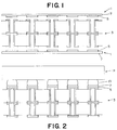
- Figure 1 shows a cross-sectional view of a portion of a multi-layer circuit panel according to the present invention and top and bottom cap 1 according to the present invention prior to attachment to the multi-layer panel 3.
- the electrically conducting material 5 are attached to the panel of an electrically conducting material 7.
- the electrically conducting material 5 forming part of the individual pads are positioned over the plated through holes 9.
- the caps are then attached to the multi-layer structure 3.
- Figure 2 represents a cross-sectional view of an electronic device 11 attached to an embodiment of a cap of the present invention, with the cap attached to a multi-layer circuit panel.
- the device 11 is attached using solder balls 13.
- the cap comprises a plurality of pads.
- Each pad shown in Figure 2 comprises the electrically conducting material 5 and the portion of the panel 7 located above the material 5.
- the pads have also been attached to the side of the multi-layer structure opposite the side that the device is attached to.
- the pads may also include a further portion of electrically conducting material attached to the portion of the panel opposite the electrically conducting material 5.
- a pad is attached over each plated through hole, according to the invention, a pad may not be placed over every through hole.
- a cap structure according to the present invention may be formed by providing a carrier sheet of an electrically conducting material.
- the electrically conducting material may be any known electrically conducting material.
- the electrically conducting material in the panel from which the cap structure is formed and/or the electrically conducting material plated on the panel in the pattern of the ground, power, and/or signal sites of the may be metal such as copper or copper/INVAR/copper, or any other suitable electrically conducting material.
- Further embodiments of methods of the present invention of forming a multi-layer electronic composite may include the step of providing at least one core including a plane of an electrically insulating material having a plane of an electrically insulating material on both sides of the plane of electrically conducting material.
- the at least one core may include a plurality of plated through holes formed therethrough.
- a cap may be formed by providing a panel of a plane of an electrically conducting material including a top surface and a bottom surface.
- a layer of a photosensitive material may be deposited on the top and bottom surface of the electrically conductive plane of the panel. Marks for aligning the cores and the cap may be provided on the cap and/or the cores.
- the photosensitive material on the bottom surface of the electrically conducting plane may be exposed to radiation providing sufficient energy to cause photochemical reactions to occur within the photosensitive material.
- the bottom surface of the cap may be exposed in a pattern matching a pattern of plated through holes formed in the at least one core. All of the photosensitive material on the top surface of the electrically conducting plane of the panel may be exposed to radiation.
- the portions of the photosensitive material not exposed to the radiation may be removed.
- the portions of the electrically conductive layer exposed by removing the portions of the photosensitive material may be cleaned.
- An electrically conducting material may be deposited on the exposed portions of the electrically conducting material.
- the electrically conducting material may be any commonly used material. For instance, gold, gold/tin, or lead/tin solder may be used. All remaining portions of the photosensitive material from the electrically conducting plane may be removed.
- the electrically conducting material deposited on the electrically conducting plane may be aligned with the plated through holes on the core.
- the alignment of the electrically conducting material on the electrically conductive plane with the plated through holes may be verified.
- the panel may be joined to the at least one core by laminating the bottom surface of the panel to the core.
- the top surface of the panel may then be cleaned and a layer of a photosensitive material deposited on the top surface of the panel. Selected portions the photosensitive material on the top surface of the panel may then be exposed to radiation. The radiation preferably causes photochemical reactions to occur within the photosensitive material. The photosensitive material may then be developed to remove portions of the photosensitive material, leaving portions either exposed or not exposed, depending upon the type of photosensitive material used.
- An electrically conducting material may then be deposited on the portions of the surface of the top of the panel uncovered by the removal of the photosensitive material.
- the electrically conducting material forming the base of the panel may then be etched, using the just applied electrically conducting material as a mask.
- One etchant that may be used is ammonium chloride and cupric chloride or an equivalent etchant.
- the etchant will etch the electrically conducting base material and not the just applied electrically conducting material.
- the portions of the photosensitive material deposited on the upper surface of the panel that are not removed during development may be used as a etch mask.
- the panel is etched so as to remove the portions exposed by the removal of the photosensitive material.
- the remaining photosensitive material preferably protects the portions of the panel over the plated through holes. After etching the panel, the remaining photosensitive material may then be removed.
- the electrically conducting material applied where the photosensitive material was removed may be subjected to elevated temperatures to cause any organic plating additives to outgas before attempting to attach a chip or other device.
- the applied electrically conducting material may then be subjected to pressure to flatten or dimple the material. If the photosensitive material is used as an etch mask, then the outgassing step may be deleted and the exposed portion of the panel may be subjected to pressure to flatten or dimple the panel material.
- the pad material prior to flattening, may heated to a temperature sufficient to reflow the material.
- a device such as a semiconductor chip, may be attached to the multi-layer structure at any point after the removal of the material between the pads, whether reflow or mechanical flattening have taken place.
- the top layer of the cap structure described above could by formed from a carrier sheet made of an electrically conducting material.
- the carrier sheet could be made of a metal.
- metals include copper and copper/INVAR/copper
- the sheet may be made from the same material as the electrically conducting plane in the cores of the circuit board.
- Advantages of the present invention include providing a flat surface to facilitate plating of solder to join a chip or other device to a multi-layer structure.
- the flat surface includes discreet conductors surrounded by dielectric material so that a solder mask to prevent undesirable flow of the solder is not required.
- the present invention allows for the attaching of devices without the need for sputtering or plating an electrical commoning layer on the composite panel.
- a multi-layer electronic structure may include at least one core including a plane of an electrically conducting material with a plane of an electrically insulating material on both sides of the plane of electrically conducting material.
- the at least one core includes a plurality of plated through holes formed therethrough.
- a pad or cap is attached over at least one of the plated through holes.
- the pads/caps substantially completely seal the openings of the plated through holes.
- An electronic device including a plurality of ground, signal, and power sites, is attached to the pads/caps. Each of the ground, power, and/or signal sites is attached to one of the pads/caps. If the electronic device is attached to the pads/caps using solder balls, then the composite includes solder balls between the pads/caps and the attached electronic device.
Landscapes
- Engineering & Computer Science (AREA)
- Microelectronics & Electronic Packaging (AREA)
- Physics & Mathematics (AREA)
- Condensed Matter Physics & Semiconductors (AREA)
- General Physics & Mathematics (AREA)
- Computer Hardware Design (AREA)
- Power Engineering (AREA)
- Manufacturing & Machinery (AREA)
- Ceramic Engineering (AREA)
- Combinations Of Printed Boards (AREA)
- Printing Elements For Providing Electric Connections Between Printed Circuits (AREA)
Applications Claiming Priority (2)
| Application Number | Priority Date | Filing Date | Title |
|---|---|---|---|
| US35214494A | 1994-12-01 | 1994-12-01 | |
| US352144 | 1994-12-01 |
Publications (2)
| Publication Number | Publication Date |
|---|---|
| EP0715355A2 true EP0715355A2 (de) | 1996-06-05 |
| EP0715355A3 EP0715355A3 (de) | 1996-12-27 |
Family
ID=23383966
Family Applications (1)
| Application Number | Title | Priority Date | Filing Date |
|---|---|---|---|
| EP95117631A Withdrawn EP0715355A3 (de) | 1994-12-01 | 1995-11-09 | Kappe zum Verschliessen von Vialöchern in LPL |
Country Status (2)
| Country | Link |
|---|---|
| US (4) | US5773195A (de) |
| EP (1) | EP0715355A3 (de) |
Cited By (2)
| Publication number | Priority date | Publication date | Assignee | Title |
|---|---|---|---|---|
| WO2000022894A1 (en) * | 1998-10-13 | 2000-04-20 | Sun Microsystems, Inc. | Apparatus and system with increased signal trace routing options in printed wiring boards and integrated circuit packaging |
| EP3911132A1 (de) * | 2020-05-12 | 2021-11-17 | AT & S Austria Technologie & Systemtechnik Aktiengesellschaft | Bauteilträger mit einem festen körper, der ein bauteilträgerloch vor dem eindringen von fremdkörpern schützt |
Families Citing this family (35)
| Publication number | Priority date | Publication date | Assignee | Title |
|---|---|---|---|---|
| US5773195A (en) * | 1994-12-01 | 1998-06-30 | International Business Machines Corporation | Cap providing flat surface for DCA and solder ball attach and for sealing plated through holes, multi-layer electronic structures including the cap, and a process of forming the cap and for forming multi-layer electronic structures including the cap |
| US5829124A (en) * | 1995-12-29 | 1998-11-03 | International Business Machines Corporation | Method for forming metallized patterns on the top surface of a printed circuit board |
| MY130223A (en) * | 1996-08-27 | 2007-06-29 | Nippon Steel Corp | Semiconductor device provided with low melting point metal bumps and process for producing same |
| US5759737A (en) * | 1996-09-06 | 1998-06-02 | International Business Machines Corporation | Method of making a component carrier |
| JPH1174651A (ja) * | 1997-03-13 | 1999-03-16 | Ibiden Co Ltd | プリント配線板及びその製造方法 |
| US6064116A (en) * | 1997-06-06 | 2000-05-16 | Micron Technology, Inc. | Device for electrically or thermally coupling to the backsides of integrated circuit dice in chip-on-board applications |
| US6076726A (en) | 1998-07-01 | 2000-06-20 | International Business Machines Corporation | Pad-on-via assembly technique |
| US6400028B1 (en) * | 1998-07-20 | 2002-06-04 | Intel Corporation | Alignment of vias in circuit boards or similar structures |
| ES2281188T3 (es) * | 1998-09-10 | 2007-09-16 | Viasystems Group, Inc. | Micro-via no circular. |
| US20020130739A1 (en) * | 1998-09-10 | 2002-09-19 | Cotton Martin A. | Embedded waveguide and embedded electromagnetic shielding |
| US6713685B1 (en) * | 1998-09-10 | 2004-03-30 | Viasystems Group, Inc. | Non-circular micro-via |
| US6514845B1 (en) * | 1998-10-15 | 2003-02-04 | Texas Instruments Incorporated | Solder ball contact and method |
| JP4204150B2 (ja) * | 1998-10-16 | 2009-01-07 | パナソニック株式会社 | 多層回路基板 |
| US6530790B1 (en) * | 1998-11-24 | 2003-03-11 | Teradyne, Inc. | Electrical connector |
| US6846991B2 (en) * | 1999-01-13 | 2005-01-25 | Applied Kinetics, Inc. | Electrical component and a shuntable/shunted electrical component and method for shunting and deshunting |
| US6524164B1 (en) * | 1999-09-14 | 2003-02-25 | Applied Materials, Inc. | Polishing pad with transparent window having reduced window leakage for a chemical mechanical polishing apparatus |
| US6869750B2 (en) * | 1999-10-28 | 2005-03-22 | Fujitsu Limited | Structure and method for forming a multilayered structure |
| US6362438B1 (en) * | 1999-12-15 | 2002-03-26 | Intel Corporation | Enhanced plated-through hole and via contact design |
| US6562641B1 (en) | 2000-08-22 | 2003-05-13 | Micron Technology, Inc. | Apparatus and methods of semiconductor packages having circuit-bearing interconnect components |
| US6504111B2 (en) * | 2001-05-29 | 2003-01-07 | International Business Machines Corporation | Solid via layer to layer interconnect |
| US6660945B2 (en) * | 2001-10-16 | 2003-12-09 | International Business Machines Corporation | Interconnect structure and method of making same |
| US6914334B2 (en) * | 2002-06-12 | 2005-07-05 | Intel Corporation | Circuit board with trace configuration for high-speed digital differential signaling |
| AU2003228259A1 (en) * | 2002-08-08 | 2004-02-25 | Nanoink, Inc. | Protosubstrates |
| US6828512B2 (en) * | 2002-10-08 | 2004-12-07 | Intel Corporation | Apparatus and methods for interconnecting components to via-in-pad interconnects |
| AU2003901146A0 (en) * | 2003-03-12 | 2003-03-27 | Cochlear Limited | Feedthrough assembly |
| US7052288B1 (en) * | 2004-11-12 | 2006-05-30 | Fci Americas Technology, Inc. | Two piece mid-plane |
| US7772115B2 (en) * | 2005-09-01 | 2010-08-10 | Micron Technology, Inc. | Methods for forming through-wafer interconnects, intermediate structures so formed, and devices and systems having at least one solder dam structure |
| WO2009031586A1 (ja) * | 2007-09-06 | 2009-03-12 | Murata Manufacturing Co., Ltd. | 回路基板及び回路基板の製造方法 |
| US10251273B2 (en) * | 2008-09-08 | 2019-04-02 | Intel Corporation | Mainboard assembly including a package overlying a die directly attached to the mainboard |
| KR100968977B1 (ko) * | 2008-10-17 | 2010-07-14 | 삼성전기주식회사 | 무수축 세라믹 기판 및 무수축 세라믹 기판의 제조 방법 |
| US10080287B2 (en) | 2012-09-27 | 2018-09-18 | Dell Products L.P. | Blind via printed circuit board fabrication supporting press fit connectors |
| US9179546B2 (en) * | 2012-09-27 | 2015-11-03 | Dell Products L.P. | Blind via printed circuit board fabrication supporting press fit connectors |
| JP2014192476A (ja) * | 2013-03-28 | 2014-10-06 | Fujitsu Ltd | プリント基板の半田実装方法及び半田実装構造 |
| FR3007403B1 (fr) * | 2013-06-20 | 2016-08-05 | Commissariat Energie Atomique | Procede de realisation d'un dispositif microelectronique mecaniquement autonome |
| US20240047229A1 (en) * | 2022-08-02 | 2024-02-08 | Advanced Micro Devices, Inc. | Organic package core for a substrate with high density plated holes |
Family Cites Families (44)
| Publication number | Priority date | Publication date | Assignee | Title |
|---|---|---|---|---|
| US3509270A (en) * | 1968-04-08 | 1970-04-28 | Ney Co J M | Interconnection for printed circuits and method of making same |
| US3932932A (en) * | 1974-09-16 | 1976-01-20 | International Telephone And Telegraph Corporation | Method of making multilayer printed circuit board |
| DE2724641C2 (de) * | 1977-06-01 | 1986-04-03 | Licentia Patent-Verwaltungs-Gmbh, 6000 Frankfurt | Verfahren zum Aufbringen von Lötungen auf Goldschichten |
| FR2402996A1 (fr) * | 1977-09-12 | 1979-04-06 | Labo Electronique Physique | Procede de realisation de bulles metalliques sur un substrat perce, substrat ainsi traite et utilisation |
| DE2852753C3 (de) * | 1978-12-06 | 1985-06-20 | Württembergische Metallwarenfabrik, 7340 Geislingen | Verfahren zum Befestigen von Bauelementen mit flächigen Anschlußkontakten auf einer Leiterplatte und Schablone zur Durchführung des Verfahrens |
| DE2946726C2 (de) * | 1979-11-20 | 1982-05-19 | Ruwel-Werke Spezialfabrik für Leiterplatten GmbH, 4170 Geldern | Leiterplatte mit starren und flexiblen Bereichen und Verfahren zu deren Herstellung |
| US4468409A (en) * | 1981-09-02 | 1984-08-28 | Chemetron Process Equipment, Inc. | Method for the continuous production of confections |
| US4506443A (en) * | 1982-05-28 | 1985-03-26 | Clarion Co., Ltd. | Method of mounting electric part onto a substrate |
| GB8322473D0 (en) * | 1983-08-20 | 1983-09-21 | Int Computers Ltd | Printed circuit boards |
| GB8333753D0 (en) * | 1983-12-19 | 1984-01-25 | Thorpe J E | Dielectric boards |
| JPS61229389A (ja) * | 1985-04-03 | 1986-10-13 | イビデン株式会社 | セラミツク配線板およびその製造方法 |
| JPS6284973U (de) * | 1985-11-19 | 1987-05-30 | ||
| SU1428534A1 (ru) * | 1986-07-07 | 1988-10-07 | Научно-Исследовательский,Проектно-Конструкторский И Технологический Институт Силовой Полупроводниковой Техники Производственного Объединения "Электровыпрямитель" | Способ пайки электрорадиоэлементов |
| US4788767A (en) * | 1987-03-11 | 1988-12-06 | International Business Machines Corporation | Method for mounting a flexible film semiconductor chip carrier on a circuitized substrate |
| JPS63244631A (ja) * | 1987-03-30 | 1988-10-12 | Nec Corp | 混成集積回路装置の製造方法 |
| US4755911A (en) * | 1987-04-28 | 1988-07-05 | Junkosha Co., Ltd. | Multilayer printed circuit board |
| US4788766A (en) * | 1987-05-20 | 1988-12-06 | Loral Corporation | Method of fabricating a multilayer circuit board assembly |
| JPS6477991A (en) * | 1987-09-18 | 1989-03-23 | Matsushita Electric Industrial Co Ltd | Printed circuit board |
| JPH01102989A (ja) * | 1987-10-16 | 1989-04-20 | Matsushita Electric Ind Co Ltd | ハイブリットic基板 |
| JPH01120891A (ja) * | 1987-11-04 | 1989-05-12 | Nec Corp | 多層プリント配線板 |
| US4864722A (en) * | 1988-03-16 | 1989-09-12 | International Business Machines Corporation | Low dielectric printed circuit boards |
| JPH02283091A (ja) * | 1988-12-20 | 1990-11-20 | Pfu Ltd | プリント板及びその製造方法 |
| JPH02237197A (ja) * | 1989-03-10 | 1990-09-19 | Hitachi Ltd | 多層回路基板及びその製造方法並びにその用途 |
| JPH0798381B2 (ja) * | 1989-05-17 | 1995-10-25 | 旭化成工業株式会社 | 光硬化性樹脂積層体及びそれを用いるプリント配線板の製造方法 |
| JPH03225890A (ja) * | 1990-01-30 | 1991-10-04 | Nec Corp | 印刷配線基板 |
| JPH03262186A (ja) * | 1990-03-13 | 1991-11-21 | Matsushita Electric Ind Co Ltd | 印刷配線基板 |
| US5046238A (en) * | 1990-03-15 | 1991-09-10 | Rogers Corporation | Method of manufacturing a multilayer circuit board |
| US5060844A (en) * | 1990-07-18 | 1991-10-29 | International Business Machines Corporation | Interconnection structure and test method |
| US5243142A (en) * | 1990-08-03 | 1993-09-07 | Hitachi Aic Inc. | Printed wiring board and process for producing the same |
| US5092035A (en) * | 1990-09-10 | 1992-03-03 | Codex Corporation | Method of making printed circuit board assembly |
| US5120678A (en) * | 1990-11-05 | 1992-06-09 | Motorola Inc. | Electrical component package comprising polymer-reinforced solder bump interconnection |
| JP2940269B2 (ja) * | 1990-12-26 | 1999-08-25 | 日本電気株式会社 | 集積回路素子の接続方法 |
| JPH04348595A (ja) * | 1991-05-27 | 1992-12-03 | Hitachi Ltd | 多層印刷回路基板の修復方法 |
| US5200580A (en) * | 1991-08-26 | 1993-04-06 | E-Systems, Inc. | Configurable multi-chip module interconnect |
| US5352926A (en) * | 1993-01-04 | 1994-10-04 | Motorola, Inc. | Flip chip package and method of making |
| US5766670A (en) * | 1993-11-17 | 1998-06-16 | Ibm | Via fill compositions for direct attach of devices and methods for applying same |
| US5275330A (en) * | 1993-04-12 | 1994-01-04 | International Business Machines Corp. | Solder ball connect pad-on-via assembly process |
| US5485038A (en) * | 1993-07-15 | 1996-01-16 | Hughes Aircraft Company | Microelectronic circuit substrate structure including photoimageable epoxy dielectric layers |
| US5773195A (en) * | 1994-12-01 | 1998-06-30 | International Business Machines Corporation | Cap providing flat surface for DCA and solder ball attach and for sealing plated through holes, multi-layer electronic structures including the cap, and a process of forming the cap and for forming multi-layer electronic structures including the cap |
| JP3311899B2 (ja) * | 1995-01-20 | 2002-08-05 | 松下電器産業株式会社 | 回路基板及びその製造方法 |
| US5637920A (en) * | 1995-10-04 | 1997-06-10 | Lsi Logic Corporation | High contact density ball grid array package for flip-chips |
| US5829124A (en) * | 1995-12-29 | 1998-11-03 | International Business Machines Corporation | Method for forming metallized patterns on the top surface of a printed circuit board |
| US5981880A (en) * | 1996-08-20 | 1999-11-09 | International Business Machines Corporation | Electronic device packages having glass free non conductive layers |
| WO1998033366A1 (en) * | 1997-01-29 | 1998-07-30 | Kabushiki Kaisha Toshiba | Method and device for manufacturing multilayered wiring board and wiring board |
-
1995
- 1995-06-07 US US08/480,300 patent/US5773195A/en not_active Expired - Fee Related
- 1995-11-09 EP EP95117631A patent/EP0715355A3/de not_active Withdrawn
-
1996
- 1996-03-20 US US08/619,096 patent/US5734560A/en not_active Expired - Fee Related
-
1998
- 1998-01-05 US US09/003,034 patent/US6098280A/en not_active Expired - Fee Related
-
2000
- 2000-04-28 US US09/559,654 patent/US6594891B1/en not_active Expired - Fee Related
Non-Patent Citations (1)
| Title |
|---|
| None |
Cited By (4)
| Publication number | Priority date | Publication date | Assignee | Title |
|---|---|---|---|---|
| WO2000022894A1 (en) * | 1998-10-13 | 2000-04-20 | Sun Microsystems, Inc. | Apparatus and system with increased signal trace routing options in printed wiring boards and integrated circuit packaging |
| US6534872B1 (en) | 1998-10-13 | 2003-03-18 | Sun Microsystems, Inc. | Apparatus and system with increased signal trace routing options in printed wiring boards and integrated circuit packaging |
| EP3911132A1 (de) * | 2020-05-12 | 2021-11-17 | AT & S Austria Technologie & Systemtechnik Aktiengesellschaft | Bauteilträger mit einem festen körper, der ein bauteilträgerloch vor dem eindringen von fremdkörpern schützt |
| US11612064B2 (en) | 2020-05-12 | 2023-03-21 | AT&SAustria Technologie & Systemtechnik AG | Component carrier with a solid body protecting a component carrier hole from foreign material ingression |
Also Published As
| Publication number | Publication date |
|---|---|
| US5734560A (en) | 1998-03-31 |
| EP0715355A3 (de) | 1996-12-27 |
| US6098280A (en) | 2000-08-08 |
| US5773195A (en) | 1998-06-30 |
| US6594891B1 (en) | 2003-07-22 |
Similar Documents
| Publication | Publication Date | Title |
|---|---|---|
| US5773195A (en) | Cap providing flat surface for DCA and solder ball attach and for sealing plated through holes, multi-layer electronic structures including the cap, and a process of forming the cap and for forming multi-layer electronic structures including the cap | |
| US6066808A (en) | Multilayer circuit board having metallized patterns formed flush with a top surface thereof | |
| US6140707A (en) | Laminated integrated circuit package | |
| US5129142A (en) | Encapsulated circuitized power core alignment and lamination | |
| US5229550A (en) | Encapsulated circuitized power core alignment and lamination | |
| JP3320979B2 (ja) | デバイスをデバイス・キャリヤ上に直接実装する方法 | |
| EP0526133B1 (de) | Mehrschichtige Leiterplatte aus Polyimid und Verfahren zur Herstellung | |
| US6475833B2 (en) | Bumpless flip chip assembly with strips and via-fill | |
| JPH098447A (ja) | チップ実装回路カード構造 | |
| JPH09321408A (ja) | 電子回路基板の高密度実装構造 | |
| JPH08332590A (ja) | 低融点金属キャップを有するリフローはんだボールによる相互接続構造 | |
| US6596620B2 (en) | BGA substrate via structure | |
| JP3577421B2 (ja) | 半導体装置用パッケージ | |
| US6402970B1 (en) | Method of making a support circuit for a semiconductor chip assembly | |
| KR100339252B1 (ko) | 땜납범프(bump)를갖춘반도체장치및그의제조방법 | |
| JPH11111886A (ja) | 実装基板およびその製造方法 | |
| JP3260941B2 (ja) | 多層配線基板および多層配線基板の製造方法 | |
| US6432748B1 (en) | Substrate structure for semiconductor package and manufacturing method thereof | |
| US8546186B2 (en) | Planar interconnect structure for hybrid circuits | |
| JPH11126795A (ja) | 実装基板およびその製造方法ならびに電子部品の実装方法 | |
| US6930383B2 (en) | Electronic component including a housing and a substrate | |
| JP3360492B2 (ja) | 電子回路基板 | |
| JP2002270716A (ja) | 2層配線半導体装置の製造方法および半導体装置 | |
| JPH0888315A (ja) | 電子モジュールおよびその多層化方法 | |
| KR20000032827A (ko) | 다층 회로기판의 접점부 형성방법 |
Legal Events
| Date | Code | Title | Description |
|---|---|---|---|
| PUAI | Public reference made under article 153(3) epc to a published international application that has entered the european phase |
Free format text: ORIGINAL CODE: 0009012 |
|
| AK | Designated contracting states |
Kind code of ref document: A2 Designated state(s): DE FR GB |
|
| PUAL | Search report despatched |
Free format text: ORIGINAL CODE: 0009013 |
|
| 17P | Request for examination filed |
Effective date: 19961029 |
|
| AK | Designated contracting states |
Kind code of ref document: A3 Designated state(s): DE FR GB |
|
| 17Q | First examination report despatched |
Effective date: 19970707 |
|
| STAA | Information on the status of an ep patent application or granted ep patent |
Free format text: STATUS: THE APPLICATION IS DEEMED TO BE WITHDRAWN |
|
| 18D | Application deemed to be withdrawn |
Effective date: 19980403 |