EP0709900A2 - Graben- und Kondensatorstrukturen aus porösem Silizium - Google Patents
Graben- und Kondensatorstrukturen aus porösem Silizium Download PDFInfo
- Publication number
- EP0709900A2 EP0709900A2 EP95480154A EP95480154A EP0709900A2 EP 0709900 A2 EP0709900 A2 EP 0709900A2 EP 95480154 A EP95480154 A EP 95480154A EP 95480154 A EP95480154 A EP 95480154A EP 0709900 A2 EP0709900 A2 EP 0709900A2
- Authority
- EP
- European Patent Office
- Prior art keywords
- silicon
- trench
- layer
- porous silicon
- dielectric material
- Prior art date
- Legal status (The legal status is an assumption and is not a legal conclusion. Google has not performed a legal analysis and makes no representation as to the accuracy of the status listed.)
- Withdrawn
Links
- 239000003990 capacitor Substances 0.000 title claims abstract description 124
- 229910021426 porous silicon Inorganic materials 0.000 title claims abstract description 98
- 238000000034 method Methods 0.000 claims abstract description 33
- 238000005530 etching Methods 0.000 claims abstract description 23
- XUIMIQQOPSSXEZ-UHFFFAOYSA-N Silicon Chemical compound [Si] XUIMIQQOPSSXEZ-UHFFFAOYSA-N 0.000 claims description 107
- 229910052710 silicon Inorganic materials 0.000 claims description 102
- 239000010703 silicon Substances 0.000 claims description 102
- 239000000758 substrate Substances 0.000 claims description 71
- 239000004065 semiconductor Substances 0.000 claims description 61
- 239000003989 dielectric material Substances 0.000 claims description 60
- 150000004767 nitrides Chemical class 0.000 claims description 29
- 229910021420 polycrystalline silicon Inorganic materials 0.000 claims description 25
- 229920005591 polysilicon Polymers 0.000 claims description 19
- 229910021421 monocrystalline silicon Inorganic materials 0.000 claims description 17
- 238000000151 deposition Methods 0.000 claims description 13
- 230000008021 deposition Effects 0.000 claims description 12
- 238000002955 isolation Methods 0.000 claims description 10
- 238000001020 plasma etching Methods 0.000 claims description 6
- 230000015572 biosynthetic process Effects 0.000 claims description 3
- 238000005229 chemical vapour deposition Methods 0.000 claims description 3
- 239000004020 conductor Substances 0.000 claims 1
- 239000012772 electrical insulation material Substances 0.000 claims 1
- 230000003071 parasitic effect Effects 0.000 claims 1
- 239000010410 layer Substances 0.000 description 84
- 210000004027 cell Anatomy 0.000 description 24
- 239000011148 porous material Substances 0.000 description 11
- KRHYYFGTRYWZRS-UHFFFAOYSA-N Fluorane Chemical compound F KRHYYFGTRYWZRS-UHFFFAOYSA-N 0.000 description 8
- 238000009792 diffusion process Methods 0.000 description 5
- 238000002048 anodisation reaction Methods 0.000 description 4
- 238000005516 engineering process Methods 0.000 description 4
- 238000009413 insulation Methods 0.000 description 4
- 239000002356 single layer Substances 0.000 description 4
- 229910052581 Si3N4 Inorganic materials 0.000 description 3
- 238000010276 construction Methods 0.000 description 3
- 230000000873 masking effect Effects 0.000 description 3
- HQVNEWCFYHHQES-UHFFFAOYSA-N silicon nitride Chemical compound N12[Si]34N5[Si]62N3[Si]51N64 HQVNEWCFYHHQES-UHFFFAOYSA-N 0.000 description 3
- 238000003860 storage Methods 0.000 description 3
- 238000007743 anodising Methods 0.000 description 2
- 239000011248 coating agent Substances 0.000 description 2
- 238000000576 coating method Methods 0.000 description 2
- 239000002019 doping agent Substances 0.000 description 2
- 239000008151 electrolyte solution Substances 0.000 description 2
- 230000010354 integration Effects 0.000 description 2
- 239000000463 material Substances 0.000 description 2
- BASFCYQUMIYNBI-UHFFFAOYSA-N platinum Chemical compound [Pt] BASFCYQUMIYNBI-UHFFFAOYSA-N 0.000 description 2
- 239000000243 solution Substances 0.000 description 2
- 125000006850 spacer group Chemical group 0.000 description 2
- ZOXJGFHDIHLPTG-UHFFFAOYSA-N Boron Chemical compound [B] ZOXJGFHDIHLPTG-UHFFFAOYSA-N 0.000 description 1
- OAICVXFJPJFONN-UHFFFAOYSA-N Phosphorus Chemical compound [P] OAICVXFJPJFONN-UHFFFAOYSA-N 0.000 description 1
- 229910052785 arsenic Inorganic materials 0.000 description 1
- RQNWIZPPADIBDY-UHFFFAOYSA-N arsenic atom Chemical compound [As] RQNWIZPPADIBDY-UHFFFAOYSA-N 0.000 description 1
- 229910052796 boron Inorganic materials 0.000 description 1
- 238000006243 chemical reaction Methods 0.000 description 1
- 230000002860 competitive effect Effects 0.000 description 1
- 239000002131 composite material Substances 0.000 description 1
- 230000009977 dual effect Effects 0.000 description 1
- 230000005669 field effect Effects 0.000 description 1
- 238000004519 manufacturing process Methods 0.000 description 1
- 230000001590 oxidative effect Effects 0.000 description 1
- 229910052698 phosphorus Inorganic materials 0.000 description 1
- 239000011574 phosphorus Substances 0.000 description 1
- 229910052697 platinum Inorganic materials 0.000 description 1
- 238000004886 process control Methods 0.000 description 1
- 230000004580 weight loss Effects 0.000 description 1
Images


Classifications
-
- H—ELECTRICITY
- H01—ELECTRIC ELEMENTS
- H01L—SEMICONDUCTOR DEVICES NOT COVERED BY CLASS H10
- H01L29/00—Semiconductor devices adapted for rectifying, amplifying, oscillating or switching, or capacitors or resistors with at least one potential-jump barrier or surface barrier, e.g. PN junction depletion layer or carrier concentration layer; Details of semiconductor bodies or of electrodes thereof ; Multistep manufacturing processes therefor
-
- H—ELECTRICITY
- H01—ELECTRIC ELEMENTS
- H01L—SEMICONDUCTOR DEVICES NOT COVERED BY CLASS H10
- H01L28/00—Passive two-terminal components without a potential-jump or surface barrier for integrated circuits; Details thereof; Multistep manufacturing processes therefor
- H01L28/40—Capacitors
- H01L28/60—Electrodes
- H01L28/82—Electrodes with an enlarged surface, e.g. formed by texturisation
-
- H—ELECTRICITY
- H01—ELECTRIC ELEMENTS
- H01L—SEMICONDUCTOR DEVICES NOT COVERED BY CLASS H10
- H01L29/00—Semiconductor devices adapted for rectifying, amplifying, oscillating or switching, or capacitors or resistors with at least one potential-jump barrier or surface barrier, e.g. PN junction depletion layer or carrier concentration layer; Details of semiconductor bodies or of electrodes thereof ; Multistep manufacturing processes therefor
- H01L29/66—Types of semiconductor device ; Multistep manufacturing processes therefor
- H01L29/66007—Multistep manufacturing processes
- H01L29/66075—Multistep manufacturing processes of devices having semiconductor bodies comprising group 14 or group 13/15 materials
- H01L29/66083—Multistep manufacturing processes of devices having semiconductor bodies comprising group 14 or group 13/15 materials the devices being controllable only by variation of the electric current supplied or the electric potential applied, to one or more of the electrodes carrying the current to be rectified, amplified, oscillated or switched, e.g. two-terminal devices
- H01L29/66181—Conductor-insulator-semiconductor capacitors, e.g. trench capacitors
-
- H—ELECTRICITY
- H01—ELECTRIC ELEMENTS
- H01L—SEMICONDUCTOR DEVICES NOT COVERED BY CLASS H10
- H01L29/00—Semiconductor devices adapted for rectifying, amplifying, oscillating or switching, or capacitors or resistors with at least one potential-jump barrier or surface barrier, e.g. PN junction depletion layer or carrier concentration layer; Details of semiconductor bodies or of electrodes thereof ; Multistep manufacturing processes therefor
- H01L29/66—Types of semiconductor device ; Multistep manufacturing processes therefor
- H01L29/86—Types of semiconductor device ; Multistep manufacturing processes therefor controllable only by variation of the electric current supplied, or only the electric potential applied, to one or more of the electrodes carrying the current to be rectified, amplified, oscillated or switched
- H01L29/92—Capacitors with potential-jump barrier or surface barrier
- H01L29/94—Metal-insulator-semiconductors, e.g. MOS
- H01L29/945—Trench capacitors
-
- H—ELECTRICITY
- H10—SEMICONDUCTOR DEVICES; ELECTRIC SOLID-STATE DEVICES NOT OTHERWISE PROVIDED FOR
- H10B—ELECTRONIC MEMORY DEVICES
- H10B12/00—Dynamic random access memory [DRAM] devices
- H10B12/01—Manufacture or treatment
- H10B12/02—Manufacture or treatment for one transistor one-capacitor [1T-1C] memory cells
- H10B12/03—Making the capacitor or connections thereto
- H10B12/038—Making the capacitor or connections thereto the capacitor being in a trench in the substrate
-
- Y—GENERAL TAGGING OF NEW TECHNOLOGICAL DEVELOPMENTS; GENERAL TAGGING OF CROSS-SECTIONAL TECHNOLOGIES SPANNING OVER SEVERAL SECTIONS OF THE IPC; TECHNICAL SUBJECTS COVERED BY FORMER USPC CROSS-REFERENCE ART COLLECTIONS [XRACs] AND DIGESTS
- Y10—TECHNICAL SUBJECTS COVERED BY FORMER USPC
- Y10S—TECHNICAL SUBJECTS COVERED BY FORMER USPC CROSS-REFERENCE ART COLLECTIONS [XRACs] AND DIGESTS
- Y10S438/00—Semiconductor device manufacturing: process
- Y10S438/96—Porous semiconductor
-
- Y—GENERAL TAGGING OF NEW TECHNOLOGICAL DEVELOPMENTS; GENERAL TAGGING OF CROSS-SECTIONAL TECHNOLOGIES SPANNING OVER SEVERAL SECTIONS OF THE IPC; TECHNICAL SUBJECTS COVERED BY FORMER USPC CROSS-REFERENCE ART COLLECTIONS [XRACs] AND DIGESTS
- Y10—TECHNICAL SUBJECTS COVERED BY FORMER USPC
- Y10S—TECHNICAL SUBJECTS COVERED BY FORMER USPC CROSS-REFERENCE ART COLLECTIONS [XRACs] AND DIGESTS
- Y10S977/00—Nanotechnology
- Y10S977/70—Nanostructure
- Y10S977/701—Integrated with dissimilar structures on a common substrate
- Y10S977/72—On an electrically conducting, semi-conducting, or semi-insulating substrate
- Y10S977/721—On a silicon substrate
-
- Y—GENERAL TAGGING OF NEW TECHNOLOGICAL DEVELOPMENTS; GENERAL TAGGING OF CROSS-SECTIONAL TECHNOLOGIES SPANNING OVER SEVERAL SECTIONS OF THE IPC; TECHNICAL SUBJECTS COVERED BY FORMER USPC CROSS-REFERENCE ART COLLECTIONS [XRACs] AND DIGESTS
- Y10—TECHNICAL SUBJECTS COVERED BY FORMER USPC
- Y10S—TECHNICAL SUBJECTS COVERED BY FORMER USPC CROSS-REFERENCE ART COLLECTIONS [XRACs] AND DIGESTS
- Y10S977/00—Nanotechnology
- Y10S977/84—Manufacture, treatment, or detection of nanostructure
- Y10S977/888—Shaping or removal of materials, e.g. etching
-
- Y—GENERAL TAGGING OF NEW TECHNOLOGICAL DEVELOPMENTS; GENERAL TAGGING OF CROSS-SECTIONAL TECHNOLOGIES SPANNING OVER SEVERAL SECTIONS OF THE IPC; TECHNICAL SUBJECTS COVERED BY FORMER USPC CROSS-REFERENCE ART COLLECTIONS [XRACs] AND DIGESTS
- Y10—TECHNICAL SUBJECTS COVERED BY FORMER USPC
- Y10S—TECHNICAL SUBJECTS COVERED BY FORMER USPC CROSS-REFERENCE ART COLLECTIONS [XRACs] AND DIGESTS
- Y10S977/00—Nanotechnology
- Y10S977/84—Manufacture, treatment, or detection of nanostructure
- Y10S977/895—Manufacture, treatment, or detection of nanostructure having step or means utilizing chemical property
- Y10S977/896—Chemical synthesis, e.g. chemical bonding or breaking
- Y10S977/899—Electrolytic
Definitions
- This invention relates to high surface area capacitors for use in the semiconductor industry, and more particularly to capacitors utilizing porous silicon as one plate of the capacitor to increase the surface area thereof.
- VLSI Very Large Scale Integration
- ULSI Ultra Large Scale Integration
- a two-dimensional design capacitor includes a planar capacitor (see Fig. 1).
- the lower plate of the capacitor is formed from the n+ silicon substrate extension 12 of storage node junction 14 of field - effect transistor (FET) 15.
- the upper capacitor plate (or field plate) 16 is formed from a layer of conductively-doped polycrystalline silicon.
- Node extension 12 is electrically insulated from upper plate 16 by a dielectric layer 18.
- Planar capacitors have generally proven adequate for use in DRAM chips up to the one-megabit level.
- the desirable size of capacitors has grown smaller and smaller while the desirable capacitance has increased.
- the difficult goal of a DRAM designer is therefore to increase, or at least maintain, cell capacitance as cell size shrinks, without resorting to processes that reduce product yield or that markedly increase the number of masking and deposition steps in the production process.
- Such three-dimensional capacitors include trench capacitors and stacked capacitors.
- Trench capacitors 19 are employed to provide greater plate area, and therefore greater capacitance.
- the lower plate 20 may be formed from the n+ doped silicon substrate or it may be formed from a polysilicon layer which lines a trench cut in the n+ doped silicon substrate.
- the upper plate 22 is formed from a layer of conductively-doped polycrystalline silicon. Lower plate 20 and upper plate 22 are electrically insulated with a dielectric layer 24.
- FIG. 3 is a graphic representation of a typical DRAM cell having a stacked capacitor 26.
- the lower plate 28 is formed from an n-type polycrystalline silicon layer which is in contact with the silicon substrate 30 in the region of the FET storage node junction, while the upper plate 32 is formed from a conductively-doped polycrystalline silicon layer. The two layers are separated by a dielectric layer 34.
- Lower plate 28 and upper plate 32 are both stacked on top of FET 36 and word line 38, resulting in a high-profile cell which requires more stringent process control for the connection of bit line 40 to access-node junction 42.
- the deposited and anodized layer of porous silicon forms the first plate of a capacitor, which due to its porous nature has a greater surface area for capacitance.
- One or more of the Sandhu patents disclose a single layer of silicon nitride as the suitable thin layer dielectric for use in DRAMs where capacitative layers are not smooth (i.e. porous silicon) as well as the use of polycrystalline silicon lined trench designs. This severely limits the applicability of the structure and method disclosed in Sandhu since multi-layer dielectrics such as oxide/nitride, nitride/oxide, and oxide/nitride/oxide dielectrics offer significant advantages over single layer silicon nitride in many applications.
- the subject invention utilizes the anodic etching of silicon, such as p+ monocrystalline silicon, to form pores or depressions in the silicon.
- silicon such as p+ monocrystalline silicon
- the dielectric material extends to within the porous structure, coating substantially the entire surface of the pores within the porous silicon (referred to herein as conformally overlying the porous silicon).
- a layer of silicon is then deposited overlying the dielectric material, which again extends to within the porous structure, coating substantially the entire surface of the dielectric material within the pores within the porous silicon (referred to herein as conformally overlying the dielectric material).
- the resulting structure has a surface area for the capacitor (comprising the porous silicon as a first plate, the layer of silicon as the second plate, and the dielectric layer separating the first and second plates) much greater than can be achieved without making the silicon porous.
- the invention will be more readily understood in the context of the examples which follow.
- one embodiment of the present invention is directed to a semiconductor capacitor structure comprising a semiconductor substrate of silicon having an area of porous silicon extending into the substrate, a conformal layer of a dielectric material overlying the semiconductor substrate at the area of porous silicon, and a conformal layer of silicon overlying the layer of dielectric material.
- the area of porous silicon thus forms a first plate of a capacitor, and the conformal layer of silicon forms the second plate of the capacitor.
- the first plate and the second plate are separated by the dielectric material, which is preferably a multi-layer dielectric such as oxide/nitride, nitride/oxide, or oxide/nitride/oxide.
- Multi-layer dielectrics are preferred over single layer dielectrics because they are generally less conductive and therefore are better dielectrics for storing charge for a long period of time. Furthermore, multi-layer dielectrics are less likely than single layer silicon nitride dielectrics to trap charge because they are less conductive. It is undesirable for a dielectric in a storage capacitor to trap charge because then the amount of charge that can be stored in the capacitor will vary with time.
- the semiconductor substrate can be monocrystalline silicon, and is preferably p+ monocrystalline silicon, and the conformal layer of silicon is preferably polysilicon.
- the area of porous silicon is preferably formed by electrolytic anodic etching.
- a semiconductor trench structure which can be utilized in capacitor formation.
- the trench is formed in a semiconductor substrate, which may have an upper portion of p- or n-doped silicon and a lower portion of p+ silicon, in which case the trench is formed through the upper portion and into the lower portion.
- a porous silicon region surrounds the side walls and bottom of the trench. The location of the porous silicon region is determined by the selectivity of the anodic etch used to form the porous silicon. In one example, anodic etching is selective for the p+ silicon lower portion and therefore the porous silicon region does not extend appreciably into the p- or n-doped upper portion of silicon.
- the silicon substrate is preferably monocrystalline silicon.
- the trench structure is utilized to form a capacitor structure by including a conformal layer of a dielectric material overlying the porous silicon region, and a conformal layer of silicon overlying the layer of dielectric.
- the porous silicon region thus forms the first plate of a capacitor structure, with the layer of silicon forming the second plate of the capacitor structure.
- the first plate and second plate are separated by the dielectric layer.
- Suitable dielectric layers in this embodiment can also include oxide or nitride in addition to multi-layer dielectrics such as oxide/nitride, nitride/oxide, and oxide/nitride/oxide, although multi-layer dielectrics are preferred, and the conformal silicon layer again preferably comprises polysilicon.
- the anodic etching of the silicon to form porous silicon is utilized to form isolated, adjacent trenches.
- a trench structure which comprises a semiconductor substrate of silicon, which may have an upper portion of p- or n-doped silicon and a lower portion of p+ silicon.
- a first trench is formed in the semiconductor substrate, such as through the upper portion and into the lower portion, and the silicon in the lower portion surrounding the trench is made porous through anodic etching.
- a second trench is formed in the semiconductor substrate, such as through the upper portion and into the lower portion. The second trench is adjacent to the first trench, and must be isolated therefrom for proper functioning of the semiconductor device.
- This isolation is achieved through the electrolytic anodic etching of the porous silicon regions surrounding each of the two adjacent trenches.
- the anodic etching is self-limiting and leaves a wisp or continuous area of non-porous silicon in the semiconductor substrate between the two porous silicon regions.
- the anodic etching and creation of the wisp or continuous area of non-porous silicon is described in Tsao et al. J. Appl. Phys. Vol. 62, No. 10, 15 Nov 1987, which is hereby incorporated by reference.
- the wisp is formed in the p+ silicon of the lower portion of the substrate.
- this trench structure can be utilized to form a capacitor structure by the deposition of a conformal layer of a dielectric material overlying the porous silicon regions, and then conformally depositing a layer of silicon overlying the dielectric material.
- Two capacitor structures are thus formed.
- the first comprises the porous silicon area surrounding the first trench, the dielectric deposited thereover, and the layer of silicon deposited thereover.
- the second capacitor comprises the porous silicon area surrounding the second trench, the dielectric deposited thereover, and the layer of silicon deposited thereover.
- Suitable semiconductor substrates, dielectric materials, and layers of silicon are as described in the previous examples of trench/capacitor structures.
- the principles of the subject invention can be applied to various trench technologies, including semiconductor trench capacitor cells with merged isolation and node trench construction (see U.S. Patent No. 4,801,988).
- the surface area of the trench capacitor is increased by utilizing porous silicon as the first plate of the capacitor structure, in which the isolation layer and node trench are merged such that the isolation regions are self-aligned to the trench side walls.
- a trench capacitor of this type even without the porous silicon usage, provides for greater surface area within a given space due to the merger. By utilizing porous silicon, this increase in surface area for the capacitor is even greater.
- the broad concept of the subject invention is directed to the use of porous silicon as a first plate of a capacitor structure, thereby greatly increasing the surface area available for the capacitor and thereby the capacitance attainable.
- This concept can be utilized with many types of capacitors, including planar, trench, and stacked capacitors.
- Porous silicon is produced utilizing anodic etching.
- Anodic etching is performed by submerging the silicon wafer or other silicon substrate in a container of electrolytic solution of hydrofluoric acid and subjecting the wafer to an electrolytic current.
- the electrolytic current is generated between two electrodes, an anode and a cathode.
- the wafer or other silicon substrate comprises the anode.
- the container, or a platinum electrode immersed in the electrolytic solution parallel to the wafer or substrate, comprises the cathode.
- anodizing creates a porous surface on the material employed as the anode.
- the resulting microstructure of the porous surface is a series of elongated pores or depressions, formed by the anodic conversion of the silicon in the hydrofluoric acid.
- Anodization is typically conducted with a current density range of 10 mA/cm to 100 mA/cm in a hydrofluoric acid solution having a concentration range between 10 and 60 percent by weight.
- the anodization current and concentration of hydrofluoric acid solution are typically chosen to produce a porous film density of substantially 45 percent. Porous film density is equal to the percent of weight loss (for a given volume of material anodized) experienced during anodization.
- P- doped silicon is lightly doped p silicon, and p+ doped silicon is heavily doped p silicon.
- Suitable p-type dopants are known in the art, and include boron.
- N-type dopants to form n-doped silicon are also known in the art and include, for example, arsenic or phosphorus.
- the silicon substrate may be a silicon wafer, typically comprising a p+ silicon substrate with a p- epitaxial layer on its surface.
- the formation of conformal overlying layers of dielectric material and silicon can be by any suitable means. Chemical vapor deposition is preferred because this process is capable of deposition within the microstructure of the porous silicon.
- the dielectric can also be formed by partially oxidizing or nitridizing the silicon substrate, partially filling the microstructure pores or depressions. Each and every pore or depression does not need to be filled with the dielectric and silicon layers. A small amount of unfilled pores will slightly decrease the great increase in surface area attained with the porous silicon as the plate of the capacitor.
- Preferred thickness of the dielectric material is as follows: oxide, less than nm; nitride, less than nm; oxide/nitride, less than nm of oxide and less than nm of nitride; nitride/oxide, less than nm of nitride and less than nm of oxide; oxide/nitride/oxide, less than nm of the first oxide, less than nm of the nitride, and less than nm of the second oxide.
- a silicon substrate 44 is shown.
- the silicon substrate 44 is anodically etched to form a porous silicon region 46 (see FIG. 5).
- the porous silicon region as used throughout this application refers to a microstructure such as that as shown in FIG. 7 having a series of random pores or depressions throughout the porous silicon region.
- a conformal layer of dielectric material 48 is formed overlying the porous silicon region 46, followed by a conformal layer of polysilicon 50 (see FIG. 6).
- the conformal layer of dielectric material overlying the porous silicon region refers to the dielectric material extending to within the porous microstructure.
- the conformal layer of polysilicon overlying the dielectric material also extends to within the porous microstructure.
- the capacitor structure is thus comprised of the first plate of porous silicon 46, the second plate of polysilicon 50, and the dielectric material 48 separating the two plates.
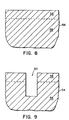
- a silicon substrate 54 has an upper portion 56 of p- silicon and a lower portion 58 of p+ silicon.
- a trench 60 is etched into the silicon substrate 54, through the upper portion 56 and into the lower portion 58 (see FIG. 9).
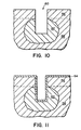
- Anodic etching is then utilized to form a porous silicon region 62 surrounding the trench sidewalls and the trench bottom in the lower portion 58 of the silicon substrate.
- Porous silicon forms much more rapidly in the P+ silicon than in the P- silicon therefore generally resulting in a structure depicted in FIG. 10.
- This porous silicon region 62 forms the first plate of a capacitor structure, onto which is conformally deposited an overlying layer of dielectric material 64 (see FIG. 11) followed by conformal deposition of an overlying polysilicon layer 66 (see FIG. 12). As shown in the enlargement 68 of FIG. 13, the porous silicon region 62 thus forms the first plate of the capacitor which is separated from the second plate of the capacitor, the polysilicon 66, by the dielectric material 64.
- a self-limiting method is provided according to the subject invention to form isolated, adjacent trenches.
- a silicon substrate 70 is again shown as having an upper portion 72 of p- silicon and a lower portion 74 of p+ silicon.
- Two adjacent trenches 76 and 78 are reactive ion etched into the silicon substrate 70, through the upper portion 72 and into the lower portion 74 (see FIG. 15).
- Anodic etching is utilized to form a porous silicon region 80 surrounding the lower portion of trench 76, and to form a porous silicon region 82 surrounding the lower portion of trench 78.
- the anodic etching process is self-limiting, in that the two areas of porous silicon 80 and 82 will not connect.
- a wisp or layer of non-porous silicon 84 will remain between the two porous silicon regions, keeping trench 76 isolated from trench 78 (see FIG. 16).
- a conformal overlying layer of dielectric material 86 is deposited (see FIG. 17), followed by a conformal overlying layer of polysilicon 88 (see FIG. 18).
- the resulting capacitor structures utilize the porous silicon region 80 or 82 as the first plate of a capacitor structure, with the dielectric material 86 separating the first plate from the second plate of polysilicon 88.
- the separate porous silicon regions are self-aligned to their respective cells to utilize a high percentage of cell area for the capacitors.
- MINT merged isolation and node trench
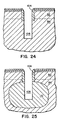
- a semiconductor substrate of silicon 90 is shown with p- upper portion 92 and p+ lower portion 94.
- Masking films of oxide 96 and nitride 98 are utilized to define a trench (see FIG. 20), and the trench 100 is then etched into the silicon substrate 90 through the upper portion 92 and into the lower portion 94 (see FIG. 21) to a first trench depth.
- a layer of dielectric material 102 such as a dual oxide and nitride layer, is then conformally deposited (see FIG. 22).
- Reactive ion etching (RIE) is then utilized to etch away the dielectric material on all horizontal surfaces, leaving the vertical sidewall spacers 104 shown in FIG. 23 and the exposed horizontal surfaces 106. Further RIE is then utilized to etch a deeper trench 108 into the p+ lower portion 94 of the silicon substrate (see FIG. 24).
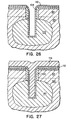
- the concept of the subject invention is utilized to increase the surface area that will be available for the capacitor structure. This is accomplished by utilizing anodic etching to form a porous silicon region 110 surrounding the trench 108 sidewalls and bottom in the p+ portion 94 of the silicon substrate (see FIG. 25). Note that the porous silicon region 110 does not extend appreciably above the level of the sidewall spacers 104 into the p- portion 92.
- a conformal overlying layer of dielectric 112 is then deposited (see FIG. 26) followed by a conformal overlying layer of polysilicon 114 (see FIG. 27) which forms the second plate of the capacitor.
- the first plate is separated from the second plate by the dielectric material 112.
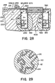
- FIG. 28 shows the MINT capacitor structure of FIG. 27 as it may be incorporated into a semiconductor device.
- a dynamic memory cell with a semiconductor trench capacitor cell structure according to one embodiment of the subject invention is shown.
- the dynamic memory cell is formed in a composite semiconductor substrate 210 in which an N-well 230 is formed in a P+ substrate portion 220.
- a transistor is constructed of a P+ drain diffusion 250, a gate electrode 260, and a P+ source diffusion 270.
- the insulation between the gate electrode 260 and the substrate as well as the thin insulating layer on top of the source diffusion 270 and drain diffusion 250 is shown schematically as a single thin insulation layer 215.
- a partial section of a recessed oxide layer 299 which can be used to support and insulate additional memory array circuitry (e.g. wordlines and bitlines, not shown).
- Adjacent to the source diffusion 270 is a semiconductor trench capacitor cell 240 of one embodiment of the subject invention.
- the semiconductor trench capacitor cell 240 is insulated from the semiconductor substrate 210 by a thin insulation layer 290, and is isolated from adjacent semiconductor trench capacitor cells by side-wall defined, thick isolation layers 340 and 350.
- another semiconductor trench capacitor cell 310 is also insulated from the semiconductor substrate 210 by a thin insulation layer 330, and is isolated from adjacent devices by thick isolation layers 380 and 390.
- Both semiconductor trench capacitor cells are filled with a P+ doped conductive polysilicon 280 and 320 respectively.
- each trench capacitor cell 240 and 310 is surrounded by an area of porous silicon, 410 and 420 respectively, separated by a wisp or area of non-porous silicon 430.
- the great increase in surface area according to the structures and methods of the subject invention is best illustrated in the enlargement 52 shown in FIG. 29.
- the structure on a microscopic level is actually a series of random pores or depressions in the silicon forming the porous silicon 46.
- the conformal overlying layer of the dielectric material 48 extends to within each of the pores or depressions within the porous silicon 46 as shown.
- the conformal overlying layer of the polysilicon 50 likewise extends to within each of the pores or depressions, resulting in a capacitor structure such as is shown in FIG. 29 which utilizes the entire surface area of the porous silicon for the capacitor plate.
Applications Claiming Priority (2)
| Application Number | Priority Date | Filing Date | Title |
|---|---|---|---|
| US330652 | 1994-10-28 | ||
| US08/330,652 US5508542A (en) | 1994-10-28 | 1994-10-28 | Porous silicon trench and capacitor structures |
Publications (2)
| Publication Number | Publication Date |
|---|---|
| EP0709900A2 true EP0709900A2 (de) | 1996-05-01 |
| EP0709900A3 EP0709900A3 (de) | 1996-08-07 |
Family
ID=23290697
Family Applications (1)
| Application Number | Title | Priority Date | Filing Date |
|---|---|---|---|
| EP95480154A Withdrawn EP0709900A3 (de) | 1994-10-28 | 1995-10-03 | Graben- und Kondensatorstrukturen aus porösem Silizium |
Country Status (4)
| Country | Link |
|---|---|
| US (2) | US5508542A (de) |
| EP (1) | EP0709900A3 (de) |
| JP (1) | JP3079021B2 (de) |
| KR (1) | KR100192186B1 (de) |
Cited By (4)
| Publication number | Priority date | Publication date | Assignee | Title |
|---|---|---|---|---|
| WO1998032166A1 (de) * | 1997-01-21 | 1998-07-23 | Siemens Aktiengesellschaft | Verfahren zur herstellung eines siliziumkondensators |
| DE10030696A1 (de) * | 2000-06-23 | 2002-01-10 | Infineon Technologies Ag | Integrierte Schaltungsanordnung mit zumindest einem vergrabenen Schaltungselement und einer Isolationsschicht sowie Verfahren zu deren Herstellung |
| DE102010013492A1 (de) * | 2010-03-31 | 2011-10-06 | Arne-Christian Voigt | Nanostrukturkondensator |
| EP2939250A4 (de) * | 2012-12-28 | 2016-10-05 | Intel Corp | Mit porösem silicium geformte energiespeichervorrichtungen |
Families Citing this family (85)
| Publication number | Priority date | Publication date | Assignee | Title |
|---|---|---|---|---|
| JPH08148280A (ja) * | 1994-04-14 | 1996-06-07 | Toshiba Corp | 半導体装置およびその製造方法 |
| US5731235A (en) * | 1996-10-30 | 1998-03-24 | Micron Technology, Inc. | Methods of forming a silicon nitrite film, a capacitor dielectric layer and a capacitor |
| US5877061A (en) * | 1997-02-25 | 1999-03-02 | International Business Machines Corporation | Methods for roughening and volume expansion of trench sidewalls to form high capacitance trench cell for high density dram applications |
| US7067406B2 (en) * | 1997-03-31 | 2006-06-27 | Intel Corporation | Thermal conducting trench in a semiconductor structure and method for forming the same |
| US6222254B1 (en) * | 1997-03-31 | 2001-04-24 | Intel Corporation | Thermal conducting trench in a semiconductor structure and method for forming the same |
| US5767561A (en) * | 1997-05-09 | 1998-06-16 | Lucent Technologies Inc. | Integrated circuit device with isolated circuit elements |
| US6188097B1 (en) | 1997-07-02 | 2001-02-13 | Micron Technology, Inc. | Rough electrode (high surface area) from Ti and TiN |
| US6072209A (en) | 1997-07-08 | 2000-06-06 | Micro Technology, Inc. | Four F2 folded bit line DRAM cell structure having buried bit and word lines |
| US6150687A (en) | 1997-07-08 | 2000-11-21 | Micron Technology, Inc. | Memory cell having a vertical transistor with buried source/drain and dual gates |
| US6191470B1 (en) | 1997-07-08 | 2001-02-20 | Micron Technology, Inc. | Semiconductor-on-insulator memory cell with buried word and body lines |
| US5936274A (en) * | 1997-07-08 | 1999-08-10 | Micron Technology, Inc. | High density flash memory |
| US5973356A (en) * | 1997-07-08 | 1999-10-26 | Micron Technology, Inc. | Ultra high density flash memory |
| US5909618A (en) | 1997-07-08 | 1999-06-01 | Micron Technology, Inc. | Method of making memory cell with vertical transistor and buried word and body lines |
| EP0903782A3 (de) * | 1997-09-19 | 2001-10-10 | Siemens Aktiengesellschaft | DRAM Grabenkondensator mit vergrösserter Oberfläche |
| US5907170A (en) * | 1997-10-06 | 1999-05-25 | Micron Technology, Inc. | Circuit and method for an open bit line memory cell with a vertical transistor and trench plate trench capacitor |
| US6528837B2 (en) * | 1997-10-06 | 2003-03-04 | Micron Technology, Inc. | Circuit and method for an open bit line memory cell with a vertical transistor and trench plate trench capacitor |
| US6066869A (en) | 1997-10-06 | 2000-05-23 | Micron Technology, Inc. | Circuit and method for a folded bit line memory cell with vertical transistor and trench capacitor |
| US5914511A (en) * | 1997-10-06 | 1999-06-22 | Micron Technology, Inc. | Circuit and method for a folded bit line memory using trench plate capacitor cells with body bias contacts |
| US6063713A (en) * | 1997-11-10 | 2000-05-16 | Micron Technology, Inc. | Methods for forming silicon nitride layers on silicon-comprising substrates |
| EP1048082A1 (de) * | 1997-11-12 | 2000-11-02 | Epcos Ag | Schaltungsstruktur mit mindestens einem kondensator und verfahren zu dessen herstellung |
| US6025225A (en) * | 1998-01-22 | 2000-02-15 | Micron Technology, Inc. | Circuits with a trench capacitor having micro-roughened semiconductor surfaces and methods for forming the same |
| US5963469A (en) * | 1998-02-24 | 1999-10-05 | Micron Technology, Inc. | Vertical bipolar read access for low voltage memory cell |
| US6304483B1 (en) | 1998-02-24 | 2001-10-16 | Micron Technology, Inc. | Circuits and methods for a static random access memory using vertical transistors |
| US6242775B1 (en) | 1998-02-24 | 2001-06-05 | Micron Technology, Inc. | Circuits and methods using vertical complementary transistors |
| US6246083B1 (en) | 1998-02-24 | 2001-06-12 | Micron Technology, Inc. | Vertical gain cell and array for a dynamic random access memory |
| US6124729A (en) | 1998-02-27 | 2000-09-26 | Micron Technology, Inc. | Field programmable logic arrays with vertical transistors |
| US5991225A (en) | 1998-02-27 | 1999-11-23 | Micron Technology, Inc. | Programmable memory address decode array with vertical transistors |
| US6043527A (en) * | 1998-04-14 | 2000-03-28 | Micron Technology, Inc. | Circuits and methods for a memory cell with a trench plate trench capacitor and a vertical bipolar read device |
| EP1092234A1 (de) | 1998-06-05 | 2001-04-18 | Georgia Tech Research | Poröse, isolierende verbindung und dessen herstellung |
| US6093623A (en) | 1998-08-04 | 2000-07-25 | Micron Technology, Inc. | Methods for making silicon-on-insulator structures |
| US6134175A (en) * | 1998-08-04 | 2000-10-17 | Micron Technology, Inc. | Memory address decode array with vertical transistors |
| US6208164B1 (en) | 1998-08-04 | 2001-03-27 | Micron Technology, Inc. | Programmable logic array with vertical transistors |
| US6762057B1 (en) * | 1998-10-23 | 2004-07-13 | Micron Technology, Inc. | Separation apparatus including porous silicon column |
| US7115422B1 (en) * | 1998-10-23 | 2006-10-03 | Micron Technology, Inc. | Separation apparatus including porous silicon column |
| US6423613B1 (en) | 1998-11-10 | 2002-07-23 | Micron Technology, Inc. | Low temperature silicon wafer bond process with bulk material bond strength |
| CN1349670A (zh) * | 1999-05-06 | 2002-05-15 | 三帝公司 | 燃料电池和薄膜 |
| US6890677B2 (en) | 1999-05-06 | 2005-05-10 | Sandia Corporation | Fuel cell and membrane |
| US6461493B1 (en) * | 1999-12-23 | 2002-10-08 | International Business Machines Corporation | Decoupling capacitor method and structure using metal based carrier |
| US6686298B1 (en) * | 2000-06-22 | 2004-02-03 | Micron Technology, Inc. | Methods of forming structures over semiconductor substrates, and methods of forming transistors associated with semiconductor substrates |
| US6833329B1 (en) * | 2000-06-22 | 2004-12-21 | Micron Technology, Inc. | Methods of forming oxide regions over semiconductor substrates |
| KR100404221B1 (ko) * | 2000-07-24 | 2003-11-01 | 주식회사 하이닉스반도체 | 반도체 소자의 캐패시터 제조방법 |
| US6660657B1 (en) | 2000-08-07 | 2003-12-09 | Micron Technology, Inc. | Methods of incorporating nitrogen into silicon-oxide-containing layers |
| US6562684B1 (en) | 2000-08-30 | 2003-05-13 | Micron Technology, Inc. | Methods of forming dielectric materials |
| TWI226103B (en) | 2000-08-31 | 2005-01-01 | Georgia Tech Res Inst | Fabrication of semiconductor devices with air gaps for ultra low capacitance interconnections and methods of making same |
| DE10055711B4 (de) * | 2000-11-10 | 2008-04-30 | Qimonda Ag | Verfahren zur Herstellung von Grabenkondensatoren |
| US6613641B1 (en) * | 2001-01-17 | 2003-09-02 | International Business Machines Corporation | Production of metal insulator metal (MIM) structures using anodizing process |
| US6803626B2 (en) * | 2002-07-18 | 2004-10-12 | Fairchild Semiconductor Corporation | Vertical charge control semiconductor device |
| US6496034B2 (en) * | 2001-02-09 | 2002-12-17 | Micron Technology, Inc. | Programmable logic arrays with ultra thin body transistors |
| US6424001B1 (en) | 2001-02-09 | 2002-07-23 | Micron Technology, Inc. | Flash memory with ultra thin vertical body transistors |
| US6566682B2 (en) * | 2001-02-09 | 2003-05-20 | Micron Technology, Inc. | Programmable memory address and decode circuits with ultra thin vertical body transistors |
| US6531727B2 (en) * | 2001-02-09 | 2003-03-11 | Micron Technology, Inc. | Open bit line DRAM with ultra thin body transistors |
| US6559491B2 (en) * | 2001-02-09 | 2003-05-06 | Micron Technology, Inc. | Folded bit line DRAM with ultra thin body transistors |
| US6852167B2 (en) | 2001-03-01 | 2005-02-08 | Micron Technology, Inc. | Methods, systems, and apparatus for uniform chemical-vapor depositions |
| DE10133688A1 (de) * | 2001-07-11 | 2002-09-26 | Infineon Technologies Ag | Verfahren zur Herstellung der unteren Kondensatorelektrode eines Grabenkondensators |
| US6878585B2 (en) | 2001-08-29 | 2005-04-12 | Micron Technology, Inc. | Methods of forming capacitors |
| EP1294018A1 (de) * | 2001-09-17 | 2003-03-19 | Infineon Technologies AG | Silizium-auf-Isolator-Substrat und Herstellungsverfahren |
| EP1306894A1 (de) * | 2001-10-19 | 2003-05-02 | Infineon Technologies AG | Verfahren zur Bildung einer Siliziumdioxidschicht auf einer gekrümmten Silizium-Oberfläche |
| US6723599B2 (en) * | 2001-12-03 | 2004-04-20 | Micron Technology, Inc. | Methods of forming capacitors and methods of forming capacitor dielectric layers |
| US6613642B2 (en) | 2001-12-13 | 2003-09-02 | International Business Machines Corporation | Method for surface roughness enhancement in semiconductor capacitor manufacturing |
| US7160577B2 (en) | 2002-05-02 | 2007-01-09 | Micron Technology, Inc. | Methods for atomic-layer deposition of aluminum oxides in integrated circuits |
| US20040048437A1 (en) * | 2002-09-11 | 2004-03-11 | Dubin Valery M. | Method of making oxide embedded transistor structures |
| JP2004193155A (ja) * | 2002-12-06 | 2004-07-08 | Matsushita Electric Ind Co Ltd | 帯電量評価装置、その製造方法および帯電量の評価方法 |
| CN101279859B (zh) | 2003-03-26 | 2012-01-04 | 圣戈本陶瓷及塑料股份有限公司 | 具有氧化层的碳化硅陶瓷部件 |
| US7927948B2 (en) | 2005-07-20 | 2011-04-19 | Micron Technology, Inc. | Devices with nanocrystals and methods of formation |
| US7972954B2 (en) * | 2006-01-24 | 2011-07-05 | Infineon Technologies Ag | Porous silicon dielectric |
| US7446374B2 (en) * | 2006-03-24 | 2008-11-04 | Fairchild Semiconductor Corporation | High density trench FET with integrated Schottky diode and method of manufacture |
| US20110045351A1 (en) * | 2009-08-23 | 2011-02-24 | Ramot At Tel-Aviv University Ltd. | High-Power Nanoscale Cathodes for Thin-Film Microbatteries |
| US9123954B2 (en) | 2010-06-06 | 2015-09-01 | Ramot At Tel-Aviv University Ltd. | Three-dimensional microbattery having a porous silicon anode |
| DE102012003747B4 (de) * | 2011-03-01 | 2016-08-18 | Infineon Technologies Austria Ag | Ein Verfahren zur Herstellung eines Halbleiterbauelements |
| US9409767B2 (en) * | 2011-11-03 | 2016-08-09 | Intel Corporation | Energy storage structure, method of manufacturing a support structure for same, and microelectronic assembly and system containing same |
| EP2788997A4 (de) * | 2011-12-08 | 2015-11-04 | Intel Corp | Energiespeichervorrichtung, verfahren zur herstellung einer porösen struktur dafür und mikroelektronische anordnung sowie system damit |
| IN2014CN03385A (de) * | 2011-12-27 | 2015-07-03 | Intel Corp | |
| US9093226B2 (en) | 2012-09-17 | 2015-07-28 | Intel Corporation | Energy storage device, method of manufacturing same, and mobile electronic device containing same |
| US8816465B1 (en) | 2013-02-22 | 2014-08-26 | Intel Corporation | Energy conversion and storage device and mobile electronic device containing same |
| CN107683516A (zh) * | 2014-10-17 | 2018-02-09 | 芬兰国家技术研究中心股份公司 | 适合用作超级电容器的本体的坯件、超级电容器以及制造多孔硅卷的方法 |
| WO2017055984A1 (en) | 2015-09-30 | 2017-04-06 | Ramot At Tel Aviv University Ltd. | 3d micro-battery on 3d-printed substrate |
| US10128057B2 (en) | 2015-10-28 | 2018-11-13 | Stmicroelectronics S.R.L. | Supercapacitor with movable separator and method of operating a supercapacitor |
| KR102564385B1 (ko) * | 2015-12-30 | 2023-08-08 | 에스케이하이닉스 주식회사 | 핀 트랜지스터, 핀 트랜지스터의 제조 방법 및 이를 포함하는 전자 장치 |
| WO2019171470A1 (ja) | 2018-03-06 | 2019-09-12 | 株式会社 東芝 | コンデンサ及びその製造方法 |
| JP7027352B2 (ja) | 2019-01-21 | 2022-03-01 | 株式会社東芝 | コンデンサ |
| CN113497006A (zh) * | 2020-03-20 | 2021-10-12 | 中芯国际集成电路制造(北京)有限公司 | 电容结构及其形成方法 |
| JP7391741B2 (ja) * | 2020-03-23 | 2023-12-05 | 株式会社東芝 | 構造体 |
| CN111668186A (zh) * | 2020-06-08 | 2020-09-15 | 矽力杰半导体技术(杭州)有限公司 | 半导体器件及其制造方法 |
| CN111933622B (zh) * | 2020-07-08 | 2022-07-29 | 电子科技大学 | 一种三维mim电容器的制备方法 |
| WO2023191456A1 (ko) * | 2022-03-29 | 2023-10-05 | 주식회사 에이엠엑스랩 | 박막형 고체산화물 연료전지 및 이의 제조 방법 |
Citations (3)
| Publication number | Priority date | Publication date | Assignee | Title |
|---|---|---|---|---|
| US5149676A (en) * | 1990-06-22 | 1992-09-22 | Hyundai Electronics Industries Co., Ltd. | Silicon layer having increased surface area and method for manufacturing |
| US5254503A (en) * | 1992-06-02 | 1993-10-19 | International Business Machines Corporation | Process of making and using micro mask |
| JPH0613547A (ja) * | 1992-01-31 | 1994-01-21 | Nec Corp | 半導体装置およびその製造方法 |
Family Cites Families (9)
| Publication number | Priority date | Publication date | Assignee | Title |
|---|---|---|---|---|
| US3929529A (en) * | 1974-12-09 | 1975-12-30 | Ibm | Method for gettering contaminants in monocrystalline silicon |
| US4057823A (en) * | 1976-07-02 | 1977-11-08 | International Business Machines Corporation | Porous silicon dioxide moisture sensor and method for manufacture of a moisture sensor |
| US4801988A (en) * | 1986-10-31 | 1989-01-31 | International Business Machines Corporation | Semiconductor trench capacitor cell with merged isolation and node trench construction |
| JPS63258060A (ja) * | 1987-04-15 | 1988-10-25 | Nec Corp | 半導体記憶装置 |
| US5112773A (en) * | 1991-04-10 | 1992-05-12 | Micron Technology, Inc. | Methods for texturizing polysilicon utilizing gas phase nucleation |
| US5138411A (en) * | 1991-05-06 | 1992-08-11 | Micron Technology, Inc. | Anodized polysilicon layer lower capacitor plate of a dram to increase capacitance |
| US5068199A (en) * | 1991-05-06 | 1991-11-26 | Micron Technology, Inc. | Method for anodizing a polysilicon layer lower capacitor plate of a DRAM to increase capacitance |
| US5110752A (en) * | 1991-07-10 | 1992-05-05 | Industrial Technology Research Institute | Roughened polysilicon surface capacitor electrode plate for high denity dram |
| EP0553791A1 (de) * | 1992-01-31 | 1993-08-04 | Nec Corporation | Kondensatorelektrode für DRAM und Verfahren zu ihrer Herstellung |
-
1994
- 1994-10-28 US US08/330,652 patent/US5508542A/en not_active Expired - Lifetime
-
1995
- 1995-05-04 US US08/435,028 patent/US5635419A/en not_active Expired - Fee Related
- 1995-10-03 EP EP95480154A patent/EP0709900A3/de not_active Withdrawn
- 1995-10-25 JP JP07278151A patent/JP3079021B2/ja not_active Expired - Fee Related
- 1995-10-27 KR KR1019950037503A patent/KR100192186B1/ko not_active IP Right Cessation
Patent Citations (3)
| Publication number | Priority date | Publication date | Assignee | Title |
|---|---|---|---|---|
| US5149676A (en) * | 1990-06-22 | 1992-09-22 | Hyundai Electronics Industries Co., Ltd. | Silicon layer having increased surface area and method for manufacturing |
| JPH0613547A (ja) * | 1992-01-31 | 1994-01-21 | Nec Corp | 半導体装置およびその製造方法 |
| US5254503A (en) * | 1992-06-02 | 1993-10-19 | International Business Machines Corporation | Process of making and using micro mask |
Non-Patent Citations (1)
| Title |
|---|
| PATENT ABSTRACTS OF JAPAN vol. 18, no. 213 (E-1538) 15 April 1994 & JP-A-06 013 547 (NEC) 21 January 1994 * |
Cited By (6)
| Publication number | Priority date | Publication date | Assignee | Title |
|---|---|---|---|---|
| WO1998032166A1 (de) * | 1997-01-21 | 1998-07-23 | Siemens Aktiengesellschaft | Verfahren zur herstellung eines siliziumkondensators |
| DE10030696A1 (de) * | 2000-06-23 | 2002-01-10 | Infineon Technologies Ag | Integrierte Schaltungsanordnung mit zumindest einem vergrabenen Schaltungselement und einer Isolationsschicht sowie Verfahren zu deren Herstellung |
| US6541334B2 (en) | 2000-06-23 | 2003-04-01 | Infineon Technologies Ag | Integrated circuit configuration having at least one buried circuit element and an insulating layer, and a method of manufacturing the integrated circuit configuration |
| DE10030696B4 (de) * | 2000-06-23 | 2006-04-06 | Infineon Technologies Ag | Integrierte Schaltungsanordnung mit zumindest einem vergrabenen Schaltungselement und einer Isolationsschicht sowie Verfahren zu deren Herstellung |
| DE102010013492A1 (de) * | 2010-03-31 | 2011-10-06 | Arne-Christian Voigt | Nanostrukturkondensator |
| EP2939250A4 (de) * | 2012-12-28 | 2016-10-05 | Intel Corp | Mit porösem silicium geformte energiespeichervorrichtungen |
Also Published As
| Publication number | Publication date |
|---|---|
| US5508542A (en) | 1996-04-16 |
| EP0709900A3 (de) | 1996-08-07 |
| KR960015938A (ko) | 1996-05-22 |
| JPH08213565A (ja) | 1996-08-20 |
| US5635419A (en) | 1997-06-03 |
| KR100192186B1 (ko) | 1999-07-01 |
| JP3079021B2 (ja) | 2000-08-21 |
Similar Documents
| Publication | Publication Date | Title |
|---|---|---|
| US5508542A (en) | Porous silicon trench and capacitor structures | |
| US10134741B2 (en) | Methods of forming an elevationally extending conductor laterally between a pair of conductive lines | |
| US5436186A (en) | Process for fabricating a stacked capacitor | |
| US5170233A (en) | Method for increasing capacitive surface area of a conductive material in semiconductor processing and stacked memory cell capacitor | |
| US5418180A (en) | Process for fabricating storage capacitor structures using CVD tin on hemispherical grain silicon | |
| US5547889A (en) | Method of forming a semiconductor device having vertical conduction transistors and cylindrical cell gates | |
| US5068199A (en) | Method for anodizing a polysilicon layer lower capacitor plate of a DRAM to increase capacitance | |
| US5444013A (en) | Method of forming a capacitor | |
| US6255159B1 (en) | Method to form hemispherical grained polysilicon | |
| US6238969B1 (en) | Method of forming a capacitor | |
| US5138411A (en) | Anodized polysilicon layer lower capacitor plate of a dram to increase capacitance | |
| US5460999A (en) | Method for making fin-shaped stack capacitors on DRAM chips | |
| US5688709A (en) | Method for forming composite trench-fin capacitors for DRAMS | |
| US5225363A (en) | Trench capacitor DRAM cell and method of manufacture | |
| US6806138B1 (en) | Integration scheme for enhancing capacitance of trench capacitors | |
| US5989972A (en) | Capacitor in a semiconductor configuration and process for its production | |
| US6127220A (en) | Manufacturing method for a capacitor in an integrated storage circuit | |
| US5907774A (en) | Corrugated post capacitor and method of fabricating using selective silicon deposition | |
| US7030442B2 (en) | Stack-film trench capacitor and method for manufacturing the same | |
| US6204119B1 (en) | Manufacturing method for a capacitor in an integrated memory circuit | |
| US5105245A (en) | Trench capacitor DRAM cell with diffused bit lines adjacent to a trench | |
| JP2644381B2 (ja) | 半導体メモリ素子の製造方法 | |
| EP0232361B1 (de) | Dram-arrays hoher leistung mit graben-kondensatoren | |
| KR0161375B1 (ko) | 반도체장치의 커패시터 제조방법 | |
| JPH022672A (ja) | 半導体メモリセルとその製造方法 |
Legal Events
| Date | Code | Title | Description |
|---|---|---|---|
| PUAI | Public reference made under article 153(3) epc to a published international application that has entered the european phase |
Free format text: ORIGINAL CODE: 0009012 |
|
| AK | Designated contracting states |
Kind code of ref document: A2 Designated state(s): DE FR GB |
|
| PUAL | Search report despatched |
Free format text: ORIGINAL CODE: 0009013 |
|
| STAA | Information on the status of an ep patent application or granted ep patent |
Free format text: STATUS: THE APPLICATION HAS BEEN WITHDRAWN |
|
| AK | Designated contracting states |
Kind code of ref document: A3 Designated state(s): DE FR GB |
|
| 18W | Application withdrawn |
Withdrawal date: 19960704 |