EP0707230B1 - Optischer Isolator - Google Patents
Optischer Isolator Download PDFInfo
- Publication number
- EP0707230B1 EP0707230B1 EP95115972A EP95115972A EP0707230B1 EP 0707230 B1 EP0707230 B1 EP 0707230B1 EP 95115972 A EP95115972 A EP 95115972A EP 95115972 A EP95115972 A EP 95115972A EP 0707230 B1 EP0707230 B1 EP 0707230B1
- Authority
- EP
- European Patent Office
- Prior art keywords
- optical isolator
- magnets
- optical
- housing body
- spacer
- Prior art date
- Legal status (The legal status is an assumption and is not a legal conclusion. Google has not performed a legal analysis and makes no representation as to the accuracy of the status listed.)
- Expired - Lifetime
Links
- 230000003287 optical effect Effects 0.000 title claims description 63
- 125000006850 spacer group Chemical group 0.000 claims description 17
- 239000000853 adhesive Substances 0.000 claims description 14
- 230000001070 adhesive effect Effects 0.000 claims description 14
- 238000003466 welding Methods 0.000 claims description 8
- 239000013078 crystal Substances 0.000 claims description 7
- 239000002184 metal Substances 0.000 claims description 2
- 229910052751 metal Inorganic materials 0.000 claims description 2
- 239000000758 substrate Substances 0.000 claims description 2
- 239000000696 magnetic material Substances 0.000 claims 1
- 238000002955 isolation Methods 0.000 description 3
- 229920005989 resin Polymers 0.000 description 3
- 239000011347 resin Substances 0.000 description 3
- 238000003780 insertion Methods 0.000 description 2
- 230000037431 insertion Effects 0.000 description 2
- 239000000463 material Substances 0.000 description 2
- 239000000126 substance Substances 0.000 description 2
- 229920001187 thermosetting polymer Polymers 0.000 description 2
- XUIMIQQOPSSXEZ-UHFFFAOYSA-N Silicon Chemical compound [Si] XUIMIQQOPSSXEZ-UHFFFAOYSA-N 0.000 description 1
- 230000004075 alteration Effects 0.000 description 1
- 230000005540 biological transmission Effects 0.000 description 1
- 230000008878 coupling Effects 0.000 description 1
- 238000010168 coupling process Methods 0.000 description 1
- 238000005859 coupling reaction Methods 0.000 description 1
- 230000002349 favourable effect Effects 0.000 description 1
- 230000004927 fusion Effects 0.000 description 1
- 239000011521 glass Substances 0.000 description 1
- XEEYBQQBJWHFJM-UHFFFAOYSA-N iron Substances [Fe] XEEYBQQBJWHFJM-UHFFFAOYSA-N 0.000 description 1
- 229910052742 iron Inorganic materials 0.000 description 1
- 238000004519 manufacturing process Methods 0.000 description 1
- 238000002844 melting Methods 0.000 description 1
- 230000008018 melting Effects 0.000 description 1
- 238000000034 method Methods 0.000 description 1
- 239000013307 optical fiber Substances 0.000 description 1
- 230000010287 polarization Effects 0.000 description 1
- 229910052710 silicon Inorganic materials 0.000 description 1
- 239000010703 silicon Substances 0.000 description 1
- 238000004513 sizing Methods 0.000 description 1
- 229910000859 α-Fe Inorganic materials 0.000 description 1
Images


Classifications
-
- G—PHYSICS
- G02—OPTICS
- G02F—OPTICAL DEVICES OR ARRANGEMENTS FOR THE CONTROL OF LIGHT BY MODIFICATION OF THE OPTICAL PROPERTIES OF THE MEDIA OF THE ELEMENTS INVOLVED THEREIN; NON-LINEAR OPTICS; FREQUENCY-CHANGING OF LIGHT; OPTICAL LOGIC ELEMENTS; OPTICAL ANALOGUE/DIGITAL CONVERTERS
- G02F1/00—Devices or arrangements for the control of the intensity, colour, phase, polarisation or direction of light arriving from an independent light source, e.g. switching, gating or modulating; Non-linear optics
- G02F1/01—Devices or arrangements for the control of the intensity, colour, phase, polarisation or direction of light arriving from an independent light source, e.g. switching, gating or modulating; Non-linear optics for the control of the intensity, phase, polarisation or colour
- G02F1/09—Devices or arrangements for the control of the intensity, colour, phase, polarisation or direction of light arriving from an independent light source, e.g. switching, gating or modulating; Non-linear optics for the control of the intensity, phase, polarisation or colour based on magneto-optical elements, e.g. exhibiting Faraday effect
- G02F1/093—Devices or arrangements for the control of the intensity, colour, phase, polarisation or direction of light arriving from an independent light source, e.g. switching, gating or modulating; Non-linear optics for the control of the intensity, phase, polarisation or colour based on magneto-optical elements, e.g. exhibiting Faraday effect used as non-reciprocal devices, e.g. optical isolators, circulators
-
- G—PHYSICS
- G02—OPTICS
- G02B—OPTICAL ELEMENTS, SYSTEMS OR APPARATUS
- G02B6/00—Light guides; Structural details of arrangements comprising light guides and other optical elements, e.g. couplings
- G02B6/24—Coupling light guides
- G02B6/26—Optical coupling means
- G02B6/27—Optical coupling means with polarisation selective and adjusting means
- G02B6/2746—Optical coupling means with polarisation selective and adjusting means comprising non-reciprocal devices, e.g. isolators, FRM, circulators, quasi-isolators
-
- Y—GENERAL TAGGING OF NEW TECHNOLOGICAL DEVELOPMENTS; GENERAL TAGGING OF CROSS-SECTIONAL TECHNOLOGIES SPANNING OVER SEVERAL SECTIONS OF THE IPC; TECHNICAL SUBJECTS COVERED BY FORMER USPC CROSS-REFERENCE ART COLLECTIONS [XRACs] AND DIGESTS
- Y10—TECHNICAL SUBJECTS COVERED BY FORMER USPC
- Y10S—TECHNICAL SUBJECTS COVERED BY FORMER USPC CROSS-REFERENCE ART COLLECTIONS [XRACs] AND DIGESTS
- Y10S372/00—Coherent light generators
- Y10S372/703—Optical isolater
Definitions
- the present invention relates to an optical isolator having a structure which allows accurate and easy assembling.
- EP-A-0 611 980 describes an optical isolator comprising first through fourth plate-like birefringement substances, each for receiving and transmitting an incident beam of light.
- Each plate-like birefringement substance has a corresponding optical axis which is inclined with respect to a direction of the incident beam of light.
- the optical isolator also includes first and second magneto-optical materials, each for rotating a plane of polarization of the incident beam of light.
- the optical isolator includes a magnetized element for magnetizing the first and second magneto-optical materials.
- the magnetizing element is composed of two magnets arranged around the periphery of the optical elements and separated by a spacer.
- EP-A-0 364 968 describes an optical isolator comprising a cylindrical magnet magnetized in a direction parallel to the optical axis of rotational symmetry thereof, a Faraday rotator disposed in a center space of said cylindrical magnet,-and a pair of polarizers on both sides of said Faraday rotator with an inclination of 45° relative to each other.
- the Faraday rotator and the polarizers are supported by a center holder having a lateral opening which extends parallel to the axis for insertion of the rotator and the polarizers.
- JP-A-4 093 814 describes an optical isolator comprising prism holders and prisms as well as a permanent magnet holder, a permanent magnet and a magneto-optical crystal respectively bonded by the fusion of low melting glass.
- the permanent magnet holder and the prism holders are integrated by welding.
- JP-A-6 194 604 describes an optical isolator consisting of polarizing elements, Faraday rotors and permanent magnets for impressing magnetic fields, disposed with condenser lenses for coupling incident and exit light at both ends thereof.
- the optical elements thereof are contained in a housing body.
- the conventional optical isolator as shown in Fig. 10 provides respective birefringent crystal plates, 1A, 3A, 1B and 3B,each on both sides of Faraday rotators, 2A and 2B, and magnets 20 are provided on Faraday rotators' circumference[Japanese Patent Laying-Open No. 6-242403 (1994)].
- Lenses 21A and 21B, and optical fibers,22A and 22B, are provided on the both sides of the optical isolator.
- the isolation of the optical isolator is at the highest, about 40 dB .
- the isolation of the optical isolator is further improved (The Electronic Information Transmission Society: Proceeding 90/5 Vol. J73-C-1 No. 5).
- Reciprocation action between magnets makes changeful the position of magnets. It makes more difficult the adjustment of magnets and Faraday rotators and the fixation a main body's optical isolator on a housing body.
- the purpose of the present invention is to provide an optical isolator structured to allow a plurality of magnets being assembled into the optical isolator accurately and easily.
- the present invention provides an optical isolator, having a structure as defined in claim 1.
- the assembling of a plurality of magnets into an optical isolator can be simplified, thereby allowing accurate and easy assembling.
- Fig. 1 is a sectional drawing showing a structure of an optical isolator not forming part of the present invention.
- Fig. 2 is a sectional drawing showing another structure of an optical isolator not forming part of the present invention.
- Fig. 3 is a perspective drawing showing a main body's structure of an optical isolator in relation to the present invention.
- Fig. 4 is a drawing showing a plurality of magnets fixed to a spacer.
- Fig. 5 is a drawing showing a structure of an optical isolator in relation to the present invention.
- Fig. 6 is a sectional drawing showing another main body's structure of an optical isolator in relation to the present invention.
- Fig. 7 is a sectional drawing showing another main body's structure of an optical isolator in relation to the present invention.
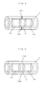
- Fig. 8 is a drawing showing astructure of a housing body and a plurality of magnets fixed thereto.
- Fig. 9 is a drawing showing another structure of a housing body and a plurality of magnets fixed thereto.
- Fig. 10 is a drawing describing a conventional optical isolator.
- Fig. 1 shows a sectional drawing showing a structure in case of a conventional optical Isolator having two Faraday rotators, wherein each first and second birefringent crystal plates, 1A, 3A, 1B, and 3B, respectively, are installed on both sides of Faraday rotators, 2A and 2B.
- Those optical elements are independently assembled and adjusted and are integrally fixed with the light-transmitting adhesive.
- Ultraviolet curing resin or thermosetting resin is used. The adoption of this structure enables down-sizing of an optical isolator unit and simplification of assembly work, which therefore allows accurate and easy assembly.
- the thickness of second birefringent crystal plates, 3A and 3B is designed to be (1+ 2 ) times the thickness of the first birefringent crystal plates, 1A and 1B.
- the Faraday rotators, 2A and 2B are magnetized by magnets, 4A and 4B, respectively,in opposite directions, at which the polarized wave aspects of transmitting light rotate by +45' and -45 ' respectively.
- Respective cylindrical magnets, 4A and 4B are formed by a magnetic body such as ferrite or the like . The place of them are selected so that respective Faraday rotators, 2A and 2B, can be positioned at approximately midway between them.
- integrally the plurality of magnets simplifies the fixing work with adhesive 6 by inserting the optical isolator unit composed of integrally formed optical elements into an integrally formed cylinder-type magnets, followed by adjustment to a predetermined position.
- the circumference of the cylinder-type magnet is covered with a metallic cylinder-type housing body, followed by fixing with an adhesive.
- the cylinder-type housing body holds the magnets and the spacers inside at a predetermined position and protects them.
- Fig. 2 is a sectional drawing showing another structure of a conventional optical isolator.
- the above-mentioned Faraday rotators,2A and 2B, and birefringent crystal plates, 1A, 3A, 1B, and 3B, are inserted into slots which are processed on the surface of silicon substrate 7 in the form of comb. Since the adhesive is not used in a path through which light passes these optical elements, the light path is not shut by the burning or alteration of the adhesive caused by transmitting light even if high energy light is transmitted, and reliability is high. Other points of this embodiment are the same as shown in Fig. 1. A rectangular plate is used for the optical element, while a square tube or plate is used for the magnets other than a cylinder.
- Fig. 3 shows an example of main body's structure of an optical isolator or the present invention formed integrally using rectangle plates.
- Fig. 4 shows a case of an integrally formed magnets in which magnetic spacer 8 is arranged between cylindrical magnets, 4A and 4B, where they are integrally fixed by screws 9.
- the spacer is preferably made of magnetic body.
- the spacer 8 is arranged between magnets and adjusted so that the Faraday rotators are positioned at the center of each magnet. As physical means fixing other than with screws, welding or adhesive can be applied.
- Fig. 5 shows a sectional drawing of a structure of another optical isolator in relation to the present invention, which forms a housing body by providing a ring-shape collar 12 on both ends of a cylindrical body 11 made of metal such as soft-iron, etc.
- the collar 12 is fixed. Both ends of the inserted magnets, 4A and 4B, are securely fixed at the collar 12, which is effective when both magnets are arranged so that repulsion is generated. Indeed, there may be a case of introducing a spacer 8 to a position of clearance 10.
- Fig. 6 and Fig. 7 show sectional drawings of a main body's structure of another optical isolator.
- optical elements and magnets are fixed by passing a screw 14 through a screw hole 13 provided in a cylinder-type spacer 8.
- Each optical element is integrally fixed with these contact surfaces by use of an ultraviolet curing resin 15, while a spacer 8 as well as magnets, 4A and 4B, are also fixed by use of a thermosetting adhesive.
- Fig. 7 shows a structure as shown in Fig. 6, in which a hole 16 is provided in a cylinder-type spacer 8, and optical elements and magnets are fixed by applying an adhesive 17 in this hole. Others are the same as those in Fig. 6.
- Fig. 8 and Fig. 9 show a structure of integrally formed magnets,4A and 4B, and a spacer 8 which are integrally fixed in a cylindrical-type housing body 5.
- Fig. 8 shows that the housing body 5 and the spacer 8 (even the magnets 4A and 4B may suffice this need) are subjected to direct through-welding, 18A and 18B, by use of a YAG laser, etc.
- Fig. 9 shows that, by providing a hole 19 on a housing body 5, the housing body and the magnets are fixed by physical means such as welding, adhesive or screws through this hole.
Landscapes
- Physics & Mathematics (AREA)
- Nonlinear Science (AREA)
- Engineering & Computer Science (AREA)
- Power Engineering (AREA)
- General Physics & Mathematics (AREA)
- Optics & Photonics (AREA)
Claims (9)
- Optische Einwegleitung/optischer Isolator, enthaltend:eine optische Einwegleitungseinheit mit mehreren optischen Elementen, derart dass die mehreren optischen Elemente mindestens zwei Faraday-Rotatoren (2A, 2B) enthalten, sowie mehrere doppelt brechende Kristallplatten (1A, 1B, 3A, 3B), die an beiden Seiten jedes Rotators angeordnet sind;einen Magnetaufbau mit mehreren Magneten, die an einem Abstandsstück fixiert sind, das zwischen den Magneten angeordnet ist, derart, dass der Magnetaufbau um den Rand der Faraday-Rotatoren zum Magnetisieren der Faraday-Rotatoren angeordnet ist; undeinen Gehäusekörper (5), der um den Umfang der mehreren Magneten angeordnet ist, derart, dassdie optische Einwegleitungseinheit ferner eine Vorrichtung zum Fixieren der Magnetanordnung - einerseits an dem Gehäusekörper und andererseits an der optischen Einwegleitungseinheit - bei der Stelle des Abstandsstücks enthält.
- Optische Einwegleitung nach Anspruch 1, dadurch gekennzeichnet, dass die mehreren optischen Elemente aneinander durch Verwendung eines Licht übertragenden Klebstoffs (6) haften.
- Opische Einwegleitung nach Anspruch 1, dadurch gekennzeichnet, dass sie ferner ein Substrat (7) enthält, mit einem in der Oberfläche hiervon vorgesehenen Schlitz, in das eines der optischen Elemente fest eingefügt ist.
- Optische Einwegleitung nach Anspruch 1, dadurch gekennzeichnet, dass die mehreren Magneten (4A, 4B) an dem Abstandstück (8) durch eine Vorrichtung fixiert ist, die ausgewählt ist aus der Gruppe bestehend aus Schweißen, Schrauben (9) oder Klebstoff.
- Optische Einwegleitung nach Anspruch 1, dadurch gekennzeichnet, dass das Abstandsstück aus einem Magnetmaterial hergestellt ist.
- Optische Einwegleitung nach Anspruch 1, dadurch gekennzeichnet, dass die optische Einwegleitungseinheit und die mehreren Magneten (4A, 4B) aneinander durch eine Vorrichtung fixiert ist, die aus der Gruppe bestehend aus Schweißen, Schrauben (14) oder Klebstoff (17) ausgewählt ist.
- Optische Einwegleitung nach Anspruch 1, dadurch gekennzeichnet, dass der Gehäusekörper (5) aus einem Zylinder (11) oder einem Zylinder (11) mit Ringen/Ansätzen (12) an beiden Enden hiervon besteht.
- Optische Einwegleitung nach Anspruch 1, dadurch gekennzeichnet, dass der Gehäusekörper (5) mit einer Durchgangsöffnung (19A, 19B) versehen ist und dass die mehreren Magneten (4A, 4B) an dem Gehäusekörper durch eine Vorrichtung, ausgewählt aus der Gruppe bestehend aus Schweißen (18A, 18B) Schrauben oder Klebstoff fixiert sind.
- Optische Einwegleitung nach Anspruch 1, dadurch gekennzeichnet, dass der Gehäusekörper (5) aus einem Metall hergestellt ist und dass die Fixiervorrichtung zum Fixieren des Gehäusekörpers an dem Abstandsstück (8) durch eine Durchgangs-Schweißvorrichtung gebildet ist.
Applications Claiming Priority (6)
| Application Number | Priority Date | Filing Date | Title |
|---|---|---|---|
| JP24449394 | 1994-10-11 | ||
| JP24449394 | 1994-10-11 | ||
| JP244493/94 | 1994-10-11 | ||
| JP7139195 | 1995-03-29 | ||
| JP7139195 | 1995-03-29 | ||
| JP71391/95 | 1995-03-29 |
Publications (2)
| Publication Number | Publication Date |
|---|---|
| EP0707230A1 EP0707230A1 (de) | 1996-04-17 |
| EP0707230B1 true EP0707230B1 (de) | 2001-03-07 |
Family
ID=26412495
Family Applications (1)
| Application Number | Title | Priority Date | Filing Date |
|---|---|---|---|
| EP95115972A Expired - Lifetime EP0707230B1 (de) | 1994-10-11 | 1995-10-10 | Optischer Isolator |
Country Status (3)
| Country | Link |
|---|---|
| US (1) | US6028702A (de) |
| EP (1) | EP0707230B1 (de) |
| DE (1) | DE69520251D1 (de) |
Families Citing this family (9)
| Publication number | Priority date | Publication date | Assignee | Title |
|---|---|---|---|---|
| DE19725720A1 (de) * | 1997-06-18 | 1998-12-24 | Alsthom Cge Alcatel | Optischer Isolator und Wellenlängenmuliplexer-Modul mit integriertem optischen Isolator |
| US6091866A (en) * | 1998-09-01 | 2000-07-18 | Cheng; Yihao | Optical isolator |
| US6288826B1 (en) * | 2000-01-05 | 2001-09-11 | Jds Uniphase Inc. | Multi-stage optical isolator |
| US6421177B1 (en) | 2000-03-03 | 2002-07-16 | Arroyo Optics, Inc. | Interleaving optical filter |
| AU2001288320A1 (en) | 2000-09-05 | 2002-03-22 | Arroyo Optics, Inc. | System and method for fabricating components of precise optical path length |
| US7961391B2 (en) * | 2008-03-13 | 2011-06-14 | Finisar Corporation | Free space isolator optical element fixture |
| JP6340176B2 (ja) * | 2013-08-09 | 2018-06-06 | 湖北工業株式会社 | 光デバイス |
| JP6863683B2 (ja) * | 2016-04-26 | 2021-04-21 | 信越化学工業株式会社 | 光アイソレータ |
| JP6860436B2 (ja) * | 2017-06-29 | 2021-04-14 | 信越化学工業株式会社 | 光アイソレータモジュール |
Family Cites Families (25)
| Publication number | Priority date | Publication date | Assignee | Title |
|---|---|---|---|---|
| JPS6479721A (en) * | 1987-09-21 | 1989-03-24 | Namiki Precision Jewel Co Ltd | Optical isolator |
| US4974944A (en) * | 1988-07-21 | 1990-12-04 | Hewlett-Packard Company | Optical nonreciprocal device |
| JPH0272419A (ja) * | 1988-09-08 | 1990-03-12 | Fanuc Ltd | 主軸制御装置 |
| JPH02108016A (ja) * | 1988-10-18 | 1990-04-19 | Hitachi Metals Ltd | 光アイソレータ |
| JPH02126219A (ja) * | 1988-11-04 | 1990-05-15 | Fuji Elelctrochem Co Ltd | 光アイソレータ |
| JPH03137616A (ja) * | 1989-10-23 | 1991-06-12 | Nec Corp | 光アイソレータおよび光アイソレータ内蔵半導体レーザモジュール |
| JPH03245118A (ja) * | 1990-02-22 | 1991-10-31 | Tokin Corp | 光アイソレータ並びにその製造方法 |
| JP2758693B2 (ja) * | 1990-04-18 | 1998-05-28 | 信越化学工業株式会社 | 光アイソレータおよびその製造方法 |
| US5341235A (en) * | 1990-04-18 | 1994-08-23 | Shin-Etsu Chemical Co., Ltd. | Optical isolator and method for preparing same |
| JPH0432816A (ja) * | 1990-05-30 | 1992-02-04 | Hitachi Metals Ltd | 光アイソレータ |
| US5151955A (en) * | 1990-06-20 | 1992-09-29 | Kabushiki Kaisha Shinkosha | Optical isolator |
| JP2618744B2 (ja) * | 1990-08-03 | 1997-06-11 | 富士電気化学 株式会社 | 光アイソレータの製造方法 |
| JPH04264515A (ja) * | 1991-02-20 | 1992-09-21 | Sumitomo Electric Ind Ltd | 光アイソレータ |
| JPH04264514A (ja) * | 1991-02-20 | 1992-09-21 | Sumitomo Electric Ind Ltd | 光アイソレータ |
| JPH04326320A (ja) * | 1991-04-26 | 1992-11-16 | Hoya Corp | 光アイソレータ |
| JPH0746177B2 (ja) * | 1991-05-28 | 1995-05-17 | 三菱瓦斯化学株式会社 | 光アイソレータ |
| JP3160319B2 (ja) * | 1991-07-25 | 2001-04-25 | 株式会社信光社 | 光アイソレータ |
| EP0533398A1 (de) * | 1991-09-19 | 1993-03-24 | AT&T Corp. | Optischer Isolator mit Polarisationsdispersionskorrektur |
| JPH05173090A (ja) * | 1991-12-25 | 1993-07-13 | Shimadzu Corp | 光カプラ |
| JP2757093B2 (ja) * | 1992-04-20 | 1998-05-25 | 富士電気化学株式会社 | 無偏波分散型光アイソレータ |
| JPH06194604A (ja) * | 1992-11-04 | 1994-07-15 | Tokin Corp | ファイバ付き光アイソレータ |
| JP2823468B2 (ja) * | 1993-02-16 | 1998-11-11 | 三菱電機株式会社 | 電波探知装置 |
| JP3112212B2 (ja) * | 1993-02-17 | 2000-11-27 | 住友電気工業株式会社 | 光アイソレータ |
| JPH06265819A (ja) * | 1993-03-10 | 1994-09-22 | Tokin Corp | 光アイソレータ |
| JP2786078B2 (ja) * | 1993-05-14 | 1998-08-13 | 信越化学工業株式会社 | ファラデー回転子および光アイソレータ |
-
1995
- 1995-10-10 EP EP95115972A patent/EP0707230B1/de not_active Expired - Lifetime
- 1995-10-10 DE DE69520251T patent/DE69520251D1/de not_active Expired - Lifetime
- 1995-10-10 US US08/544,406 patent/US6028702A/en not_active Expired - Fee Related
Also Published As
| Publication number | Publication date |
|---|---|
| EP0707230A1 (de) | 1996-04-17 |
| US6028702A (en) | 2000-02-22 |
| DE69520251D1 (de) | 2001-04-12 |
Similar Documents
| Publication | Publication Date | Title |
|---|---|---|
| EP0525208B1 (de) | Optischer isolator | |
| EP0512572B1 (de) | Optischer Isolator und Verfahren zu seiner Herstellung | |
| EP0707230B1 (de) | Optischer Isolator | |
| JP2000510965A (ja) | オプトアイソレータ | |
| US5841922A (en) | Optical fiber terminal with optical isolator and semiconductor laser module using the same | |
| EP0640862A1 (de) | Verfahren zum Zusammenfügen eines optischen Isolators und Verfahren zur Messung der Isolation | |
| JPH10133146A (ja) | キャピラリー型光アイソレータ | |
| JPH11167085A (ja) | 光アイソレータ及び光アイソレータ付き光ファイバ端子 | |
| JP4540155B2 (ja) | 光アイソレータ | |
| JP3739686B2 (ja) | 埋込型光アイソレータ | |
| JP2857502B2 (ja) | 光アイソレータ | |
| JP3075435B2 (ja) | 光アイソレータ | |
| US20040101226A1 (en) | Magnet isolator with integrated focusing apparatus | |
| US6529324B1 (en) | Optical component and method of manufacturing the same | |
| JP2916960B2 (ja) | 光アイソレータ用素子 | |
| JP3290474B2 (ja) | 半導体レーザアレイ用光アイソレータ | |
| JP2002196282A (ja) | 光アイソレータ | |
| US20030002128A1 (en) | Optical isolator | |
| JPH10142558A (ja) | 光アイソレータおよびその製造方法 | |
| JPH04233510A (ja) | 光アイソレータ | |
| WO2000049450A9 (en) | Optical circulator | |
| WO2000049450A2 (en) | Optical circulator | |
| JP2840707B2 (ja) | 光アイソレータ | |
| JP3881555B2 (ja) | 光ファイバ用フェルールとこれを用いた光アイソレータ付きスタブ及びレセプタクル | |
| JPH10319346A (ja) | 光アイソレータ |
Legal Events
| Date | Code | Title | Description |
|---|---|---|---|
| PUAI | Public reference made under article 153(3) epc to a published international application that has entered the european phase |
Free format text: ORIGINAL CODE: 0009012 |
|
| AK | Designated contracting states |
Kind code of ref document: A1 Designated state(s): DE FR GB IT |
|
| 17P | Request for examination filed |
Effective date: 19960419 |
|
| 17Q | First examination report despatched |
Effective date: 19981218 |
|
| GRAG | Despatch of communication of intention to grant |
Free format text: ORIGINAL CODE: EPIDOS AGRA |
|
| GRAG | Despatch of communication of intention to grant |
Free format text: ORIGINAL CODE: EPIDOS AGRA |
|
| GRAH | Despatch of communication of intention to grant a patent |
Free format text: ORIGINAL CODE: EPIDOS IGRA |
|
| GRAH | Despatch of communication of intention to grant a patent |
Free format text: ORIGINAL CODE: EPIDOS IGRA |
|
| GRAA | (expected) grant |
Free format text: ORIGINAL CODE: 0009210 |
|
| AK | Designated contracting states |
Kind code of ref document: B1 Designated state(s): DE FR GB IT |
|
| ITF | It: translation for a ep patent filed | ||
| REF | Corresponds to: |
Ref document number: 69520251 Country of ref document: DE Date of ref document: 20010412 |
|
| PG25 | Lapsed in a contracting state [announced via postgrant information from national office to epo] |
Ref country code: DE Free format text: LAPSE BECAUSE OF FAILURE TO SUBMIT A TRANSLATION OF THE DESCRIPTION OR TO PAY THE FEE WITHIN THE PRESCRIBED TIME-LIMIT Effective date: 20010608 |
|
| ET | Fr: translation filed | ||
| REG | Reference to a national code |
Ref country code: GB Ref legal event code: IF02 |
|
| PLBE | No opposition filed within time limit |
Free format text: ORIGINAL CODE: 0009261 |
|
| STAA | Information on the status of an ep patent application or granted ep patent |
Free format text: STATUS: NO OPPOSITION FILED WITHIN TIME LIMIT |
|
| 26N | No opposition filed | ||
| REG | Reference to a national code |
Ref country code: GB Ref legal event code: 746 Effective date: 20040728 |
|
| REG | Reference to a national code |
Ref country code: FR Ref legal event code: D6 |
|
| PGFP | Annual fee paid to national office [announced via postgrant information from national office to epo] |
Ref country code: GB Payment date: 20051005 Year of fee payment: 11 |
|
| PGFP | Annual fee paid to national office [announced via postgrant information from national office to epo] |
Ref country code: FR Payment date: 20051010 Year of fee payment: 11 |
|
| PGFP | Annual fee paid to national office [announced via postgrant information from national office to epo] |
Ref country code: IT Payment date: 20061031 Year of fee payment: 12 |
|
| GBPC | Gb: european patent ceased through non-payment of renewal fee |
Effective date: 20061010 |
|
| REG | Reference to a national code |
Ref country code: FR Ref legal event code: ST Effective date: 20070629 |
|
| PG25 | Lapsed in a contracting state [announced via postgrant information from national office to epo] |
Ref country code: GB Free format text: LAPSE BECAUSE OF NON-PAYMENT OF DUE FEES Effective date: 20061010 |
|
| PG25 | Lapsed in a contracting state [announced via postgrant information from national office to epo] |
Ref country code: FR Free format text: LAPSE BECAUSE OF NON-PAYMENT OF DUE FEES Effective date: 20061031 |
|
| PG25 | Lapsed in a contracting state [announced via postgrant information from national office to epo] |
Ref country code: IT Free format text: LAPSE BECAUSE OF NON-PAYMENT OF DUE FEES Effective date: 20071010 |