EP0701211B1 - Datenprozessor mit Adressübersetzungsmechanismus - Google Patents
Datenprozessor mit Adressübersetzungsmechanismus Download PDFInfo
- Publication number
- EP0701211B1 EP0701211B1 EP95113771A EP95113771A EP0701211B1 EP 0701211 B1 EP0701211 B1 EP 0701211B1 EP 95113771 A EP95113771 A EP 95113771A EP 95113771 A EP95113771 A EP 95113771A EP 0701211 B1 EP0701211 B1 EP 0701211B1
- Authority
- EP
- European Patent Office
- Prior art keywords
- address
- size
- data processor
- virtual page
- information
- Prior art date
- Legal status (The legal status is an assumption and is not a legal conclusion. Google has not performed a legal analysis and makes no representation as to the accuracy of the status listed.)
- Expired - Lifetime
Links
- 238000013519 translation Methods 0.000 title claims description 131
- 230000007246 mechanism Effects 0.000 title description 21
- 230000015654 memory Effects 0.000 claims description 151
- 238000000034 method Methods 0.000 claims description 109
- 230000008569 process Effects 0.000 claims description 71
- 238000012545 processing Methods 0.000 claims description 48
- 230000004044 response Effects 0.000 claims description 7
- 239000004065 semiconductor Substances 0.000 claims description 4
- 230000006386 memory function Effects 0.000 claims 3
- 238000010586 diagram Methods 0.000 description 13
- BDEDPKFUFGCVCJ-UHFFFAOYSA-N 3,6-dihydroxy-8,8-dimethyl-1-oxo-3,4,7,9-tetrahydrocyclopenta[h]isochromene-5-carbaldehyde Chemical compound O=C1OC(O)CC(C(C=O)=C2O)=C1C1=C2CC(C)(C)C1 BDEDPKFUFGCVCJ-UHFFFAOYSA-N 0.000 description 10
- 238000010276 construction Methods 0.000 description 8
- 238000001514 detection method Methods 0.000 description 5
- 230000009467 reduction Effects 0.000 description 5
- 230000000717 retained effect Effects 0.000 description 5
- 230000000694 effects Effects 0.000 description 4
- 101150068401 BSL1 gene Proteins 0.000 description 3
- 238000013507 mapping Methods 0.000 description 3
- 230000008859 change Effects 0.000 description 2
- 208000003443 Unconsciousness Diseases 0.000 description 1
- 230000001276 controlling effect Effects 0.000 description 1
- 230000010485 coping Effects 0.000 description 1
- 230000007547 defect Effects 0.000 description 1
- 238000011010 flushing procedure Methods 0.000 description 1
- 230000006870 function Effects 0.000 description 1
- 230000005764 inhibitory process Effects 0.000 description 1
- 238000004519 manufacturing process Methods 0.000 description 1
- 238000012986 modification Methods 0.000 description 1
- 230000004048 modification Effects 0.000 description 1
- 229910021421 monocrystalline silicon Inorganic materials 0.000 description 1
- 230000002093 peripheral effect Effects 0.000 description 1
- 230000001105 regulatory effect Effects 0.000 description 1
- 239000000758 substrate Substances 0.000 description 1
Images


Classifications
-
- G—PHYSICS
- G06—COMPUTING; CALCULATING OR COUNTING
- G06F—ELECTRIC DIGITAL DATA PROCESSING
- G06F12/00—Accessing, addressing or allocating within memory systems or architectures
- G06F12/02—Addressing or allocation; Relocation
- G06F12/08—Addressing or allocation; Relocation in hierarchically structured memory systems, e.g. virtual memory systems
- G06F12/10—Address translation
- G06F12/1027—Address translation using associative or pseudo-associative address translation means, e.g. translation look-aside buffer [TLB]
- G06F12/1036—Address translation using associative or pseudo-associative address translation means, e.g. translation look-aside buffer [TLB] for multiple virtual address spaces, e.g. segmentation
-
- G—PHYSICS
- G06—COMPUTING; CALCULATING OR COUNTING
- G06F—ELECTRIC DIGITAL DATA PROCESSING
- G06F15/00—Digital computers in general; Data processing equipment in general
- G06F15/16—Combinations of two or more digital computers each having at least an arithmetic unit, a program unit and a register, e.g. for a simultaneous processing of several programs
-
- G—PHYSICS
- G06—COMPUTING; CALCULATING OR COUNTING
- G06F—ELECTRIC DIGITAL DATA PROCESSING
- G06F12/00—Accessing, addressing or allocating within memory systems or architectures
- G06F12/02—Addressing or allocation; Relocation
- G06F12/08—Addressing or allocation; Relocation in hierarchically structured memory systems, e.g. virtual memory systems
- G06F12/10—Address translation
- G06F12/1027—Address translation using associative or pseudo-associative address translation means, e.g. translation look-aside buffer [TLB]
-
- G—PHYSICS
- G06—COMPUTING; CALCULATING OR COUNTING
- G06F—ELECTRIC DIGITAL DATA PROCESSING
- G06F2212/00—Indexing scheme relating to accessing, addressing or allocation within memory systems or architectures
- G06F2212/65—Details of virtual memory and virtual address translation
- G06F2212/652—Page size control
-
- Y—GENERAL TAGGING OF NEW TECHNOLOGICAL DEVELOPMENTS; GENERAL TAGGING OF CROSS-SECTIONAL TECHNOLOGIES SPANNING OVER SEVERAL SECTIONS OF THE IPC; TECHNICAL SUBJECTS COVERED BY FORMER USPC CROSS-REFERENCE ART COLLECTIONS [XRACs] AND DIGESTS
- Y02—TECHNOLOGIES OR APPLICATIONS FOR MITIGATION OR ADAPTATION AGAINST CLIMATE CHANGE
- Y02D—CLIMATE CHANGE MITIGATION TECHNOLOGIES IN INFORMATION AND COMMUNICATION TECHNOLOGIES [ICT], I.E. INFORMATION AND COMMUNICATION TECHNOLOGIES AIMING AT THE REDUCTION OF THEIR OWN ENERGY USE
- Y02D10/00—Energy efficient computing, e.g. low power processors, power management or thermal management
Definitions
- the present invention relates to a data processor having an address translation mechanism and, more particularly, to a data processor having a set associative type cache memory used as the address translation mechanism as disclosed in: Computer Architecture News, vol. 20, no. 2, 1 May 1992, pages 415 - 424, which supports two page sizes. More particularly, the present invention is intended to diversify the address translation method and relates to a technique which is effective if applied to a microcomputer.
- This address translation mechanism is a mechanism for translating the logical address generated by the central processing unit (CPU) into a physical address so as to realize a virtual memory.
- a translation lookaside buffer (as will also be shortly referred to as the "TLB") is packaged together with the central processing unit (CPU) in the data processor.
- the translation lookaside buffer is constructed, for example, as a buffer memory having an associative memory structure for latching a translation pair of the logical address and the physical address, which are recently used.
- the buffer memory having the associative memory structure can be exemplified by a full associative memory constructed of a CAM (i.e., Content Addressable Memory) having a comparing circuit construction in each memory cell, or a set associative memory capable of realizing a relatively high hit percentage by making use of a general purpose random access memory.
- a CAM i.e., Content Addressable Memory
- the associative memory type translation lookaside buffer is disclosed, for example, on pp. 287 and 288 of "Super-High Speed MOS Device" issued by Kabushiki Gaisha Baifukan on February 10, 1986.
- An object of the present invention is to provide a data processor which is equipped with an address translation mechanism capable of satisfying the specifications demanded by the user and having excellent using conveniences.
- a data processor supporting virtual memories divides a logical address space into units called the "logical pages” and translates the logical addresses into physical addresses (as called the "address translation"),on each of the logical pages.
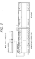
- the size of the logical page is made variable for each page, as exemplified in Fig. 1.
- a buffer memory 1 such as the translation lookaside buffer is used commonly for a plurality of logical pages each having a variable size.
- This buffer memory 1 to be used is exemplified by the set associative type cache memory having a plurality of banks 11 to 14 which individual have memory fields for storing corresponding informations including logical page numbers VPN and corresponding physical page numbers PPN corresponding the logical page numbers VPN and which are accessed by a commond index address 2.
- the maximum size of the logical pages to be supported is set to the power of two (i.e., the N-th power of two) of the minimum size, and the number of banks of the set associative type buffer memory is set to no less than the power of two (i.e., the N-th power of two).
- the logical addresses as designated by logical addresses of bits 0 to 31) of 4 GB (gigabytes)
- the logical pages have two kinds of sizes of 4 KB (kilobytes) and 1 KB.
- the buffer memory 1 includes four banks so that it is constructed into a 4-way set associative type cache memory.
- the offset of the logical address is set to the bits 0 to 11 of the logical address, and a logical page number vpn is set to the bits 12 to 31 of the logical address.
- the offset of the logical address is set to the bits 0 to 9 of the logical address, and the logical page number vpn is set to the bits 10 to 31 of the logical address.
- small letters vpn, ppn and asid designate the logical page number, physical page number and address space identifier (process number) to be used for the access and are differentiated from a logical page number VPN, a physical page number PPN and a address space identifier (process number) ASID, as designated by the large letters and used as either the entry of the buffer memory (or the translation lookaside buffer) or the page table entry.
- the sizes of the logical pages are shared for 4 KB and 1 KB, and a predetermined plural bits from the least one in the logical page address of the maximum page size are given as the index address.
- the buffer memory is indexed by using the five bits 12 to 16 in the logical address having the total of 32 bits. With this 5 bits of the index address, thirty two entries at the maximum can be assigned for one bank. In the case of four banks, as in the example of Fig. 1, four entries at the maximum can be assigned for one index address.
- the five bits (i.e., bits 12 to 16) from the least of the logical page number vpn are assigned to the aforementioned index address so that the maximum thirty two entries of an arbitrary virtual page number can be assigned to each bank (accordingly the total of one hundred and twenty eight entries).
- the two bits (i.e., the bits 10 and 11) from the least of the virtual page number vpn are not used for the indexing.
- the indexed entry is any of the four virtual page numbers, one of which is to be selected by the two bits (i.e., the bits 10 and 11) left unused for the index.
- the maximum size (i.e., 4 KB) of the virtual pages is set to the second power of two of the minimum size (i.e., 1 KB), and the bank number is set to the second power of two (i.e., four).
- the buffer memory i.e., the translation lookaside buffer
- the virtual page number of the entries to be assigned to one bank is subjected to a restriction of every 4 KB. This restriction exerts no influence upon the hit (i.e., TLB hit) rate if the virtual page numbers of the entries assigned to the translation lookaside buffer are consecutive. If these numbers are discrete, the hit rate is influenced to some extent. If, even in this case, the virtual page of 1 KB is subjected to the address mapping for every 2 KB, the influence can be reduced. This influence can be completely eliminated if the address mapping falls at every 4 KB.
- the bit number for the address comparison to be reflected upon the hit decision in comparator means 15 provided for each of the banks 11 to 14 has to be changed according to the logical (virtual) page size.
- the bits 10 and 11 of the logical address have to be compared in the case of the virtual page size of 1 KB, as contrary to the case of the virtual page size of 4 KB.
- the buffer memory 1 is set with the bit number of the fields for storing the corresponding information (or the translation pair) between the virtual page number and the physical page number so that all the bits to be compared may be covered.
- the buffer memory 1 is formed for each translation pair with a field indicating the virtual page size to be supported thereby, and the number of bits having addresses to be compared for the hit decision is changed according to the value (or size bit) SZ of the field.
- the items to have the comparison bit numbers changed are exemplified by both the virtual page number of the logical address and the virtual page number contained in the translation pair in the buffer memory.
- Reference characters hit1 to hit4 designate hit signals for informing the hit decision results in the individual banks 11 to 14 so that the TLB hit/miss are decided on the basis of the hit signals.
- the data processor for supporting the virtual memory comprises: a buffer memory including a set associative type cache memory having a plurality of banks which individually have memory fields for storing the corresponding informations between virtual page numbers and physical page numbers and which are to be individually accessed by a shared index address; and means for making variable a method of generating index addresses for the buffer memories.
- a buffer memory including a set associative type cache memory having a plurality of banks which individually have memory fields for storing the corresponding informations between virtual page numbers and physical page numbers and which are to be individually accessed by a shared index address; and means for making variable a method of generating index addresses for the buffer memories.
- the designation of the vpn (16 - 12) implies the information of the virtual page number containing, the bits 12 to 16 of the logical address.
- the designation of the VPN (31 - 17) implies the information of the virtual page number as the entries of the buffer memory corresponding to the bits 17 to 31 of the logical address.
- the data processor for supporting the virtual memory comprises the buffer memory 1 including a 4-way set associative type cache memory having the plural banks 11 to 14 which individually have memory fields for latching the corresponding informations between the virtual page number VPN and the physical page number PPN and which have their individual index addresses shared.
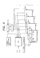
- the set to be replaced can be arbitrarily designated by executing a software by the central processing unit.
- the register MMUCR.RC is a register to be set with information of 2 bits for designating the aforementioned banks arbitrarily.
- one of the four banks 11 to 14, as designated by the selecting signals, that is, one entry designated by the index address 2 is a target of replacement.
- the bank designation by this hardware means can be arbitrarily changed by executing the software by the aforementioned central processing unit (CPU).
- the aforementioned hardware means is equipped with the register MMUCR.RC as counter means such as a random counter, as shown in Fig. 4.
- a control circuit CTRL contained in the aforementioned hardware means increments the counter means by one, in case the latched information is to be replaced for the buffer memory 1, and sets the incremented result to the bank number to be replaced, in case valid data are also latched in the indexed memory field of any bank (that is, in case each entry of each of the indexed banks has a valid bit V indicating the validity "1").
- the control circuit CTRL sets the counter means with the number of the bank including the entry latching no valid data. According to this predetermined rule, the bank to be replaced is designated. At this time, each bit of the aforementioned counter means is a target to be changed to an arbitrary value by the software which is executed by the central processing unit.
- the data processor for supporting the virtual memory comprises an address translation mechanism for dividing the logical address space into units called the "virtual pages" thereby to translate the logical address into the physical address at the page unit.
- This address translation mechanism comprises: a multiple virtual support for modifying or expanding the logical address for the address space identifier (asid), when each of the processes has an address translation information covering all over the logical space; and a single virtual support for neither modifying nor expanding the logical address for the address space identifier (asid) when a portion of the logical address space is exclusively assigned to the plural processes so that each process has the address translation information of the logical address space assigned thereto.
- the address translation mechanism can select the multiple virtual support and the single virtual support.
- each entry in the buffer memory is provided, as shown in Fig. 5, with not only the translation pair of the virtual page number VPN and the physical page number PPN but also the field of the address space identifier ASID.
- This content of this field is processed differently according to the single virtual support or the multiple virtual support.
- the content of the field of the address space identifier ASID is used in the multiple virtual support for deciding the retrieval hit/miss (i.e., TLB hit / TLB miss) for the buffer memory.
- the TLB hit is not decided if the information of the virtual page number VPN of the entry latched in the buffer memory matches the information of the virtual page address vpn and if the address space identifier ASID of the same entry mismatches the present address space identifier asid.
- the content of the field of the address space identifier ASID is used as the memory protecting information.
- the TLB miss occurs due to the difference in the address space identifier, it is decided by the software which of the difference in the address space identifier or in the virtual page address the miss is caused. In case the miss is caused by the difference in the address space identifier, the miss is treated as the protection error.
- the data processor for supporting the plural page sizes selectively is easily enabled to satisfy the demand for improving the using efficiency of the memory by each process by making the size of the virtual pages relatively small, in case the total memory capacity of the real memory to be packaged in the system is short. If, at this time, the maximum virtual page size is set to the power of two of the minimum size whereas the number of the banks of the set associative type buffer memory is set to the power of two of the same, the entries of the same number of any virtual page number can be latched on principle in the buffer memory independently of the size of the virtual page to be selected, even if the method of designating the index address is made identical to that for the maximum virtual page size.
- bit number of the address comparison to be reflected on the hit decision is changed by using the information for indicating size of the virtual page
- the bit number or position of the information to be compared for retrieving the buffer memory associatively can be changed according to the size of the virtual page. If the buffer memory for supporting the plural page sizes is realized by the set associative type cache memory, both the chip occupation area and the power consumption are reduced to halves as large as those of the construction of the CAM.
- these methods can be so selected according to the using mode, in which many processes are started in parallel in the multiple virtual support, as to suppress the reduction of the hit rate in the using mode.
- the reduction of the hit rate in the using mode, in which many processes are started in parallel in the multiple virtual support can be suppressed by modifying a portion of the logical address with the address space identifier (asid) using the same logical address thereby to index the buffer memory.
- the bank to be replaced can be arbitrarily decided by the software without fixing the replacement algorithm for replacing the translation pair of the buffer memory.
- the data processing conveniences it is possible in the data processing conveniences to satisfy the demand for latching a specific translation pair as the entry in the translation lookaside buffer at all times and the demand for preventing the specific address translation pair from being replaced.
- the provision of the register for instructing the target of replacement by the software can ensure the degree of freedom for the replacement according to the random, FIFO and LRU types in dependence upon the algorithm of the software.
- the means for the single virtual support and the multiple virtual support can improve the using conveniences of the address translation mechanism. These using conveniences can be improved better by selecting either of them through the software. If the address space identifier (ASID) in the multiple virtual support is used as the memory protecting information in the single virtual support, it is easily possible to complete the memory protection in case the single virtual support is selected.
- ASID address space identifier
- Fig. 7 shows an essential portion of a microcomputer according to one embodiment of the data processor of the present invention.
- the microcomputer of the present embodiment is formed over one semiconductor substrate of single crystal silicon by the well-known semiconductor integrated circuit manufacturing technique, although not especially limited thereto.
- Fig. 7 there are shown as representative circuit blocks a logical address bus VABUS, a physical address bus PABUS, data bus DBUS, a central processing unit (CPU) 3, a cache memory (CACHE) 4, a translation lookaside buffer (TLB) 1 as the buffer memory, and a TLB controller (TLBC) 5.
- the CPU 3 fetches an instruction from a not-shown program memory and processes the data in accordance with the description of the instruction.
- the CPU 3 outputs a logical address to the logical address bus VABUS and inputs/outputs the data through the data bus DBUS.
- the cache memory 4 is exemplified by the 4-way set associative type, although not especially limitative thereto.
- the band is indexed by using a portion of the logical address fed from the logical address bus VABUS.
- the physical address is latched in the tag portion of the entry.
- the tag portion thus indexed has its logical address translated by the translation lookaside buffer 1 and is compared with the physical address outputted to the physical address bus PABUS.
- the cache miss/hit are decided according to the comparison result.
- the microcomputer of the present embodiment divides the logical address space into the units called the "virtual page" and supports the virtual memory for the address translation from the logical address into the physical address at the page unit.
- the aforementioned translation lookaside buffer 1 latches the translation pair between a virtual page number VPN and a corresponding physical page number PPN, as the TLB entry.
- the TLB controller 5 translates the logical address outputted from the central processing unit 3 into the physical address by using the translation lookaside buffer 1.
- This translation lookaside buffer 1 is constructed of a 4-way set associative type cache memory having four banks sharing the index addresses. Although only one bank 11 is representatively shown in Fig.
- the address translation mechanism for the aforementioned virtual support is constructed of the aforementioned translation lookaside buffer 1, TLB controller 5 and CPU 3 and the system software or operating system for the address translation and the memory protection.
- the central processing unit 3 forms a logical address of 32 bits so as to support the logical address space of 4 GB.
- the logical address is made expandable by the later-described address space identifier (or space identifier) asid.
- Figs. 8(A) and 8(B) there is illustrated the address mapping of the logical address space which is supported.
- the fields, as “Mapped”, are those to be subjected to the address translation making use of the translation lookaside buffer (TLB) 1.
- H'FFFFFFFF (wherein H' designates a hexadecimal notation) to H'80000000 can be accessed in the privileged mode and decided as the address error if accessed in the user mode.
- a P4 field is a control space which is mapped with a peripheral control register.
- P1 and P2 fields are those, in which the corresponding physical addresses are fixed, and are not subjected to the address translation using the translation lookaside buffer 1. These fields P1 and P2 have their logical addresses translated into physical addresses by adding or subtracting a predetermined constant. In the privileged mode, therefore, no exception relating to the address translation, as started from the TLB miss, is made if the fields P1 and P2 are accessed.
- the P2 field is not cached by the cache memory CACHE, but the P1 field is not cached.
- the microcomputer of the present embodiment has the privileged mode and the user mode, as described above, and it is indicated by the value of the mode bit MD of a status register SR contained in the central processing unit 3 whether the microcomputer is operating in the privileged mode or the user mode.
- the privileged status (as set in the privileged mode)
- it is possible to access the address space (from P1 to P4) which will cause the address error if accessed in the user status (as set in the user mode) so that the privileged instruction or system control instruction, as cannot be executed in the user status, can be executed, as different from the user status.
- the P0 field and the P3 field are plurally divided at the unit called the virtual page, so that the logical address is translated into the physical address at the unit of the divided pages, although not especially limitative thereto.
- the virtual page size is 1 KB, as shown in Fig.
- the bits 0 to 9 are offset whereas the bits 10 to 31 are set to the virtual page numbers (or the virtual page addresses).
- the virtual page size is 4 KB
- the bits 0 to 11 are offset whereas the bits 12 to 31 are set to the virtual page numbers (or the virtual page addresses).
- the index for the translation lookaside buffer 1 is exemplified the information of the bit positions of the less significant five bits of the virtual page addresses of the page size of 4 KB, that is, the bits 12 to 16 of the logical addresses of 32 bits no matter whether the page size might be 4 KB or 1 KB.
- the physical addresses are acquired by acquiring the physical page number from the entry corresponding to the virtual page number of the logical address and by adding the offset information of the logical address to the less significant side of the physical page number.
- the information (i.e., the page table entry) to be fetched by the entry in the translation lookaside buffer 1 is generated in advance by the software and is latched in the external memory (e.g., the memory RAM of Fig. 22) which is omitted from Fig. 7.
- the page table entry for the virtual memory includes the description of the translation information indicating the correspondence between the virtual page number VPN and the physical page number PPN or the attributes of the access and is latched in the page table which is formed in the external memory.
- the entry latched in the page table is partially latched in the banks 11 to 14 of the aforementioned TLB 1.
- the addresses of the page table in the external memory are set in advance in the translation table register (TTB), as will be described with reference to Fig. 6. If a TLB miss occurs, the base address set in the translation tale register 53 and the virtual page number at the time of the miss are used by the CPU 3 to access the aforementioned page table thereby to determine the entry containing the physical page number corresponding to the virtual page number at that time. The entry thus determined is written to the bank in the TLB 1, for example. As a result, the physical address corresponding to the logical address at that time is generated.
- TLB translation table register
- the entry to be latched in each bank of the TLB 1 is conveniently divided into an address part and a data part, as shown in detail in Fig. 5.
- the address part is composed of the informations VPN (31 - 17) and VPN (11 - 10) of the virtual page number, a valid bit V (of 1 bit) indicating the validity of the entry, a space identifier ASID (of 8 bits), a size bit SZ (of 1 bit), and a share status SH (of 1 bit).
- the data part is composed of a protection PR (of 2 bits) for memory protection, the physical page number PPN (of 22 bits) corresponding to the virtual page number, a dirty bit D (of 1 bit), and a cacheable bit C (of 1 bit).
- the informations of the virtual page numbers latched by the address part are the bits 10 to 11 and the bits 17 to 31 of the logical addresses of 32 bits, from which the bits to be used for indexing the bit format are excluded.
- the former bits are expressed by the VPN (11 - 10) whereas the latter bits are expressed by the VPN (31 - 17).
- the space identifier ASID is used as belongs to a specific process to define the virtual page, and will also be called the "address space identifier".
- the protection PR is the data which are encoded to define the access right for the page, and the access right is defined in the modes shown in Fig. 9 by combining its values.
- the size bit SZ is a bit for designating the virtual page size, and the page size of 4 KB is designated by the logical value 1 whereas the page size of 1 KB is designated by the logical value 0.
- the multiple virtual support is defined to modify or expand the logical address by the address space identifier asid when each of the plural processes has the address translation information covering all over the logical space.
- a portion of the logical address space is exclusively assigned to the plural processes.
- the single virtual support is defined to neither modify nor expand the logical address by the address space identifier asid when each process has the address translation information of the logical address spaced assigned thereto.
- the logical address space is exclusively assigned among the plural processes so that each logical address space assigned to the process has its intrinsic address translation information, as shown in Fig. 20(B).
- This allows only one address translation table to exist.
- a certain logical address A is uniquely translated into a corresponding physical address D.
- the logical address space is assigned in a mutually overlapping manner among the plural processes.
- the address translation informations for the individual processes have to be contained in the mutually different address translation tables.
- the logical address A is transformed into different physical addresses B and C through mutually different address translation tables i and j.
- Fig. 19 illustrates the differences between the single virtual support and the multiple virtual support as to the logical space, the translation information and the protection.
- letters PR designate the protection information, as shown in Fig. 9.
- the aforementioned TLB controller 5 includes a controller (CTRL) 50, a page table entry high (PTEH) register 51, a page table entry low (PTEL) register 52, a translation table base (TTB) register 53, a TLB exception address (TEA) register 54, and a control (MMUCR) register 55.
- CTL controller
- PTEH page table entry high
- PTEL page table entry low
- TTB translation table base
- TLB exception address register 54 a control (MMUCR) register 55.
- These registers are coupled to the CPU 3, as will be described with reference to Fig. 22.
- at least the TEA register 54 and the MMUCR register 55 can be directly read/written by the CPU 3.
- the remaining registers 51 to 53 can also be accessed by the CPU 3.
- the PTEH register 51 and the PTEL register 52 are provided with the field which can latch the page table entry for updating or adding the entry of the TLB 1 at the time of a TLB miss.
- the PTEH register 51 is set with the space identifier asid of the present process from the central processing unit 3 by executing the software.
- the PTEH register 51 is also given a function to latch the virtual page address vpn of the TLB miss outputted by the CPU 3, if the TLB miss occurs.
- the offset of the logical address outputted from the CPU 3 is latched in the not-shown latch circuit in the CTRL 50.
- the base address of the present page table is latched in the TTB register 53.
- the TEA register 54 latches the logical address when an exception to the TLB or an address error exception occurs.
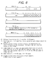
- index mode bit IX is at 1
- the index method using the asid (4 - 0) i.e., the bits 0 to 4 of the present space identifier asid and the bits 12 to 16 of the virtual page number vpn being outputted from the central processing unit 3, as shown in Fig. 3.
- IX 0, on the contrary, there is selected the index method using the bits 12 to 16 of the virtual page number vpn being outputted from the central processing unit 3, as shown in Fig. 2.
- a selector 18 of Fig. 7 selects either the output hashed by the exclusive OR gate XOR or the vpn (16 - 12) as the indexing address. The control for this selection is determined according to the value of the index mode bit IX by the select signal 550 outputted from the CTRL 50.
- the vpn (16 - 12) corresponding to the bits 12 to 16 are used to generate the index address 2 shared among the four banks 11 to 14 in the TLB. Since the virtual page number is expressed by 5 bits, as described above, the thirty two entries of each banks are selected and read out one by one by the shared index address 2.
- Each of the entries to be selected contains, as its information, the VPN (31 - 17), the VPN (11 - 10), the ASID, the SH, the SZ, the V, the PPN (31 - 10), the PR, the C and the D.
- the read VPN (31 - 17) are compared by a comparator 151 with the vpn (31 - 17) of the logical addresses outputted from the central processing unit 3; the VPN (11 - 10) are compared by a comparator 152 with the vpn (11 - 10) of the logical addresses outputted from the central processing unit 3; and the ASID read out is compared by a comparator 153 with the present space identifier asid latched by the PTEH register 51.
- a control logic 154 decides the miss/hit of the bank 11 by considering the values of the share status SH, the size bit SZ, the single virtual bit SV and the mode bit MD.
- the hit signal hit1 is the decision result of the miss/hit in the bank 11.
- the aforementioned comparators 151 to 153 and control logic 154 are provided for each of the banks 11 to 14.
- the hit signals hit2 to hit4 are representatively shown for the individual banks 12 to 14.
- the outputs of the individual comparators 151 to 153 are given the matched high level.
- the high levels of the hit signals hit1 to hit4 are used as the hit level.
- the control circuit 50 decides the TLB hit if any of the hit signals hit1 to hit4 is set to the hit level.
- Reference numeral 501 appearing in Fig. 7 designates a TLB hit signal for informing the CPU 3 of the decision result of the TLB hit/miss.
- the entry of the translation lookaside buffer 1 is replaced.
- the content of the entry to be replaced is latched in the PTEH register 51 and the PTEL register 52 so that the information to be replaced is fed from the PTEH register 51 and the PTEL register 52 is fed to and fetched in the TLB 1.
- the index method for selecting the entry to be replaced is identical to that at the aforementioned reading time, but which bank (or set) that entry is to be latched is decided by the value (MMUCR.RC) of the RC of the MMUCR register 55.
- Fig. 21 shows one example of the logical construction of the aforementioned control logic 154.
- Numeral 1541 designates a three-input AND gate; numeral 1542 a two-input OR gate; and numeral 1543 a two-input OR gate.
- the OR gate 1542 inputs both the output of the comparator 152 or the result of the comparison between the VPN (11 - 10) contained in the indexed TLB entry (i.e., the entry selected and read out by the index address) and the vpn (11 - 10) contained in the logical address and the size bit SZ coming from the aforementioned indexed TLB entry.
- the aforementioned OR gate 1543 inputs both the output of the comparator 153 or the result of comparison between the address space identifier ASID contained in the indexed TLB entry and the present address space identifier (or the address space identifier outputted from the PTEH register 51) asid and the shared bit SH coming from the aforementioned indexed TLB entry.
- the aforementioned address space identifier ASID owned by the TLB entry is used as the memory protecting information (or domain number).
- the share or non-share status is indicated by the shared bit SH.
- the non-share is indicated, the mismatch between the present address space identifier asid and the address space identifier ASID contained in the TLB entry is decided as the TLB miss in the multiple virtual support.
- the non-share is indicated, on the contrary, the mismatch between the address space identifiers asid and ASID is used in the single virtual support for detecting the TLB protection error exception.
- the control circuit 50 is equipped with an AND gate 502, as shown in Fig.
- the AND gate 502 In response to the inverted output of the aforementioned OR gate 1543, the signal virtual bit SV from the MMUCR register and the inverted signal of the mode bit MD in the status register in the central processing unit 3, the AND gate 502 generates a TLB protection error exception detection signal 503.
- This detection signal 503 has its high level at the detection level of the TLB protection error exception.
- the TLB miss is substantially decided. This status is set to the TLB protection error exception for the memory protection.
- Fig. 10 is a main flow chart showing the control of an address translation by the control circuit 50. This control is coarsely divided into a step L1 of indexing the translation lookaside buffer 1, a step L2 of comparing the addresses and checking the V-bit, a step L3 of checking the access right, and a step L4 of generating the physical address. These steps are controlled by the CPU 3 and the controller 5.
- the logical address to be used in this step is set to vpn (16 - 12) irrespective of its size.
- the MMUCR.IX is at 1, as shown in Fig. 11, the aforementioned used logical address is hashed to the indexing address by the asid (4 - 0).
- the vpn (16 - 12) is used as it is as the indexing address.
- the former index method is shown in Fig. 3 whereas the latter index method is shown in Fig. 2.
- the TLB 1 is indexed, one of the thirty two entries is selected and read out from each of the banks 11 to 14.
- Each entry to be selected contains the VPN (31 - 12), the VPN (11 - 10), the ASID, the SH, the SZ, the V, the PPN (31 - 10), the PR, the C and the D as its information.
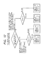
- Fig. 12 there is shown on example of the procedure of the address comparison to be executed at the step L2 of comparing the addresses and checking the V-bit.
- the procedure as shown herein, is based upon the logic of the control logic 154 shown in Fig. 21, but the detection of the TLB protection error exception is also considered as to the comparison of the space identifier ASID.
- How to determine the object of the address comparison to be reflected upon the hit signals hit1 to hit4 is decided, as follows. First of all, whether or not the space identifier is considered as the object of the address comparison is coarsely decided depending upon whether or not the SH is at 1. Whether or not the VPN (11 - 10) is considered as the object of the address comparison is decided depending upon whether or not the SZ is at 0.
- the infield data of the space identifier ASID are used as the memory protection information.
- the field of the space identifier ASID is excluded from the comparison object so that the virtual page assigned in the privileged mode to another process may also be accessed from the present process, that is, so that the TLB protection error exception may not be detected.
- the TLB entry is read from the TLB 1.
- SH share status
- the space identifier ASID is not considered in the detection of the TLB protection error exception. This is intended from the characteristics of the privileged mode to make it possible to access the virtual page assigned to another process from the present process.
- the size of 1 KB or 4 KB is selected as the size of the virtual page in accordance with the value of the size bit SZ in the TLB entry.
- the informations VPN (31 - 17) and VPN (11 - 10) in the TLB entry, as indexed in each bank are made the objects of comparison with the corresponding bits vpn (31 - 17) and vpn (11 - 10) of the logical address.
- the virtual page size is at 4 KB
- the VPN (11 - 10) in the TLB entry, as indexed in each bank, and the corresponding vpn (11 - 10) in the virtual page are excluded from the object of the comparison decision.
- the comparison objects (VPN (31 - 17, 11 - 10), vpn (31 - 17, 11 - 10), ASID and asid) are determined and compared. If a matching occurs in any bank as a result of the comparisons, a hit signal is outputted from the matching bank. The hits of the individual banks are outputted as the hit signals hit1 to hit4 so that the TLB hit is decided. If no hit signal is outputted from all the banks, that is, in the mismatching case, on the contrary, the TLB miss exception is detected. This result is informed by the signal 501 to the CPU 3, which processes the TLB miss exception, as will be described hereinafter.
- the V-bit in the entry is checked. In other words, the V-bit in the read entry is checked.
- the V-bit in the hit entry is 0 (invalid)
- the TLB invalid exception is detected and informed to the CPU 3.
- the decision result of the V-bit in the case of the TLB miss is used in the later-described entry replacement relating to the TLB miss.
- the space identifier ASID and the share status SH are considered at the time of checking the access right.
- the address space as expressed by the information in the TLB entry, is protected according to the aforementioned PR.
- the access right checking step L3 moreover, the access type is decided on whether the access is for the reading or writing operation, and the D-bit of the entry read from the TLB 1 is decided.
- the TLB initial page write exception is detected. Specifically, the TLB initial page write exception is detected under the conditions that the result of comparison between the logical address and the indexed TLB entry is the TLB hit, that the dirty bit D in the TLB entry is at 0 and that the access at this time is a write access.
- the content of this TLB initial page write exception processing will be described hereinafter.
- the physical address is generated, as shown in Fig. 14, in accordance with the size bit SZ of the indexed TLB entry.
- all the bits PPN (31 - 10) of the physical page number PPN is used the physical page address pa (31 - 10).
- the address (9 - 0) is added as the offset to the less significant side to generate the physical address pa.
- SZ 1 (the virtual page size is at 4 KB)
- the offset va (11 - 0) of the logical address va outputted from the CPU 3 is used as the offset pa (11 - 0) of the physical address pa.
- the PPN (31 - 12) having its less significant 2 bits ignored is used as the physical page address pa (31 -12).
- the address (11 - 0) is added as the offset to the less significant side to generate the physical address pa.
- Fig. 15 shows a hardware designation method of a bank to be replaced in the TLB miss exception, as detected at the step L2 of checking the address comparison and the V-bit.
- This control is uniquely executed by the control circuit 50 in accordance with its logical construction and uses the bit MMUCR.RC of the MMUCR register as counter means such as a random counter.
- the control circuit 50 decides the necessity for the replacement of the entry for the TLB 1.
- each bit of the aforementioned MMUCR.RC can have its value arbitrarily changed if the software is executed by the CPU 3.
- the bank number set in this register, as described above, can be further changed by the software.
- any bank can be made the object of replacement.
- Fig. 16 shows a processing procedure by the TLB miss handler for updating the TLB entry so as to cope with the aforementioned TLB miss exception.
- a load TLB instruction is used for updating the entry of the TLB 1.
- This load TLB instruction (as will also be expressed by the "LDTLB") is executed for the following processing by the CPU 3. Specifically, the values of the individual PTEH and PTEL registers 51 and 52 are written in the entries of the TLB 1. In this case, the entries to be written are those in the banks, which are indicated by the bank numbers set in the MMUCR.RC, although not especially limitative thereto, and are entries for indicating the logical addresses (i.e., bits 12 to 16) latched in the PTEH register 51, as the index addresses.
- the portion (i.e., the bits 10 to 31) of the logical addresses at that time, as outputted from the CPU 3, are latched in the aforementioned PTEH register 51.
- the entry at the replacement time is indicated by the index address of the same number as that of the index address at the time which the TLB miss exception occurs.
- the bank to be used for the replacement is decided by the bank number which is set in the MMUCR.RC.
- a page table is prepared in advance by the user in the external memory RAM, as shown in Fig. 22.
- a plurality of translation informations e.g., page table entries
- the addresses of this page table such as a start address is latched in advance as the base address in the register TTB 53.
- a plurality of page table entries individually corresponding to the logical addresses are arranged according to such rules as can retrieve the page table entries (containing the corresponding physical page number ppn, valid bit v, protection bit pr size bit sz, cacheable bit c, dirty bit d and status sh) corresponding to those logical addresses on the basis of the aforementioned base addresses and logical addresses as the start address, although not especially limitative thereto.
- the aforementioned TLB miss handler is described by the user.
- This TLB miss handler is started by the TLB miss handler when the TLB miss exception is detected.
- the information vpn (10 - 31) of the logical address upon the occurrence of the TLB miss is latched in the PTEH register 51.
- the space identifier asid at the occurrence of the TLB miss may also be latched in the PTEH register 51.
- the CPU 3 retrieves the aforementioned base table on the external memory by using the base address latched in the register TTB 53 and the logical address at the occurrence of the TLB miss.
- the page table entry corresponding to the logical address at the occurrence of the TLB miss has its content loaded, if discovered by that retrieval, in the PTEL register 52.
- the load TLB instruction is issued so that the entries of the TLB 1 are updated by the values of the individual registers PTEH and PTEL 51 and 52.
- the informations vpn and asid of the logical addresses at the occurrence of the TLB miss, as latched in the PTEH register 51 are adopted as the partial VPN and ASID of the TLB entries.
- the entries to be replaced at this time are those in the bank which is indicated by the bank number set in the MMUCR.RC, as described above, and are indicated by the same index address as that at the occurrence of the TLB miss.
- the aforementioned TLB invalid exception occurs in the case of the page fault in the TLB hit.
- the page table entry on the external memory is recovered to set the V-bit in the page table entry to the logical value 1.
- the PTEL register 52 is located with that page table entry from the external memory, and the aforementioned load TLB instruction is issued to up data the corresponding entry of the TLB 1 by the values of the individual PTEH and PTEL registers 51 and 52.
- the D-bit of the corresponding page table entry on the external memory is set to the logical value 1 to load the PTEL register 52 with that page table entry from the external memory.
- the aforementioned load TLB instruction is issued to update the corresponding entry of the TLB 1 by the values of the individual PTEH and PTEL registers 51 and 52.
- the informations vpn and asid of the logical addresses for causing the exception are latched in the PTEH register 51.
- the auxiliary memory and the main memory e.g., the external memory of Fig. 22
- it is necessary to decide whether or not the content of the page of the main memory to be replaced is to be copied back to the auxiliary memory.
- the dirty bit D is used for this decision.
- the virtual page number vpn of the logical address for causing the exception is written to the PTEH register 51, and the logical address is written to the TEA register 54. After this, the handler for solving that protection error is started.
- the increment is desired for registering a new bank entry at the time when the aforementioned TLB miss exception is to be coped with.
- TLB initial page write exception and TLB protection error exception on the contrary, it is desired not to increment the MMUCR.RC. This is because, in these counter-measures, only the D-bit or V-bit is necessary to change so that the TLB can be used more effectively by no registration in a new bank than by a registration in the original bank, although the present invention should not be limited thereto.
- Figs. 17 and 18 show the entirety of the exception detecting flow of the TLB 1 in case the multiple virtual support is indicated by setting the bit MMUCR.SV of the MMUCR register to 0.
- the TLB 1 is indexed (at S1) by a predetermined method according to the vpn of the logical address and the present space identifier asid.
- the information PR in the read entry is decided to be at 10 by the access in the user mode, it is further decided whether the access belongs to the read access type or the write access type. If the information is at 10, as shown in Fig. 9, the user access is allowed to have only the read access type. In case, therefore, the aforementioned access belongs to the write access type, the access type is different (i.e., the write of S 7), the TLB protection error exception (EX3) is detected.
- the TLB protection error exception (EX4) is detected if the read/write access type is contrary to the content of the PR (i.e., the write of S8).
- the access right to be allowed by the PR is different depending upon whether the CPU 3 is operating in the user mode or the in the privileged mode. In either event, in case the access is made in an access type other than that allowed by the PR, the TLB protection error exceptions (EX3 and EX4) are detected.
- the TLB initial write exception (EX5) is detected if the information D in the entry is at 0 (or unwritten page).
- Fig. 22 mainly shows the connection relations between the individual registers and the central processing unit CPU, as shown in Fig. 7.
- the logical addresses generated by the central processing unit CPU are fed through the internal logical address bus VABUS to the selector in the TLB control circuit TLBC.
- This selector decodes the logical addresses and generates a selection signal for selecting the registers in case these logical addresses are intrinsic ones assigned to the registers.
- the selector generates the selection signal C4 to select that register.
- the remaining registers PTEH, MMUCR, TEA and TTB are selected. In other words, these registers are address-mapped.
- the read/write of the selected register by the central processing unit are instructed through the not-shown internal control bus by the read/write control signals fed from the central processing unit to the individual registers. It is quite natural that the individual registers and the central processing unit CPU are connected to each other through the internal data bus DBUS, as shown. The individual registers are connected with both the control circuit 51 and the TLB 1, as shown in Fig. 7, but are not so shown in Fig. 22 so as to avoid the complicated illustration.
- the central processing unit is enabled to write the data in the registers by executing the software.
- the central processing unit is enabled to write the data in the registers by executing the software to output the logical addresses assigned to the registers to the bus VABUS, to output the data to the bus DBUS and instruct the write by the read/write signals. BY executing the software, the central processing unit can also read out the data from the registers. By thus executing the software, it is possible to write the logical space identifiers and the logical addresses at the TLB miss time in the PTEH register, to write the table entry at the replacing time in the PTEL register, to write the base address in the TTB register, and to write the logical addresses in the TEA register at the time of the protection error exception.
- the various control data shown in Fig. 6 can be written in the MMUCR register so that the specific bits can be used as the counter.
- the internal logical address bus VABUS is also connected with the control circuit CTRL and the TLB 1.
- the control circuit CTRL is equipped with a latch circuit for latching the offset of the logical address, as described above, so that the offset of the logical address from the internal logical address bus VABUS is latched.
- the logical address from the CPU 3 is fed to the TLB 1 through that internal logical address bus VABUS so that it is used as the index address and the retrieving address. It is quite natural that the aforementioned latch circuit disposed in the control circuit CTRL may latch not only the offset address but all the logical addresses.
- This drawing explicitly illustrates only the connection between the aforementioned PTEH register and TLB 1.
- the space identifier for deciding the miss/hit of the TLB 1 is set in this register and fed therefrom to the aforementioned TLB 1.
- the logical addresses are fed from that register to the TLB 1.
- the internal data bus DBUS and the internal physical address bus PABUS are connected with the external data bus DBUS and the external address bus ABUS through the external terminals TD and TA provided in this data processor. With these external buses, there are connected the external memories RAM and ROM, as shown.
- the external memory RAM is a volatile memory which is formed with the aforementioned various tables, although not especially limitative thereto.
- the external memory ROM is a non-volatile memory which latches the various programs (e.g., the software for the aforementioned handler).
- the page table entry and the TLB entry have the aforementioned size bit SZ so that the sizes of the virtual page can be set for each page.
- the 4-way set associative type translation lookaside buffer 1 is shared among the plural virtual pages capable of having their sizes set variable.
- two kinds of virtual page sizes of 1 KB and 4 KB are supported by the microcomputer.
- the method of designating the indexing addresses for the TLB 1 are made common between 4 KB and 1 KB.
- the bits 12 to 16, i.e., the vpn (16 - 12) are used for indexing the TLB 1.
- the index addresses are of 5 bits, the maximum thirty two entries can be retained for one bank (or way). Since the TLB 1 has the four banks 11 to 14, the maximum four entries can be retained for one index address.
- the index addresses are made to fall at the five bits vpn (16 - 12) from the least significant one of the virtual page number vpn.
- the entries of an arbitrary virtual page numbers can be retained at the thirty two entries for each bank (i.e., one hundred and twenty eight entries for all the banks).
- the vpn (11 - 10) of 2 bits from the least significant bit of the virtual page number vpn is not used for the indexing.
- the indexed entry indicates any of the four virtual page numbers (each having a page size of 1 KB), as selected by the index addresses of 5 bits.
- the 2 bits i.e., bits 10 and 11
- the maximum size of the virtual page is set to the N-th power of two of the minimum size, and the number of banks to be provided is also the N-th power of two.
- the virtual page has its minimum size set to 1 KB and its maximum size set to the second power of two of the former, i.e., 4 KB, and the number of banks to be provided is the second power of two, i.e., four.
- the translation lookaside buffer 1 can latch one hundred and twenty eight entries of an arbitrary virtual page number, as has the page size of 1 KB as a whole.
- the virtual page numbers of the entries to be retained in one bank is restricted to every 4 KB. This restriction exerts no influence upon the hit rate of the TLB 1 if the virtual page numbers of the entries retained by the translation lookaside buffer 1 are consecutive.
- This hit rate is influenced to some extent if the virtual page numbers are discrete. In this case, too, the influence can be reduced, if the virtual page of 1 KB is address-mapped for every 2 KB, and can be fully eliminated if address-mapped for every 4 KB.
- the four entries (E11), (E12), (E13) and (E14), as indicated by the index addresses of 5 bits, are set, from the four banks (11), (12), (13) and (14), respectively, with the translation information when the 2-bit vpn (11 - 10) is at "00", the translation information when the 2-bit vpn (11 - 10) is at "01”, the translation information when the 2-bit vpn (11 - 10) is at "10”, and the translation information when the 2-bit vpn (11 - 10) is at "11".
- the four entries (E11), (E12), (E13) and (E14), as indicated by the index addresses of 5 bits are set, from the four banks (11), (12), (13) and (14), respectively, with the translation information when the 2-bit vpn (11 - 10) is at "00", the translation information when the 2-bit vpn (11 - 10) is at "01”, the translation information when the 2-bit vpn (11 - 10) is at "10”, and the translation information when the 2-bit vpn
- the bit number of the address comparison for the hit decisions has to be changed according to the virtual page size, as described with reference to Fig. 12.
- the vpn (11 - 10) has to be compared with the VPN (11 - 10) unlike the case of 4 KB.
- the TLB 1 is provided with the memory fields of the VPN (31 - 17) and the VPN (11 - 10) and with the memory field of 22 bits even for the physical page number PPN.
- the TLB 1 is also provided in the data part of each entry with the size bit SZ indicating the virtual page size to be supported thereby, so that the bit number for the address comparison for the bit decision is changed according to the value of the size bit.
- the VPN (31 - 17) are compared with the corresponding bits of the logical address.
- the VPN (31 - 17) and the VPN (11 - 10) are compared with the corresponding bits of the logical address.
- the microcomputer for supporting the plural page sizes selectively can easily satisfy the demand for improving the memory using efficiency for each process by making the sizes of the virtual pages relatively small, in case the total memory capacity of the real memory to be packaged in the system is small.
- the translation lookaside buffer 1 is enabled, by setting the maximum virtual page size to the power of two of the minimum size and by the number of banks of the set associative type TLB 1 to no less than the power of two, to latch the entries of any virtual page number on principle, even if the method of indexing the index address is unified into that for the maximum virtual page size and no matter whether the selected virtual page size might be the maximum or the minimum.
- the number and position of the comparison target information for retrieving the translation lookaside buffer 1 associatively can be easily changed according to the size of the virtual page. If the translation lookaside buffer 1 for supporting the plural page sizes is realized by the set associative type cache memory, the chip occupation area and the power consumption can be reduced to halves of those of the case in which the same is constructed of the CAM.
- the method of decoding only one portion (i.e., the index addresses) of the logical addresses, as shown in Fig. 2, and the method of decoding the result of modifying one portion (i.e, the index addresses) of the logical addresses with one portion of the present address space identifier asid by the exclusive OR gate XOR, as shown in Fig. 3, can be instructed as the method of designating the index addresses of the TLB 1 in accordance with the logical values of the bit MMUCR.IX of the register MMUCR.
- the index methods can be so selected according to the using mode as to suppress the reduction of the hit rate. If, moreover, one portion of the logical addresses is modified by the address space identifier asid using the logical addresses to index the buffer memory, the reduction of the hit rate can be suppressed in the using mode in which many processes are started in parallel in the multiple virtual support.
- the TLB 1 is constructed as the 4-way set associative type cache memory which is provided with the plural banks 11 to 14 having their index addresses shared.
- the bank to be replaced can be arbitrarily designated by executing the software by the central processing unit 3.
- the bit MMUCR.RC is a field to be set with the information of 2 bits for designating the aforementioned bank arbitrarily. This set value is decoded by a decoder 17 of Fig. 4 to generate signals (BSL1 to BSL4) for selecting one of the four banks 11 to 14.
- the bit MMUCR.RC can also be used as the counter means such as a random counter.
- the power of two of the bit number of the MMUCR.RC is equalized to the number (4) of the banks of the aforementioned buffer memory 1.
- the control circuit (CTRL) 50 designates the banks in accordance with the following predetermined rules, as has been described with reference to Fig. 15. In case the replacement of the latched information for the TLB 1 is required (for a TLB miss), the MMUCR.RC is incremented by one.
- the incremented result is adopted as the bank number to be replaced.
- the bank number is set in the MMUCR.RC, and the bank having the set number is to be replaced.
- the individual bits of the MMUCR.RC are to have their values arbitrarily changed by the execution of the software by the central processing unit 3. Specifically, the MMUCR.RC is not restricted to the increment of +1 due to the occurrence of the TLB miss.
- the MMUCR.RC may be updated to exclude a specific value.
- various replacements can be achieved depending upon the algorithm of the software to be executed by the CPU 3. For example, the random replacement, the FIFO replacement starting from the initially loaded one, and the LRU (Least Recently Used) replacement starting from the last referred one can be easily realized by changing the method of updating the MMUCR.RC. As a result, it is possible to warrant the degree of freedom of the replacement.
- the microcomputer of the present embodiment it is possible to select the multiple virtual support, in which the logical address is modified or expanded by the address space identifier asid, in case the plural processes to be executed individually have the address translation information all over the logical space, and the single virtual support, in which the logical address is neither modified nor expanded by the address space identifier asid in case the individual processes have the address translation information of the logical address space assigned thereto.
- the control of those virtual supports is instructed by the value of the MMUCR.SV, as exemplified in Fig. 6.
- the value of this MMUCR.SV is arbitrarily set by the execution of the software by the central processing unit 3.
- the TLB 1 is provided with the fields for not only the virtual page number VPN, the physical page number PPN and the address space identifier ASID. These fields have different values in dependence upon whether the virtual support is single or multiple.
- the address space identifier ASID is used in the multiple virtual support for deciding the TLB hit/miss of the TLB 1, as described with reference to Fig. 17.
- the TLB hit is not determined unless the virtual page number VPN of the entry latched in the TLB 1 matches the virtual page address vpn and unless the address space identifier ASID of that entry matches the present address space identifier asid.
- the address space identifier ASID is used as the memory protecting information (or domain number).
- the access to the non-shared page by another process is processed as the TLB protection error exception by the software.
- the using conveniences of the address translation mechanism can be improved by setting the value of the MMUCR.SV through the CPU 3 to support the single virtual support and the multiple virtual support selectively.
- the memory protection can be easily made complete by using the address space identifier ASID of the multiple virtual support as the memory protection information in the single virtual support.
- the way number i.e., the bank number of the TLB can be increased to five or more such as eight.
- the page size is at 1 KB and 8 KB, for example, the way number (or bank number) of the TLB may be eight or more.
- the way number (or bank number) of the TLB may be four or more.
- the size of the address space to be supported by the microcomputer should not be limited to 4 GB, nor is limited the bit number of the logical address.
- the page size to be supported can be suitably changed to a suitable size, and the number of kinds to be supported can also be suitably changed.
- the virtual page number VPN to be latched as the TLB entry should not be restricted to the construction, from which is excluded the corresponding bits to be used for the index, as in the foregoing embodiment, but can latch all bits of the virtual page number as the TLB entry.
- MMU Memory Management Unit
- a data processor capable of supporting a plurality of page sizes without increasing the chip occupation area and the power consumption. It is also possible to realize an address translation mechanism capable of selecting the index methods.
- the address translation pair to be replaced can be given the degree of freedom. This degree of freedom can also be given to the virtual memory type to be supported. Thanks to these, it is possible to realize a data processor which is provided with an address translation mechanism capable of satisfying the specifications demanded by the user and having usable conveniences.
Landscapes
- Engineering & Computer Science (AREA)
- Theoretical Computer Science (AREA)
- Physics & Mathematics (AREA)
- General Engineering & Computer Science (AREA)
- General Physics & Mathematics (AREA)
- Computer Hardware Design (AREA)
- Software Systems (AREA)
- Memory System Of A Hierarchy Structure (AREA)
Claims (22)
- Datenprozessor mit einer virtuellen Speicherfunktion, bei der ein logischer Adressbereich in mehrere virtuelle Seiten aufgeteilt ist und eine virtuelle Adresse in eine absolute Adresse auf der Seiteneinheit übersetzt wird, umfassend:
einen Adressenübersetzungs-Pufferspeicher (1), der mehrere Banken (11 bis 14) enthält, wobei jede Bank (11 bis 14) mehrere Speicherfelder umfaßt, deren jedes virtuelle Seiteninformation enthält, die die absolute Seiteninformation einer virtuellen Seite repräsentiert, wobei der Datenprozessor ferner umfaßt:ein Auswahlelement, das ein Speicherfeld aus den Banken (11 bis 14) in Übereinstimmung mit einem ersten vorbestimmten Teil der virtuellen Adresse auswählt; undein Vergleichselement, das die virtuelle Seiteninformation in dem ausgewählten Speicherfeld mit einem zweiten Teil der virtuellen Adresse vergleicht, wobei der Datenprozessor dadurch gekennzeichnet ist, daßjedes der Speicherfelder zusätzlich Größeninformation der virtuellen Seite enthält und dadurch, daß der zweite Teil der virtuellen Adresse Bits der virtuellen Adresse enthält, die entsprechend der Größeninformation im ausgewählten Speicherfeld bestimmt werden. - Datenprozessor nach Anspruch 1, wobei eine Größe der virtuellen Seite zwischen einer maximalen Größe und einer minimalen Größe eingestellt wird, wobei die maximale Größe ein 2N-Vielfaches der minimalen Größe ist, und wobei die Anzahl der Banken des Pufferspeichers nicht kleiner als 2N ist.
- Datenprozessor nach Anspruch 2, wobei der erste Teil der virtuellen Adresse zum Auswählen des Speicherfelds aus jeder der Banken 11 bis 14 Adressenorte hat, die in der virtuellen Adresse fixiert sind, und wobei die fixierten Adressenorte durch Adressenorte in der virtuellen Adresse bestimmt werden, durch die das Speicherfeld aus einer der Banken ausgewählt wird, wenn die virtuelle Seite die maximale Größe aufweist.
- Datenprozessor nach Anspruch 3, wobei die virtuelle Seiteninformation, die im Speicherfeld gespeichert ist, ein Feld zum Speichern erster Bits zum Vergleich mit dem zweiten Teil der virtuellen Adresse enthält, wenn die virtuelle Seite die maximale Größe hat, und ein Feld zum Speichern zweiter Bits, die nicht mit dem zweiten Teil der logischen Adresse verglichen werden, wenn die virtuelle Seite die maximale Größe hat, und die mit dem zweiten Teil der logischen Adresse verglichen werden, wenn die virtuelle Seite die minimale Größe aufweist, und
wobei unabhängig davon, ob der Vergleich für die zweiten Bits durchgeführt wurde, eine Trefferentscheidung entsprechend der Größeninformation bestimmt wird. - Datenprozessor nach Anspruch 1, wobei der Adressenübersetzungs-Pufferspeicher (1) assoziativ ist, ferner umfassend:Einrichtung zum Bereitstellen eines Steuersignals; undein Indexadressen-Erzeugungselement, das mindestens einen Teil der virtuellen Adresse und des Steuersignals empfängt, wobei das Indexadressen-Erzeugungselement eine Indexadresse zum Auswählen eines Speicherfelds aus jeder der mehreren Banken erzeugt, und wobei das Indexadressen-Erzeugungselement dem Kontrollsignal entsprechend unterschiedliche Indexadressen erzeugt.
- Datenprozessor nach Anspruch 5, wobei das Indexadressen-Erzeugungselement ein erstes Element enthält, das basierend auf Informationen, die einem Prozeß entsprechen, der die virtuelle Adresse benutzt, den Teil der virtuellen Adresse verändert, und ein Element, das den Abschnitt der virtuellen Adresse oder eine Ausgabe des ersten Elements als die Indexadresse entsprechend dem Steuersignal bereitstellt.
- Datenprozessor nach Anspruch 1, einschließlich einer Zentraleinheit (3), wobei der Adressenübersetzungs-Pufferspeicher (1) Satz-assoziativ ist, ferner umfassend:
ein Bestimmungselement, auf das die Zentraleinheit zugreift und das eine Bank einschließlich einem Speicherfeld bestimmt, in dem Information zu ersetzen ist, wobei die Bank, in der Information zu ersetzen ist, durch eine Software bestimmt wird, die von der Zentraleinheit 3 ausgeführt wird. - Datenprozessor nach Anspruch 7, wobei das Bestimmungselement ein Register enthält, in dem die Information zum Bestimmen der Bank, in der Information zu ersetzen ist, durch das Ausführen einer Software durch die Zentraleinheit (3) bestimmt wird.
- Datenprozessor nach Anspruch 1, wobei der Adressenübersetzungs-Pufferspeicher (1) Satz-assoziativ ist, ferner umfassend:ein Element, das eine von mehreren Banken (11 bis 14) bestimmt, die ein Speicherfeld mit Information enthält, die entsprechend einer vorbestimmten Regel zu ersetzen ist; undeine Zentraleinheit (3), die mit dem Element gekoppelt ist und die die Bestimmung der Bank durch das Element der eine vorbestimmte Software ausführenden Zentraleinheit (3) ändert.
- Datenprozessor nach Anspruch 9, wobei das Bestimmungselement ein Zählelement enthält, und wobei die vorbestimmte Regel zur Bestimmung der Bank (1 bis 14), die die zu ersetzende Information enthält,das Inkrementieren der Zähleinheit entsprechend einer Anfrage zum Ersetzen der Information vom Satz-assoziativen Zwischenspeicher (1) umfaßt,das Einstellen des inkrementierten Ergebnisses, als die Bank (11 bis 14), die zu ersetzende Information enthält, wenn jede der Banken (11 bis 14) effektive Daten speichert, unddas Einstellen des Zählelements mit der Nummer einer Bank (11 bis 14), die keine effektiven Daten speichert, als die Bank (11 bis 14), die zu ersetzende Information enthält, wenn der Satz-assoziative Zwischenspeicher (1) eine Bank enthält, die keine effektiven Daten speichert; undwobei die Zentraleinheit das Zählelement beim Ausführen der vorbestimmten Software ändert, wobei die Bestimmung der Bank geändert wird.
- Datenprozessor nach Anspruch 1, umfassend
eine Prozeßeinheit, die die logische Adresse erzeugt, welche eine Indexadresse, eine Vergleichsadresse und eine Distanzadresse enthält; und wobei der Adressenübersetzungs-Pufferspeicher (1) ein Adressenübersetzungsspeicher (TLB) ist, der die virtuelle Adresse, die von der Prozeßeinheit erzeugt ist, in eine absolute Adresse übersetzt, wobei der Adressenübersetzungsspeicher (TLB) (1) umfaßt:mehrere Banken (11 bis 14) mit jeweils mehreren Einträgen, die jeweils eine virtuelle Seitennummer, die die virtuelle Seite angibt, Größeninformation, die die Größe der virtuellen Seite angibt, und eine absolute Seitennummer, die zur virtuellen Seitennummer paßt, haben,einen Selektor, der einen von der Indexadresse bestimmten Eintrag aus jeder der Banken entsprechend der Indexadresse auswählt; undeinen Komparator (151 bis 153), der die virtuellen Seitennummer des ausgewählten Eintrags mit der Vergleichsadresse vergleicht, wobei eine Bitnummer der zu vergleichenden virtuellen Seitennummer durch die Größeninformation im ausgewählten Eintrag festgelegt wird, undwobei die absolute Adresse aus der absoluten Seitennummer im ausgewählten Eintrag und der Distanzadresse erzeugt wird. - Datenprozessor nach Anspruch 11, wobei der Prozessor und der Adressenübersetzungsspeicher (TLB) auf einem Halbleiterchip ausgebildet sind.
- Datenprozessor nach Anspruch 12, wobei eine erste Größe der virtuellen Seite die N-te Potenz von Zwei einer zweiten Größe der virtuellen Seite beträgt, und wobei eine Anzahl der Banken 11 bis 14 nicht größer als N-te Potenz von Zwei ist.
- Datenprozessor nach Anspruch 11, wobei der Datenprozessor unter Verwendung der virtuellen Speicherfunktion mehrere Prozesse ausführt, wobei der Datenprozessor ferner umfaßt:ein vom Prozessor einstellbares Steuerbit, undein Register zur Ausgabe einer Prozeßnummer zum Anzeigen eines Prozesses unter mehreren Prozessen, undwobei der Selektor die Indexadresse mit einem Abschnitt der Prozeßnummer verändert und einen Eintrag auswählt, indem er die geänderte Indexadresse verwendet, wenn das Steuerbit in einem ersten Zustand eingestellt ist, und wobei der Selektor einen Eintrag unter Verwendung der Indexadresse auswählt, wenn das Steuerbit in einem zweiten Zustand eingestellt ist.
- Datenprozessor nach Anspruch 14, wobei der Selektor ein ausschließliches logisches Element umfaßt, das die Indexadresse und den Abschnitt der Prozeßnummer empfängt und einen Dekoder, der entweder eine Ausgabe des exklusiven logischen Elements oder der Indexadresse in Übereinstimmung mit dem ersten Steuerbit dekodiert.
- Datenprozessor nach Anspruch 14, wobei jeder von mehreren Einträgen eine Prozeßnummer umfaßt, die mit der Prozeßnummer aus dem Register zu vergleichen ist.
- Datenprozessor nach Anspruch 12, ferner umfassend:ein durch den Prozessor einstellbares Steuerbit und einen zweiten Selektor, der eine von mehreren Banken (11 bis 14) entsprechend dem Steuerbit bestimmt, wenn keine effektive Information in einem der von der Indexadresse ausgewählten Einträge gespeichert ist,wobei eine absolute Seitennummer in den Eintrag geschrieben wird, der von der Indexadresse bestimmt ist, und der in der Bank enthalten ist, die vom zweiten Selektor bestimmt ist, wobei die Information in dem Eintrag im Adressenübersetzungsspeicher (TLB) (1) ersetzt wird.
- Datenprozessor nach Anspruch 12, wobei der Datenprozessor unter Verwendung der virtuellen Speicherfunktion mehrere Prozesse ausführt, ferner umfassendein Register, das eine Prozeßnummer zum Spezifizieren eines von mehreren Prozessen speichert,wobei jeder der mehreren Einträge ein Prozeßfeld zum Speichern einer Prozeßnummer zum Spezifizieren eines Prozesses enthält sowie ein Teilfeld zum Speichern einer Teilinformation, die anzeigt, ob eine virtuelle Seite, die von einer virtuellen, in dem Eintrag gespeicherten Seitennummer angezeigt wird, von mehreren Prozessen geteilt wird, undwobei durch die Teilinformation entschieden wird, ob ein Vergleich zwischen der Prozeßnummer, die in dem Register gespeichert ist, und der Prozeßnummer, die in dem Prozeßfeld gespeichert ist, durch den Komparator ausgeführt wird.
- Datenprozessor nach Anspruch 11, ferner umfassend ein von der Prozeßeinheit einstellbares Bankbestimmungselement, und wobei der Adressenübersetzungsspeicher (TLB) (1) ferner umfaßt:einen Komparator (151 bis 153), der die virtuelle Seitennummer aus dem ausgewählten Eintrag mit der Vergleichsadresse vergleicht; undeinen Bankauswähler, der eine Bank bestimmt, die von dem Bankbestimmungselement dazu bestimmt ist, den Austausch eines Eintrags auszuführen, wenn der Komparator anzeigt, daß eine virtuelle Seitennummer, die zu der Vergleichsadresse gehört, nicht in dem ausgewählten Eintrag gespeichert ist.
- Datenprozessor nach Anspruch 19, wobei der Datenprozessor auf einem Halbleiterchip ausgebildet ist.
- Datenprozessor nach Anspruch 1, wobei eine Größe der virtuellen Seite auf eine maximale und eine minimale Größe einstellbar ist, und wobei die Beziehung zwischen der Anzahl der Banken, der maximalen und der minimalen Größe durch N ≥ Smax/Smin dargestellt ist, wobei N die Anzahl der Banken, Smax die maximale Größe und Smin die minimale Größe angibt, und wobei die maximale Größe eine Potenz von zwei der minimalen Größe ist.
- Datenprozessor nach Anspruch 12,
wobei die Größe der virtuellen Seite auf eine erste und zweite Größe einstellbar ist und wobei die Beziehung zwischen der Anzahl der Banken, der ersten Größe und der zweiten Größe durch N ≥ S1/S2 dargestellt ist, wobei N die Anzahl der Banken, S1 die erste Größe und S2 die zweite Größe darstellt, und wobei die erste Größe eine Potenz von zwei der zweiten Größe ist.
Priority Applications (1)
| Application Number | Priority Date | Filing Date | Title |
|---|---|---|---|
| EP99120560A EP0977123A3 (de) | 1994-09-09 | 1995-09-01 | Datenprozessor mit Adressübersetzungsmechanismus |
Applications Claiming Priority (9)
| Application Number | Priority Date | Filing Date | Title |
|---|---|---|---|
| JP24199394 | 1994-09-09 | ||
| JP241993/94 | 1994-09-09 | ||
| JP24199394 | 1994-09-09 | ||
| JP8606895 | 1995-03-17 | ||
| JP8606895 | 1995-03-17 | ||
| JP86068/95 | 1995-03-17 | ||
| JP24087195 | 1995-08-25 | ||
| JP24087195A JP3740195B2 (ja) | 1994-09-09 | 1995-08-25 | データ処理装置 |
| JP240871/95 | 1995-08-25 |
Related Child Applications (1)
| Application Number | Title | Priority Date | Filing Date |
|---|---|---|---|
| EP99120560.0 Division-Into | 1999-10-15 |
Publications (3)
| Publication Number | Publication Date |
|---|---|
| EP0701211A2 EP0701211A2 (de) | 1996-03-13 |
| EP0701211A3 EP0701211A3 (de) | 1997-10-15 |
| EP0701211B1 true EP0701211B1 (de) | 2001-04-18 |
Family
ID=27305071
Family Applications (2)
| Application Number | Title | Priority Date | Filing Date |
|---|---|---|---|
| EP99120560A Withdrawn EP0977123A3 (de) | 1994-09-09 | 1995-09-01 | Datenprozessor mit Adressübersetzungsmechanismus |
| EP95113771A Expired - Lifetime EP0701211B1 (de) | 1994-09-09 | 1995-09-01 | Datenprozessor mit Adressübersetzungsmechanismus |
Family Applications Before (1)
| Application Number | Title | Priority Date | Filing Date |
|---|---|---|---|
| EP99120560A Withdrawn EP0977123A3 (de) | 1994-09-09 | 1995-09-01 | Datenprozessor mit Adressübersetzungsmechanismus |
Country Status (5)
| Country | Link |
|---|---|
| US (2) | US5796978A (de) |
| EP (2) | EP0977123A3 (de) |
| JP (1) | JP3740195B2 (de) |
| KR (1) | KR100368196B1 (de) |
| DE (1) | DE69520718T2 (de) |
Families Citing this family (122)
| Publication number | Priority date | Publication date | Assignee | Title |
|---|---|---|---|---|
| US5918251A (en) * | 1996-12-23 | 1999-06-29 | Intel Corporation | Method and apparatus for preloading different default address translation attributes |
| US5950228A (en) * | 1997-02-03 | 1999-09-07 | Digital Equipment Corporation | Variable-grained memory sharing for clusters of symmetric multi-processors using private and shared state tables |
| KR100263672B1 (ko) * | 1997-05-08 | 2000-09-01 | 김영환 | 가변적인 페이지 크기를 지원하는 어드레스 변환장치 |
| JPH10333971A (ja) * | 1997-05-28 | 1998-12-18 | Sony Corp | データ演算装置 |
| DE19735948C1 (de) * | 1997-08-19 | 1998-10-01 | Siemens Nixdorf Inf Syst | Verfahren zur Verbesserung der Steuerungsmöglichkeit in Datenverarbeitungsanlagen mit Adreßübersetzung |
| JP3457644B2 (ja) * | 1997-11-06 | 2003-10-20 | 株式会社日立製作所 | データ処理装置およびデータ処理システム |
| DE69815482T2 (de) * | 1997-12-24 | 2004-04-29 | Texas Instruments Inc., Dallas | Computer Anordnung mit Prozessor und Speicher-Hierarchie und sein Betriebsverfahren |
| US6289431B1 (en) * | 1998-01-26 | 2001-09-11 | Intel Corporation | Method and apparatus for accessing more than 4 Gigabytes of physical memory with 4-byte table entries |
| US6266754B1 (en) * | 1998-05-29 | 2001-07-24 | Texas Instruments Incorporated | Secure computing device including operating system stored in non-relocatable page of memory |
| US6657959B1 (en) | 1998-06-27 | 2003-12-02 | Intel Corporation | Systems and methods for implementing ABR with guaranteed MCR |
| US6735773B1 (en) | 1998-06-27 | 2004-05-11 | Intel Corporation | Method and apparatus for issuing commands to a network processor configured to provide a plurality of APIs |
| US6603768B1 (en) | 1998-06-27 | 2003-08-05 | Intel Corporation | Multi-protocol conversion assistance method and system for a network accelerator |
| US6311212B1 (en) * | 1998-06-27 | 2001-10-30 | Intel Corporation | Systems and methods for on-chip storage of virtual connection descriptors |
| US6728249B2 (en) | 1998-06-27 | 2004-04-27 | Intel Corporation | System and method for performing cut-through forwarding in an ATM network supporting LAN emulation |
| US6724767B1 (en) | 1998-06-27 | 2004-04-20 | Intel Corporation | Two-dimensional queuing/de-queuing methods and systems for implementing the same |
| US6604136B1 (en) | 1998-06-27 | 2003-08-05 | Intel Corporation | Application programming interfaces and methods enabling a host to interface with a network processor |
| US6226731B1 (en) * | 1998-09-08 | 2001-05-01 | International Business Machines Corporation | Method and system for accessing a cache memory within a data-processing system utilizing a pre-calculated comparison array |
| DE19842849C2 (de) * | 1998-09-18 | 2001-02-01 | Siemens Ag | Verfahren und Anordnung zum Übertragen von digitalen Daten |
| US6910109B2 (en) * | 1998-09-30 | 2005-06-21 | Intel Corporation | Tracking memory page state |
| US6542983B1 (en) | 1999-10-01 | 2003-04-01 | Hitachi, Ltd. | Microcomputer/floating point processor interface and method |
| US6598128B1 (en) | 1999-10-01 | 2003-07-22 | Hitachi, Ltd. | Microprocessor having improved memory management unit and cache memory |
| US6408381B1 (en) | 1999-10-01 | 2002-06-18 | Hitachi, Ltd. | Mechanism for fast access to control space in a pipeline processor |
| US7266728B1 (en) | 1999-10-01 | 2007-09-04 | Stmicroelectronics Ltd. | Circuit for monitoring information on an interconnect |
| US6629207B1 (en) | 1999-10-01 | 2003-09-30 | Hitachi, Ltd. | Method for loading instructions or data into a locked way of a cache memory |
| US6591369B1 (en) | 1999-10-01 | 2003-07-08 | Stmicroelectronics, Ltd. | System and method for communicating with an integrated circuit |
| US6590907B1 (en) | 1999-10-01 | 2003-07-08 | Stmicroelectronics Ltd. | Integrated circuit with additional ports |
| US7072817B1 (en) | 1999-10-01 | 2006-07-04 | Stmicroelectronics Ltd. | Method of designing an initiator in an integrated circuit |
| US7000078B1 (en) * | 1999-10-01 | 2006-02-14 | Stmicroelectronics Ltd. | System and method for maintaining cache coherency in a shared memory system |
| US6487683B1 (en) | 1999-10-01 | 2002-11-26 | Stmicroelectronics Limited | Microcomputer debug architecture and method |
| JP2001142692A (ja) * | 1999-10-01 | 2001-05-25 | Hitachi Ltd | 2つの異なる固定長命令セットを実行するマイクロプロセッサ、マイクロコンピュータおよび命令実行方法 |
| US6463553B1 (en) | 1999-10-01 | 2002-10-08 | Stmicroelectronics, Ltd. | Microcomputer debug architecture and method |
| US6693914B1 (en) | 1999-10-01 | 2004-02-17 | Stmicroelectronics, Inc. | Arbitration mechanism for packet transmission |
| US6567932B2 (en) | 1999-10-01 | 2003-05-20 | Stmicroelectronics Limited | System and method for communicating with an integrated circuit |
| US6615370B1 (en) | 1999-10-01 | 2003-09-02 | Hitachi, Ltd. | Circuit for storing trace information |
| US6574651B1 (en) | 1999-10-01 | 2003-06-03 | Hitachi, Ltd. | Method and apparatus for arithmetic operation on vectored data |
| US6349371B1 (en) | 1999-10-01 | 2002-02-19 | Stmicroelectronics Ltd. | Circuit for storing information |
| US6601189B1 (en) | 1999-10-01 | 2003-07-29 | Stmicroelectronics Limited | System and method for communicating with an integrated circuit |
| US6820195B1 (en) | 1999-10-01 | 2004-11-16 | Hitachi, Ltd. | Aligning load/store data with big/little endian determined rotation distance control |
| US6530047B1 (en) | 1999-10-01 | 2003-03-04 | Stmicroelectronics Limited | System and method for communicating with an integrated circuit |
| US6449712B1 (en) | 1999-10-01 | 2002-09-10 | Hitachi, Ltd. | Emulating execution of smaller fixed-length branch/delay slot instructions with a sequence of larger fixed-length instructions |
| US6665816B1 (en) | 1999-10-01 | 2003-12-16 | Stmicroelectronics Limited | Data shift register |
| US6460174B1 (en) | 1999-10-01 | 2002-10-01 | Stmicroelectronics, Ltd. | Methods and models for use in designing an integrated circuit |
| US6684348B1 (en) | 1999-10-01 | 2004-01-27 | Hitachi, Ltd. | Circuit for processing trace information |
| US6598177B1 (en) | 1999-10-01 | 2003-07-22 | Stmicroelectronics Ltd. | Monitoring error conditions in an integrated circuit |
| US6629115B1 (en) | 1999-10-01 | 2003-09-30 | Hitachi, Ltd. | Method and apparatus for manipulating vectored data |
| US6633971B2 (en) | 1999-10-01 | 2003-10-14 | Hitachi, Ltd. | Mechanism for forward data in a processor pipeline using a single pipefile connected to the pipeline |
| US6772325B1 (en) * | 1999-10-01 | 2004-08-03 | Hitachi, Ltd. | Processor architecture and operation for exploiting improved branch control instruction |
| US6546480B1 (en) | 1999-10-01 | 2003-04-08 | Hitachi, Ltd. | Instructions for arithmetic operations on vectored data |
| US6918065B1 (en) | 1999-10-01 | 2005-07-12 | Hitachi, Ltd. | Method for compressing and decompressing trace information |
| US6732307B1 (en) | 1999-10-01 | 2004-05-04 | Hitachi, Ltd. | Apparatus and method for storing trace information |
| US6928073B2 (en) * | 1999-10-01 | 2005-08-09 | Stmicroelectronics Ltd. | Integrated circuit implementing packet transmission |
| US6553460B1 (en) | 1999-10-01 | 2003-04-22 | Hitachi, Ltd. | Microprocessor having improved memory management unit and cache memory |
| US6351803B2 (en) | 1999-10-01 | 2002-02-26 | Hitachi Ltd. | Mechanism for power efficient processing in a pipeline processor |
| US6457118B1 (en) | 1999-10-01 | 2002-09-24 | Hitachi Ltd | Method and system for selecting and using source operands in computer system instructions |
| US6701405B1 (en) | 1999-10-01 | 2004-03-02 | Hitachi, Ltd. | DMA handshake protocol |
| US6412043B1 (en) | 1999-10-01 | 2002-06-25 | Hitachi, Ltd. | Microprocessor having improved memory management unit and cache memory |
| US6496905B1 (en) | 1999-10-01 | 2002-12-17 | Hitachi, Ltd. | Write buffer with burst capability |
| US7793261B1 (en) | 1999-10-01 | 2010-09-07 | Stmicroelectronics Limited | Interface for transferring debug information |
| US6434665B1 (en) | 1999-10-01 | 2002-08-13 | Stmicroelectronics, Inc. | Cache memory store buffer |
| US6557119B1 (en) | 1999-10-01 | 2003-04-29 | Stmicroelectronics Limited | Microcomputer debug architecture and method |
| US6298394B1 (en) | 1999-10-01 | 2001-10-02 | Stmicroelectronics, Ltd. | System and method for capturing information on an interconnect in an integrated circuit |
| US6859891B2 (en) | 1999-10-01 | 2005-02-22 | Stmicroelectronics Limited | Apparatus and method for shadowing processor information |
| US6826191B1 (en) | 1999-10-01 | 2004-11-30 | Stmicroelectronics Ltd. | Packets containing transaction attributes |
| US6502210B1 (en) | 1999-10-01 | 2002-12-31 | Stmicroelectronics, Ltd. | Microcomputer debug architecture and method |
| US7260745B1 (en) | 1999-10-01 | 2007-08-21 | Stmicroelectronics Ltd. | Detection of information on an interconnect |
| US6412047B2 (en) | 1999-10-01 | 2002-06-25 | Stmicroelectronics, Inc. | Coherency protocol |
| US6779145B1 (en) | 1999-10-01 | 2004-08-17 | Stmicroelectronics Limited | System and method for communicating with an integrated circuit |
| US6970992B2 (en) * | 1999-10-04 | 2005-11-29 | Intel Corporation | Apparatus to map virtual pages to disparate-sized, non-contiguous real pages and methods relating thereto |
| US6519684B1 (en) * | 1999-11-23 | 2003-02-11 | Motorola, Inc. | Low overhead method for selecting and updating an entry in a cache memory |
| US6625714B1 (en) * | 1999-12-17 | 2003-09-23 | Hewlett-Packard Development Company, L.P. | Parallel distributed function translation lookaside buffer |
| US7140022B2 (en) * | 2000-06-02 | 2006-11-21 | Honeywell International Inc. | Method and apparatus for slack stealing with dynamic threads |
| EP1182571B1 (de) * | 2000-08-21 | 2011-01-26 | Texas Instruments Incorporated | Auf gemeinsamem Bit basierte TLB-Operationen |
| US6549987B1 (en) * | 2000-11-16 | 2003-04-15 | Intel Corporation | Cache structure for storing variable length data |
| DE10105284A1 (de) * | 2001-02-06 | 2002-08-29 | Infineon Technologies Ag | Mikroprozessorschaltung für Datenträger und Verfahren zum Organisieren des Zugriffs auf in einem Speicher abgelegten Daten |
| US6549997B2 (en) * | 2001-03-16 | 2003-04-15 | Fujitsu Limited | Dynamic variable page size translation of addresses |
| US7424576B2 (en) * | 2001-05-02 | 2008-09-09 | Intel Corporation | Parallel cachelets |
| US6728859B1 (en) | 2001-07-13 | 2004-04-27 | Mips Technologies, Inc. | Programmable page table access |
| US6523104B2 (en) * | 2001-07-13 | 2003-02-18 | Mips Technologies, Inc. | Mechanism for programmable modification of memory mapping granularity |
| US6854039B1 (en) * | 2001-12-05 | 2005-02-08 | Advanced Micro Devices, Inc. | Memory management system and method providing increased memory access security |
| KR100450675B1 (ko) * | 2002-03-19 | 2004-10-01 | 삼성전자주식회사 | 성능향상 및 전력소모를 감소시킬 수 있는 tlb |
| US7069442B2 (en) | 2002-03-29 | 2006-06-27 | Intel Corporation | System and method for execution of a secured environment initialization instruction |
| JP4186509B2 (ja) * | 2002-05-10 | 2008-11-26 | 株式会社日立製作所 | ディスクシステムとそのキャッシュ制御方法 |
| US7178139B2 (en) * | 2002-08-27 | 2007-02-13 | Delphi Technologies, Inc. | Executable file system for an embedded computer |
| US7103748B2 (en) * | 2002-12-12 | 2006-09-05 | International Business Machines Corporation | Memory management for real-time applications |
| US7412569B2 (en) * | 2003-04-10 | 2008-08-12 | Intel Corporation | System and method to track changes in memory |
| US7089397B1 (en) | 2003-07-03 | 2006-08-08 | Transmeta Corporation | Method and system for caching attribute data for matching attributes with physical addresses |
| US7100018B2 (en) * | 2003-07-31 | 2006-08-29 | Silicon Graphics, Inc. | System and method for encoding page size information |
| US7114035B2 (en) * | 2003-09-04 | 2006-09-26 | International Business Machines Corporation | Software-controlled cache set management with software-generated class identifiers |
| US7120748B2 (en) * | 2003-09-04 | 2006-10-10 | International Business Machines Corporation | Software-controlled cache set management |
| US7055004B2 (en) * | 2003-09-04 | 2006-05-30 | International Business Machines Corporation | Pseudo-LRU for a locking cache |
| US7069390B2 (en) * | 2003-09-04 | 2006-06-27 | International Business Machines Corporation | Implementation of a pseudo-LRU algorithm in a partitioned cache |
| US7076632B2 (en) * | 2003-10-16 | 2006-07-11 | International Business Machines Corporation | Fast paging of a large memory block |
| US7334108B1 (en) | 2004-01-30 | 2008-02-19 | Nvidia Corporation | Multi-client virtual address translation system with translation units of variable-range size |
| US7296139B1 (en) | 2004-01-30 | 2007-11-13 | Nvidia Corporation | In-memory table structure for virtual address translation system with translation units of variable range size |
| US7278008B1 (en) | 2004-01-30 | 2007-10-02 | Nvidia Corporation | Virtual address translation system with caching of variable-range translation clusters |
| US7082075B2 (en) * | 2004-03-18 | 2006-07-25 | Micron Technology, Inc. | Memory device and method having banks of different sizes |
| US7426625B2 (en) | 2004-03-31 | 2008-09-16 | International Business Machines Corporation | Data processing system and computer program product for support of system memory addresses with holes |
| US20050273575A1 (en) * | 2004-06-02 | 2005-12-08 | Mukherjee Shubhendu S | Mechanism to invalidate data translation buffer entries a multiprocessor system |
| US7266670B2 (en) * | 2004-06-04 | 2007-09-04 | Faraday Technology Corp. | Method of determining whether a virtual address corresponds to a physical address in a translation lookaside buffer |
| JP4576172B2 (ja) * | 2004-07-29 | 2010-11-04 | 富士通株式会社 | 演算処理装置,情報処理装置及び演算処理装置の制御方法 |
| US7562179B2 (en) | 2004-07-30 | 2009-07-14 | Intel Corporation | Maintaining processor resources during architectural events |
| WO2006123351A1 (en) * | 2005-04-11 | 2006-11-23 | Hewlett-Packard Development Company L.P. | Tlb page fault handler and dump manager |
| US7590819B2 (en) * | 2005-05-09 | 2009-09-15 | Lsi Logic Corporation | Compact memory management unit |
| US7805588B2 (en) * | 2005-10-20 | 2010-09-28 | Qualcomm Incorporated | Caching memory attribute indicators with cached memory data field |
| US20080028181A1 (en) * | 2006-07-31 | 2008-01-31 | Nvidia Corporation | Dedicated mechanism for page mapping in a gpu |
| US8464000B2 (en) | 2008-02-29 | 2013-06-11 | Qualcomm Incorporated | Systems and methods for cache line replacements |
| JP5252570B2 (ja) * | 2009-03-30 | 2013-07-31 | メタウォーター株式会社 | データ記録装置 |
| WO2011016184A1 (ja) | 2009-08-07 | 2011-02-10 | パナソニック株式会社 | 半導体記憶装置 |
| CN104216833B (zh) * | 2013-05-29 | 2017-10-10 | 华为技术有限公司 | 一种确定物理地址的方法及装置 |
| US9582426B2 (en) * | 2013-08-20 | 2017-02-28 | International Business Machines Corporation | Hardware managed compressed cache |
| EP3286640A4 (de) * | 2015-04-24 | 2019-07-10 | Optimum Semiconductor Technologies, Inc. | Computerprozessor mit separaten registern zum adressieren eines speichers |
| US10222984B1 (en) * | 2015-12-31 | 2019-03-05 | EMC IP Holding Company LLC | Managing multi-granularity flash translation layers in solid state drives |
| US10198203B2 (en) * | 2016-11-15 | 2019-02-05 | Samsung Electronics Co., Ltd. | Method of operating memory device using pseudo-random functions, memory device using the same and memory system including the device |
| US10719451B2 (en) * | 2017-01-13 | 2020-07-21 | Optimum Semiconductor Technologies Inc. | Variable translation-lookaside buffer (TLB) indexing |
| US10664306B2 (en) | 2017-01-13 | 2020-05-26 | Arm Limited | Memory partitioning |
| US20180203807A1 (en) * | 2017-01-13 | 2018-07-19 | Arm Limited | Partitioning tlb or cache allocation |
| US10649678B2 (en) | 2017-01-13 | 2020-05-12 | Arm Limited | Partitioning of memory system resources or performance monitoring |
| US10664400B2 (en) | 2017-07-11 | 2020-05-26 | Arm Limited | Address translation cache partitioning |
| US10769076B2 (en) | 2018-11-21 | 2020-09-08 | Nvidia Corporation | Distributed address translation in a multi-node interconnect fabric |
| US11256625B2 (en) | 2019-09-10 | 2022-02-22 | Arm Limited | Partition identifiers for page table walk memory transactions |
| US11226902B2 (en) * | 2019-09-30 | 2022-01-18 | International Business Machines Corporation | Translation load instruction with access protection |
| US20240241832A1 (en) * | 2023-01-16 | 2024-07-18 | Nokia Solutions And Networks Oy | Multi-mode indexed cache in a processor |
Family Cites Families (23)
| Publication number | Priority date | Publication date | Assignee | Title |
|---|---|---|---|---|
| US4084230A (en) * | 1976-11-29 | 1978-04-11 | International Business Machines Corporation | Hybrid semiconductor memory with on-chip associative page addressing, page replacement and control |
| DE2939411C2 (de) * | 1979-09-28 | 1982-09-02 | Siemens AG, 1000 Berlin und 8000 München | Datenverarbeitungsanlage mit virtueller Speicheradressierung |
| US4525778A (en) * | 1982-05-25 | 1985-06-25 | Massachusetts Computer Corporation | Computer memory control |
| JPH0685156B2 (ja) * | 1985-05-24 | 1994-10-26 | 株式会社日立製作所 | アドレス変換装置 |
| US5123101A (en) * | 1986-11-12 | 1992-06-16 | Xerox Corporation | Multiple address space mapping technique for shared memory wherein a processor operates a fault handling routine upon a translator miss |
| US5230045A (en) * | 1986-11-12 | 1993-07-20 | Xerox Corporation | Multiple address space system including address translator for receiving virtual addresses from bus and providing real addresses on the bus |
| JPS63177239A (ja) * | 1987-01-19 | 1988-07-21 | Hitachi Ltd | 仮想計算機システム |
| JPS63223849A (ja) * | 1987-03-12 | 1988-09-19 | Fujitsu Ltd | 多重仮想空間方式 |
| JPS63231550A (ja) * | 1987-03-19 | 1988-09-27 | Hitachi Ltd | 多重仮想空間制御方式 |
| JPS6410359A (en) * | 1987-07-03 | 1989-01-13 | Hitachi Ltd | Address conversion system for virtual computer system |
| US5133058A (en) * | 1989-09-18 | 1992-07-21 | Sun Microsystems, Inc. | Page-tagging translation look-aside buffer for a computer memory system |
| CA2045789A1 (en) * | 1990-06-29 | 1991-12-30 | Richard Lee Sites | Granularity hint for translation buffer in high performance processor |
| JPH04160448A (ja) * | 1990-10-23 | 1992-06-03 | Fujitsu Ltd | アドレス変換方式 |
| US5222222A (en) * | 1990-12-18 | 1993-06-22 | Sun Microsystems, Inc. | Apparatus and method for a space saving translation lookaside buffer for content addressable memory |
| US5263140A (en) * | 1991-01-23 | 1993-11-16 | Silicon Graphics, Inc. | Variable page size per entry translation look-aside buffer |
| EP0508577A1 (de) * | 1991-03-13 | 1992-10-14 | International Business Machines Corporation | Adressübersetzungseinrichtung |
| US5319760A (en) * | 1991-06-28 | 1994-06-07 | Digital Equipment Corporation | Translation buffer for virtual machines with address space match |
| JPH0581132A (ja) * | 1991-09-19 | 1993-04-02 | Nec Ibaraki Ltd | アドレス変換バツフアのアクセス回路 |
| JPH05314003A (ja) * | 1992-05-14 | 1993-11-26 | Mitsubishi Electric Corp | キャッシュメモリ装置 |
| US5473348A (en) * | 1992-06-09 | 1995-12-05 | Kabushiki Kaisha Toshiba | Apparatus and method of controlling paging unit of coprocessor built in display control system |
| US5465337A (en) * | 1992-08-13 | 1995-11-07 | Sun Microsystems, Inc. | Method and apparatus for a memory management unit supporting multiple page sizes |
| JPH06202954A (ja) * | 1992-12-28 | 1994-07-22 | Fujitsu Ltd | タグ比較回路及びこれを用いたトランスレーション・ルック・アサイド・バッファ |
| US5479627A (en) * | 1993-09-08 | 1995-12-26 | Sun Microsystems, Inc. | Virtual address to physical address translation cache that supports multiple page sizes |
-
1995
- 1995-08-25 JP JP24087195A patent/JP3740195B2/ja not_active Expired - Fee Related
- 1995-09-01 EP EP99120560A patent/EP0977123A3/de not_active Withdrawn
- 1995-09-01 EP EP95113771A patent/EP0701211B1/de not_active Expired - Lifetime
- 1995-09-01 DE DE69520718T patent/DE69520718T2/de not_active Expired - Lifetime
- 1995-09-06 KR KR1019950029114A patent/KR100368196B1/ko not_active IP Right Cessation
- 1995-09-07 US US08/524,561 patent/US5796978A/en not_active Expired - Lifetime
-
1998
- 1998-01-14 US US09/007,249 patent/US6047354A/en not_active Expired - Lifetime
Also Published As
| Publication number | Publication date |
|---|---|
| US6047354A (en) | 2000-04-04 |
| EP0977123A2 (de) | 2000-02-02 |
| JPH08320830A (ja) | 1996-12-03 |
| JP3740195B2 (ja) | 2006-02-01 |
| EP0977123A3 (de) | 2004-11-24 |
| EP0701211A2 (de) | 1996-03-13 |
| US5796978A (en) | 1998-08-18 |
| EP0701211A3 (de) | 1997-10-15 |
| DE69520718D1 (de) | 2001-05-23 |
| DE69520718T2 (de) | 2001-08-02 |
| KR100368196B1 (ko) | 2003-04-10 |
| KR960011742A (ko) | 1996-04-20 |
Similar Documents
| Publication | Publication Date | Title |
|---|---|---|
| EP0701211B1 (de) | Datenprozessor mit Adressübersetzungsmechanismus | |
| EP0701212B1 (de) | Datenprozessor mit Teilassoziativer Einheit | |
| US5526504A (en) | Variable page size translation lookaside buffer | |
| US6189074B1 (en) | Mechanism for storing system level attributes in a translation lookaside buffer | |
| US6324634B1 (en) | Methods for operating logical cache memory storing logical and physical address information | |
| JP5475055B2 (ja) | キャッシュされたメモリデータを伴うキャッシュメモリ属性インジケータ | |
| US6532528B1 (en) | Data processor and data processor system having multiple modes of address indexing and operation | |
| EP0036110B1 (de) | Pufferspeicher-Adressierungsmechanismus | |
| US6216214B1 (en) | Apparatus and method for a virtual hashed page table | |
| US5584014A (en) | Apparatus and method to preserve data in a set associative memory device | |
| US5265227A (en) | Parallel protection checking in an address translation look-aside buffer | |
| US6493812B1 (en) | Apparatus and method for virtual address aliasing and multiple page size support in a computer system having a prevalidated cache | |
| US6874077B2 (en) | Parallel distributed function translation lookaside buffer | |
| US6079004A (en) | Method of indexing a TLB using a routing code in a virtual address | |
| US6434670B1 (en) | Method and apparatus for efficiently managing caches with non-power-of-two congruence classes | |
| JPH05216766A (ja) | データ・キャッシュとセグメント記述子の間のキャッシュの可干渉性を維持する方法およびコンピュータのメモリ装置 | |
| JP2007280421A (ja) | データ処理装置 | |
| US6810473B2 (en) | Replacement algorithm for a replicated fully associative translation look-aside buffer | |
| CN115794681A (zh) | 适用于risc-v的多级可扩展tlb结构 | |
| JP2005108262A (ja) | データ処理装置 | |
| US7076635B1 (en) | Method and apparatus for reducing instruction TLB accesses | |
| JP3447588B2 (ja) | メモリ管理装置、方法及びプログラムを記憶した記憶媒体 | |
| JP2000293437A (ja) | キャッシュメモリ装置及びキャッシュメモリ制御方法 | |
| JPH02156352A (ja) | キャッシュメモリ | |
| GB2395588A (en) | Apparatus supporting multiple page sizes with address aliasing |
Legal Events
| Date | Code | Title | Description |
|---|---|---|---|
| PUAI | Public reference made under article 153(3) epc to a published international application that has entered the european phase |
Free format text: ORIGINAL CODE: 0009012 |
|
| AK | Designated contracting states |
Kind code of ref document: A2 Designated state(s): DE FR GB IT |
|
| PUAL | Search report despatched |
Free format text: ORIGINAL CODE: 0009013 |
|
| AK | Designated contracting states |
Kind code of ref document: A3 Designated state(s): DE FR GB IT |
|
| 17P | Request for examination filed |
Effective date: 19980407 |
|
| 17Q | First examination report despatched |
Effective date: 19990604 |
|
| GRAG | Despatch of communication of intention to grant |
Free format text: ORIGINAL CODE: EPIDOS AGRA |
|
| GRAG | Despatch of communication of intention to grant |
Free format text: ORIGINAL CODE: EPIDOS AGRA |
|
| GRAG | Despatch of communication of intention to grant |
Free format text: ORIGINAL CODE: EPIDOS AGRA |
|
| GRAH | Despatch of communication of intention to grant a patent |
Free format text: ORIGINAL CODE: EPIDOS IGRA |
|
| GRAH | Despatch of communication of intention to grant a patent |
Free format text: ORIGINAL CODE: EPIDOS IGRA |
|
| GRAH | Despatch of communication of intention to grant a patent |
Free format text: ORIGINAL CODE: EPIDOS IGRA |
|
| GRAA | (expected) grant |
Free format text: ORIGINAL CODE: 0009210 |
|
| AK | Designated contracting states |
Kind code of ref document: B1 Designated state(s): DE FR GB IT |
|
| REF | Corresponds to: |
Ref document number: 69520718 Country of ref document: DE Date of ref document: 20010523 |
|
| ITF | It: translation for a ep patent filed | ||
| ET | Fr: translation filed | ||
| REG | Reference to a national code |
Ref country code: GB Ref legal event code: IF02 |
|
| PLBE | No opposition filed within time limit |
Free format text: ORIGINAL CODE: 0009261 |
|
| STAA | Information on the status of an ep patent application or granted ep patent |
Free format text: STATUS: NO OPPOSITION FILED WITHIN TIME LIMIT |
|
| 26N | No opposition filed | ||
| REG | Reference to a national code |
Ref country code: GB Ref legal event code: 732E Free format text: REGISTERED BETWEEN 20100311 AND 20100317 |
|
| REG | Reference to a national code |
Ref country code: FR Ref legal event code: TP |
|
| PGFP | Annual fee paid to national office [announced via postgrant information from national office to epo] |
Ref country code: DE Payment date: 20140331 Year of fee payment: 19 |
|
| PGFP | Annual fee paid to national office [announced via postgrant information from national office to epo] |
Ref country code: FR Payment date: 20140228 Year of fee payment: 19 Ref country code: IT Payment date: 20140228 Year of fee payment: 19 |
|
| PGFP | Annual fee paid to national office [announced via postgrant information from national office to epo] |
Ref country code: GB Payment date: 20140228 Year of fee payment: 19 |
|
| REG | Reference to a national code |
Ref country code: DE Ref legal event code: R119 Ref document number: 69520718 Country of ref document: DE |
|
| GBPC | Gb: european patent ceased through non-payment of renewal fee |
Effective date: 20140901 |
|
| REG | Reference to a national code |
Ref country code: DE Ref legal event code: R119 Ref document number: 69520718 Country of ref document: DE Effective date: 20150401 |
|
| REG | Reference to a national code |
Ref country code: FR Ref legal event code: ST Effective date: 20150529 |
|
| PG25 | Lapsed in a contracting state [announced via postgrant information from national office to epo] |
Ref country code: GB Free format text: LAPSE BECAUSE OF NON-PAYMENT OF DUE FEES Effective date: 20140901 Ref country code: DE Free format text: LAPSE BECAUSE OF NON-PAYMENT OF DUE FEES Effective date: 20150401 |
|
| PG25 | Lapsed in a contracting state [announced via postgrant information from national office to epo] |
Ref country code: IT Free format text: LAPSE BECAUSE OF NON-PAYMENT OF DUE FEES Effective date: 20140901 Ref country code: FR Free format text: LAPSE BECAUSE OF NON-PAYMENT OF DUE FEES Effective date: 20140930 |