US6633971B2 - Mechanism for forward data in a processor pipeline using a single pipefile connected to the pipeline - Google Patents

Mechanism for forward data in a processor pipeline using a single pipefile connected to the pipeline Download PDF

Info

Publication number
US6633971B2
US6633971B2 US09/411,431 US41143199A US6633971B2 US 6633971 B2 US6633971 B2 US 6633971B2 US 41143199 A US41143199 A US 41143199A US 6633971 B2 US6633971 B2 US 6633971B2
Authority
US
United States
Prior art keywords
execution
pipeline
stages
result
stage
Prior art date
Legal status (The legal status is an assumption and is not a legal conclusion. Google has not performed a legal analysis and makes no representation as to the accuracy of the status listed.)
Expired - Fee Related
Application number
US09/411,431
Other versions
US20030154364A1 (en
Inventor
Chih-Jui Peng
Lew Chua-Eoan
Current Assignee (The listed assignees may be inaccurate. Google has not performed a legal analysis and makes no representation or warranty as to the accuracy of the list.)
Renesas Technology Corp
Original Assignee
Hitachi Ltd
Priority date (The priority date is an assumption and is not a legal conclusion. Google has not performed a legal analysis and makes no representation as to the accuracy of the date listed.)
Filing date
Publication date
Application filed by Hitachi Ltd filed Critical Hitachi Ltd
Priority to US09/411,431 priority Critical patent/US6633971B2/en
Assigned to HITACHI, LTD. reassignment HITACHI, LTD. ASSIGNMENT OF ASSIGNORS INTEREST (SEE DOCUMENT FOR DETAILS). Assignors: LEW, CHUA-EOAN, PENG, CHIH-JUL
Priority to JP2000286977A priority patent/JP2001142699A/en
Publication of US20030154364A1 publication Critical patent/US20030154364A1/en
Application granted granted Critical
Publication of US6633971B2 publication Critical patent/US6633971B2/en
Assigned to RENESAS TECHNOLOGY CORPORATION reassignment RENESAS TECHNOLOGY CORPORATION ASSIGNMENT OF ASSIGNORS INTEREST (SEE DOCUMENT FOR DETAILS). Assignors: HITACHI, LTD.
Anticipated expiration legal-status Critical
Expired - Fee Related legal-status Critical Current

Links

Images

Classifications

    • GPHYSICS
    • G06COMPUTING; CALCULATING OR COUNTING
    • G06FELECTRIC DIGITAL DATA PROCESSING
    • G06F9/00Arrangements for program control, e.g. control units
    • G06F9/06Arrangements for program control, e.g. control units using stored programs, i.e. using an internal store of processing equipment to receive or retain programs
    • G06F9/30Arrangements for executing machine instructions, e.g. instruction decode
    • G06F9/38Concurrent instruction execution, e.g. pipeline, look ahead
    • G06F9/3867Concurrent instruction execution, e.g. pipeline, look ahead using instruction pipelines
    • G06F9/3875Pipelining a single stage, e.g. superpipelining
    • GPHYSICS
    • G06COMPUTING; CALCULATING OR COUNTING
    • G06FELECTRIC DIGITAL DATA PROCESSING
    • G06F9/00Arrangements for program control, e.g. control units
    • G06F9/06Arrangements for program control, e.g. control units using stored programs, i.e. using an internal store of processing equipment to receive or retain programs
    • G06F9/30Arrangements for executing machine instructions, e.g. instruction decode
    • G06F9/38Concurrent instruction execution, e.g. pipeline, look ahead
    • G06F9/3824Operand accessing
    • G06F9/3826Bypassing or forwarding of data results, e.g. locally between pipeline stages or within a pipeline stage

Definitions

  • the present invention relates in general to microprocessors and, more particularly, to a system, method, and mechanism providing data forwarding in a pipeline processor.
  • Computer programs comprise a series of instructions that direct a data processing mechanism to perform specific operations on data. These operations including loading data from memory, storing data to memory, adding, multiplying, and the like.
  • Data processors including microprocessors, microcontrollers, and the like include a central processing unit (CPU) comprising one or more functional units that perform various tasks.
  • Typical functional units include a decoder, an instruction cache, a data cache, an integer execution unit, a floating point execution unit, a load/store unit, and the like.
  • a given program may run on a variety of data processing hardware.
  • data processor includes complex instruction set computers (CISC), reduced instruction set computers (RISC) and hybrids.
  • a data processor may be a stand alone central processing unit (CPU) or an embedded system comprising a processor core integrated with other components to form a special purpose data processing machine.
  • data refers to a digital or binary information that may represent memory addresses, data, instructions, or the like.
  • Pipelined architectures attempt to keep all the functional units of a processor busy at all times by overlapping execution of several instructions.
  • Pipelined designs increase the rate at which instructions can be executed by allowing a new instruction to begin execution before a previous instruction is finished executing.
  • a simple pipeline may have only five stages whereas an extended pipeline may have ten or more stages. In this manner, the pipeline hides the latency associated with the execution of any particular instruction.
  • Pipeline hazards include structural hazards, data hazards, and control hazards. Structural hazards arise when more than one instruction in the pipeline requires a particular hardware resource at the same time (e.g., two execution units requiring access to a single ALU resource in the same clock cycle). Data hazards arise when an instruction needs as input the output of an instruction that has not yet produced that output. Control hazards arise when an instruction changes the program counter (PC) because execution cannot continue until the target instruction from the new PC is fetched.
  • PC program counter
  • the processor When hazards occur, the processor must stall or place “bubbles” (e.g., NOPs) in the pipeline until the hazard condition is resolved. This increases latency and decreases instruction throughput. As pipelines become longer, the likelihood of hazards increases. Hence, an effective mechanism for handling hazard conditions is important to achieving the benefits of deeper pipelines.
  • bubbles e.g., NOPs
  • processors Another goal of many processors is to control the power used by the processor. Many applications, particularly those directed at mobile or battery operated environments, require low power usage.
  • the execution pipelines of a computer consume a significant amount of power. Power consumption is largely caused by moving data between registers, files, and execution units. As data paths become wider, the power consumed to move the data increases.
  • the present invention involves A method for forwarding data within a pipeline of a pipelined data processor having a plurality of execution pipeline stages where each stage accepts a plurality of operand inputs and generates a result.
  • the result generated by each execution pipeline stage is selectively coupled to an operand input of one of the execution pipeline stages.
  • the present invention also involves a data processor having a plurality of execution pipeline stages where each stage accepts a plurality of operand inputs and generates a result.
  • a results bus distributes the generated results from each of the execution pipeline stages throughout the plurality of pipeline stages.
  • a multiplexor associated with each execution pipeline stage operative to selectively couple the results bus to an operand input of the associated execution pipeline stages.
  • FIG. 1 shows in block diagram form a computer system incorporating an apparatus and system in accordance with the present invention
  • FIG. 2 shows a processor in block diagram form incorporating the apparatus and method in accordance with the present invention
  • FIG. 3 illustrates a CPU core useful in the implementation of the processor and system shown in FIG. 1 and FIG. 2 in accordance with the present invention
  • FIG. 4 shows an instruction fetch unit in which features of the present invention are embodied in a particular implementation
  • FIG. 5 illustrates an exemplary execution pipeline in accordance with a specific embodiment of the present invention
  • FIG. 6 illustrates comparative pipeline timing for the execution pipeline shown in FIG. 5;
  • FIG. 7 A and FIG. 7B show exemplary a snapshot register entries in accordance with embodiments of the present invention.
  • FIG. 8 shows an operand multiplexing mechanism in accordance with an embodiment of the present invention.
  • FIG. 9 schematically illustrates internal operand forwarding mechanism in accordance with the present invention.
  • the present invention involves data forwarding in a pipeline data processor such as an embedded processor, a microprocessor, or microcontroller.
  • Data forwarding involves making internal data objects and results generated by instructions that have not yet completed execution available for use by other instructions. This process involves both detecting when data forwarding will be possible and then configuring the execution pipeline stage hardware to use data forwarded from other pipeline stage result(s) rather than from instruction-specified registers and resources.
  • data forwarding is used to detect and avert hazard conditions that might stall or slow the pipeline, and configure data paths to forwards operands efficiently amongst execution units, handle exception conditions efficiently and precisely, and similar control operations.
  • Any system is usefully described as a collection of processes or modules communicating via data objects or messages as shown in FIG. 1 .
  • the modules may be large collections of circuitry whose properties are somewhat loosely defined, and may vary in size or composition significantly.
  • the data object or message is a communication between modules that make up the system. To actually connect a module within the system it is necessary to define an interface between the system and the component module.
  • the present invention is illustrated in terms of a media system 100 shown in FIG. 1 .
  • Media processor 100 comprises, for example, a “set-top box” for video processing, a video game controller, a digital video disk (DVD) player, and the like.
  • system 100 is a special purpose data processing system targeted at high throughput multimedia applications.
  • processor 101 that operates to communicate and process data received through a high speed bus 102 , peripheral bus 104 , and memory bus 106 .
  • Video controller 105 receives digital data from system bus 102 and generates video signals to display information on an external video monitor, television set, and the like.
  • the generated video signals may be analog or digital.
  • video controller may receive analog and/or digital video signals from external devices as well.
  • Audio controller 107 operates in a manner akin to video controller 105 , but differs in that it controls audio information rather than video.
  • Network I/O controller 109 may be a conventional network card, ISDN connection, modem, and the like for communicating digital information.
  • Mass storage device 111 coupled to high speed bus 102 may comprise magnetic disks, tape drives, CDROM, DVD, banks of random access memory, and the like. A wide variety of random access and read only memory technologies are available and are equivalent for purposes of the present invention.
  • Mass storage 111 may include computer programs and data stored therein.
  • high speed bus 102 is implemented as a peripheral component interconnect (PCI) industry standard bus.
  • PCI peripheral component interconnect
  • An advantage of using an industry standard bus is that a wide variety of expansion units such as controller's 105 , 107 , 109 and 111 are readily available.
  • Peripherals 113 include a variety of general purpose I/O devices that may require lower bandwidth communication than provided by high speed bus 102 .
  • Typical I/O devices include read only memory (ROM) devices such as game program cartridges, serial input devices such as a mouse or joystick, keyboards, and the like.
  • ROM read only memory
  • Processor 101 includes corresponding serial port(s), parallel port(s), printer ports, and external timer ports to communicate with peripherals 113 . Additionally, ports may be included to support communication with on-board ROM, such as a BIOS ROM, integrated with processor 101 .
  • External memory 103 is typically required to provide working storage for processor 101 and may be implemented using dynamic or static RAM, ROM, synchronous DRAM, or any of a wide variety of equivalent devices capable of storing digital data in a manner accessible to processor 101 .
  • Processor 101 is illustrated in a greater detail in the functional diagram of FIG. 2 .
  • One module in a data processing system is a central processor unit (CPU) core 201 .
  • the CPU core 201 includes, among other components execution resources (e.g., arithmetic logic units, registers, control logic) and cache memory. These functional units, discussed in greater detail below, perform the functions of fetching instructions and data from memory, preprocessing fetched instructions, scheduling instructions to be executed, executing the instructions, managing memory transactions, and interfacing with external circuitry and devices.
  • CPU core 201 communicates with other components shown in FIG. 2 through a system bus 202 .
  • system bus 202 is a high-speed network bus using packet technology and is referred to herein as a “super highway”.
  • Bus 202 couples to a variety of system components. Of particular importance are components that implement interfaces with external hardware such as external memory interface unit 203 , PCI bridge 207 , and peripheral bus 204 .
  • the organization of interconnects in the system illustrated in FIG. 2 is guided by the principle of optimizing each interconnect for its specific purpose.
  • the bus system 202 interconnect facilitates the integration of several different types of sub-systems. It is used for closely coupled subsystems which have stringent memory latency/bandwidth requirements.
  • the peripheral subsystem bus 204 supports bus standards which allow easy integration of hardware of types indicated in reference to FIG. 1 through interface ports 213 .
  • PCI bridge 207 provides a standard interface that supports expansion using a variety of PCI standard devices that demand higher performance that available through peripheral port 204 .
  • the system bus 202 may be outfitted with an expansion port which supports the rapid integration of application modules without changing the other components of system 101 .
  • External memory interface 203 provides an interface between the system bus 202 and the external main memory subsystem 103 (shown in FIG. 1 ).
  • the external memory interface comprises a port to system bus 202 and a DRAM controller.
  • the CPU core 201 can be represented as a collection of interacting functional units as shown in FIG. 3 . These functional units, discussed in greater detail below, perform the functions of fetching instructions and data from memory, preprocessing fetched instructions, scheduling instructions to be executed, executing the instructions, managing memory transactions, and interfacing with external circuitry and devices.
  • a bus interface unit (BIU) 301 handles all requests to and from the system bus 202 and external memory.
  • An instruction flow unit (IFU) 303 is the front end of the CPU pipe and controls fetch, predecode, decode, issue and branch operations in the preferred embodiment.
  • IFU 303 includes a pipe control unit 401 (shown in FIG. 4) that implements features of the present invention.
  • pipe control unit 401 shown in FIG. 4
  • inventive features of the present invention may be usefully embodied in a number of alternative processor architectures that will benefit from the performance features of the present invention. Accordingly, these alternative embodiments are equivalent to the particular embodiments shown and described herein.
  • An execution unit (IEU) 305 handles all integer and multimedia instructions.
  • the main CPU datapath includes an instruction cache unit (ICU) 307 implements an instruction cache (Icache not shown) and an instruction translation lookaside buffer (ITLB, not shown).
  • Load store unit (LSU) 309 handles all memory instructions.
  • a data cache control unit (DCU) 311 includes a data cache (Dcache, not shown) and a data translation lookaside buffer (DTLB, not shown).
  • DTLB data translation lookaside buffer
  • FIG. 4 shows hardware resources within IFU 303 including a pipe control unit 401 in accordance with the present invention.
  • FIG. 4 shows a simplified IFU block diagram with the internal blocks as well as the external interfacing units.
  • IFU 303 can be divided into the following functional blocks according to their functions: the instruction cache control unit (ICC) 413 , the fetch unit (FE) 403 , the branch unit (BR) 411 , the decode unit 405 , the pipe control unit 401 , and the operand file unit comprising register file 407 and pipe file 409 .
  • ICC instruction cache control unit
  • FE fetch unit
  • BR branch unit
  • the decode unit 405 the pipe control unit 401
  • the operand file unit comprising register file 407 and pipe file 409 .
  • IFU 303 functions as the sequencer of the CPU core 201 in accordance with the present invention. It coordinates the flow of instructions and data within the core 201 as well as merges the external events with the core internal activities. Its main functions are to fetch instructions from ICU 307 using fetch unit 403 and decode the instructions in decoder 405 . IFU 303 checks for instruction inter-dependency, reads the operands from the register file 407 and sends the decoded instructions and the operands to the execution units (e.g., IEU 305 , and LSU 309 ). In addition, IFU 303 couples to BIU 301 on instruction cache misses to fill the instruction cache within ICU 307 with the missing instructions from external memory.
  • execution units e.g., IEU 305 , and LSU 309
  • IFU 303 interfaces with almost every other functional unit.
  • the interface between IFU 303 and BIU 301 initiates the loading of instructions into the instruction cache.
  • the interface between IFU 303 and ICU 307 provides the flow of instructions for execution.
  • the interface between IFU 303 and IEU 305 and LSU 309 provides the paths for sending/receiving instructions, operands, results, as well as the control signals to enable the execution of instructions.
  • IFU 303 may also receive external interrupt signals from an external interrupt controller (shown in FIG. 2 ), which samples and arbitrates external interrupts. IFU 303 will then arbitrate the external interrupts with internal exceptions and activates the appropriate handler to take care of the asynchronous events.
  • Pipe file 409 operates to collect results from the execution units, and writes them back to the register file 407 .
  • pipe control unit 401 monitors their execution through the remaining pipe stages. The main function of pipe control unit 401 is to ensure that instructions are executed smoothly and correctly that (i) instructions will be held in the decode stage until the source operands are ready or can be ready when needed, (ii) that synchronization and serialization requirements imposed by the instruction as well as internal/external events are observed, and (iii) that data operands/interim results are forwarded correctly.
  • the pipe control unit 401 makes several observations and assumptions with respect to instruction execution.
  • One of the assumptions is that none of IEU 305 instructions can cause an exception and all of them flow through the pipe stages deterministically. This assumption allows the pipe control unit 401 to view IEU 305 as a complex data operation engine that doesn't need to know where the input operands are coming from and where the output results are going to. All the data forwarding and hazard detection logic can then be lumped into the pipe control unit 401 using the same simple mechanism.
  • some modifications are then made to this simple mechanism. The modifications, however, are specifically targeted at the idiosyncrasies of the LSU pipeline, and should cause minimal overhead.
  • the pipe control unit 401 Another major function of the pipe control unit 401 is to handle non-sequential events such as instruction exceptions, external interrupts, resets, etc. Under normal execution condition, this part of the pipe control unit 401 is always in the idle state. It wakes up when an event occurs.
  • the pipe control unit 401 receives the external interrupt/reset signals from the external interrupt controller (shown in FIG. 2 ). It receives internal exceptions from many parts of the CPU core 201 . In either case, the pipe control unit 401 will clean up the pipeline, and then informs the branch unit 411 to save the core state and branches to the appropriate handler. When multiple exceptions and interrupt occur simultaneously, the pipe control unit 401 arbitrates between them according to the architecturally defined priority.
  • the pipe control unit 401 also looks at internal configuration and control registers to determine whether and when an interrupt or exception should be blocked.
  • the operand file unit implements the architecturally defined general purpose register file 407 . In addition, it also implements a limited version of a reorder buffer called “pipe file” 409 for storing and forwarding interim results that are yet to be committed to architectural registers. Because CPU core 201 is principally directed at in-order execution, there is only a small window of time that execution results may be produced out-of-order. The present invention takes advantage of this property and implements a simplified version of the reorder buffer that allows interim results to be forwarded as soon as they are produced, while avoiding the expensive tag passing/matching mechanism usually associated with a reorder buffer.
  • the operand file implements the data path portion of this pipe file.
  • the control is implemented in the pipe control unit 401 .
  • FIG. 5 and FIG. 6 illustrate an example execution pipeline in accordance with the present invention.
  • the particular example is a scalar (i.e., single pipeline), single issue machine.
  • the implementation in FIG. 5 and FIG. 6 includes three execution stages. Many instructions however execute in a single cycle.
  • the present invention implements features to enable comprehensive forwarding within the pipeline to achieve a high instruction throughput.
  • stage 503 the instruction cache access which was initiated in the previous cycle is completed and the instruction is returned to IFU 303 where it can be latched by mid-cycle.
  • An instruction may spend from 1 to n cycles in stage 503 depending on downstream pipeline instructions.
  • stage 505 some pre-decoding of the instruction will be carried out.
  • Decode stage 505 handles the full instruction decode, operand dependency checks and register file read and instruction issue to the execution units.
  • the first execution stage 507 implements the execution of all single cycle integer instructions as well as the address calculation for memory and branch instructions.
  • the second execution stage 509 implements the second cycle of execution for all multicycle integer/multimedia instructions. Additionally it corresponds to a second cycle for load instructions.
  • the third execution stage 511 implements the third cycle of execution for multicycle integer/multimedia instructions and a completion cycle for load instructions.
  • Writeback stage 513 is where architectural state modified by an instruction (e.g general purpose register, program counter etc.) is updated. The exception status of the instruction arriving in this stage or any external exception can prevent the update in this stage.
  • the pipe control unit 401 performs a number of operations in handling the instruction flow.
  • An important feature of the pipe control unit 401 is the pipeline snapshot file 415 (shown in FIG. 4) implemented within pipe control unit 401 .
  • Snapshot file 415 may be implemented as a lookup table having a table entry 701 (shown in FIG. 7) corresponding to each execution stage in the pipeline.
  • the snapshot file 415 provides a central resource for all pipeline control operations such as dependency checks, operand forwarding, exception handling, and the like.
  • snapshot file 415 includes four entries corresponding to the three execution pipeline stages and the write back pipeline stage.
  • FIG. 7 A and FIG. 7B show exemplary snapshot files 701 and 702 indicating entries holding metadata describing the instruction execution state at the corresponding pipe stage. As instructions move from one stage to another, their associated snapshot entry moves to the corresponding snapshot entry 701 or 702 .
  • the contents of each snapshot entry 701 may be varied to meet the needs of a particular application.
  • the specific examples shown in FIG. 7 correspond to pipeline control operations described hereinbelow.
  • the essential functionality of examples 701 and 702 are similar although the implementation of that essential functionality differs between the examples.
  • snapshot file 701 does not include a “STAGE” entry as that is implied by the index of the entry whereas example 702 includes an explicit STAGE entry.
  • E 1 _RESULT E 2 _RESULT
  • E 3 _RESULT E 1 _RESULT
  • the fields have the function generally described in the figures and additional or fewer fields may be added to meet the needs of a particular application.
  • the snapshot register may be used by the pipeline control 401 to perform a number of parallel checks to classify the instruction currently being processed by the decoder 405 .
  • the three potential operand register fields of the instruction word are checked against the existing pipe snapshot to detect data dependency, forwarding dependence, write-after-write hazard, and write-after-write for an accumulating-type instruction.
  • Data dependency checking is performed by comparing the operand register specifiers of the instruction in decode against the register destinations marked to be written by each subsequent pipeline stage. If there is a match and the data will not be ready in this stage then there is a true data dependency that is resolved by, for example, stalling the instruction currently within the decode stage. Similarly, forwarding dependency checking is performed by comparing Rdest to determine if the result upon which the decoder instruction depends will be ready in the matched stage (forward from the result bus) or a previous stage (implying forward from the pipefile).
  • a write-after-write hazard is indicated when an operand register specifier matches on more than one entry.
  • the dependency can be resolved if the data can be forwarded from the correct (i.e., earlier) conflicting pipeline stage. Accordingly, pipe control can determine to control the forwarding from the earlier stage which matches.
  • the pipe control unit 401 can easily generate control for the internal forwarding of the IEU 305 by simply extending the metadata contained in snapshot files 701 and 702 .
  • the register destination of this instruction is checked against the register destination of an earlier instruction in the third execution stage 511 . If a match is found and the instruction in the third execution stage 511 is of the same class, the pipe control unit 401 will generate the proper internal forwarding select signals to forward the third stage result to the first or second stage 507 or 509 .
  • an instruction of the IEU-internal forwarding class e.g., an accumulating-type instruction
  • the result from the EXE_ 2 and EXE_ 3 stages will be written into the pipefile 409 when the E 2 _RESULT and E 3 _RESULT fields of the corresponding snapshot file entries are set.
  • the write into pipefile 409 will occur even if the EXCEPTION field in snapshot file 702 is set. This is to allow transportation data for exceptions back to the branch unit.
  • the rdest_valid field also determines if the contents of the pipefile is written back to the architectural register file. Once in write-back, if no exception has occurred, the instruction has completed.
  • An important feature of the present invention involves handling internal operand forwarding within the pipeline. Because the snapshot entry 701 indicates which pipe stage will produce a result to the pipefile 409 , subsequent instructions can reliably use the interim result from the pipefile 409 before it is committed to architectural state. By enabling operand bypass between stages a significant percentage of data hazards can be avoided. This process is called internal operand forwarding.
  • the pipe control block determines from the instruction code the source of the operands for the instruction.
  • the present invention enables an operand can be sourced from, for example:
  • IAR instruction address register
  • FIG. 8 illustrates an exemplary operand multiplexing (“muxing”) mechanism that enables rich sharing of operands within the pipeline.
  • the mechanism shown in FIG. 8 is distributed throughout pipe control unit 401 as described below.
  • the operand multiplexor mechanism of FIG. 8 produces three choices (e.g., IFU_SRC 1 , IFU_SRC 2 , IFU_SRC 3 ) for the source operands provided to the first execution stage 507 .
  • Each execution stage produces a result (labeled EXE_ 1 , EXE_ 2 , and EXE_ 3 in FIG. 8) that may be used as a source operand input to the first execution stage 507 .
  • Execution stage 507 is associated with a multiplexors 809 a - 809 c for selecting up to three source operands from those available.
  • the specific examples given herein are for purposes of explanation and understanding, and are not a limitation on the actual implementation.
  • execution stage 507 , 509 and 511 shown in FIG. 8 are representative of all of the hardware resources used in that execution stage as defined by the processor microarchitecture.
  • An execution stage is physically implemented using the hardware resources such as those shown in FIG. 3 .
  • the outputs of multiplexors 809 are physically coupled to each of the hardware resources that will use the source operands during its operation.
  • PC program counter
  • instruction address registers instruction address registers
  • control register contents are pre-muxed in the branch unit using multiplexors 801 and 803 . All these inputs are available at the start of the cycle.
  • the decode constant extracted from the instruction and possibly tied high zeroes are pre-muxed in the decode stage using multiplexor 811 .
  • the outputs of the pipefile 409 are muxed with the program counter data and decode constant data respectively in multiplexors 805 and 813 .
  • the register file contents are muxed with the pipefile outputs using multiplexors 807 , 815 , and 821 to produce source operands which are distributed down the execution datapath (IFU_SRC 1 , IFU_SRC 2 , IFU_SRC 3 in FIG. 8 ).
  • Pipe control unit 401 controls the selection of the multiplexor 809 latches.
  • the LSU ex 3 result is muxed with the output of the IEU ex 3 result (from the multiplier).
  • IEU 305 multiplexes several results into the IEU_EXE 3 result.
  • all results produced in pipe stage 511 are multiplexed onto EXE_ 3 result bus line. This is also controlled by the pipe control unit 401 .
  • pipe control unit 401 generates the control signals for multiplexors and execution stage resources. This enables the source operand inputs used by each execution stage to be selected from among a plurality of possible inputs. Of particular significance is that each source operand can be forwarded from the interim results stored in the pipefile if valid results are available in the pipefile. This is useful in handling data hazards in a manner that limits the need to stall the pipeline or fill the pipeline with bubbles while data dependencies resolve.
  • the particular choice and distribution of operand sources can include more or fewer sources to meet the needs of a particular application and unless specified otherwise herein the examples are provided for example purposes only.
  • FIG. 9 schematically illustrates the execution stages of a pipeline and the operand sources for each stage.
  • Each execution stage (EXE_ 1 , EXE_ 2 and EXE_ 3 ) may generate a result.
  • the specific stage that generates a result for any given instruction will vary from instruction-to-instruction, but is preferably indicated in the “stage_rdy” field of the snapshot file entry 702 or the E 1 _RESULT, E 2 _RESULT and E 3 _RESULT fields described hereinbefore.
  • Each source operand can be taken from the execution unit's own result output.
  • FIG. 9 shows an operand bus comprising IFU_SRCI, IFU_SRC 2 and IFU_SRC 3 (determined as shown in FIG. 8) and a results bus 906 comprising EXE_ 1 _RESULT, EXE_ 2 _RESULT and EXE_ 3 _RESULT.
  • the results bus 906 carries results to appropriate entries in pipefile 409
  • each execution stage corresponds to a specific entry in the pipe file 409 (e.g., EXE_ 2 corresponds to pipefile entry 409 A, EXE_ 3 stage 509 corresponds to entry 409 B).
  • Results are written from the result bus into pipefile 409 according to the “stage_rdy”value in the snapshot register (FIG. 7A) or the El RESULT through E 3 _RESULT entries (FIG. 7B) as described hereinbefore.
  • Pipefile 409 A takes the EXE_ 1 result and can forward its contents when the instruction that produces the result is in the EXE_ 2 stage.
  • pipefile entry 409 B takes the EXE_ 2 result
  • 409 C takes the EXE_ 3 result respectively.
  • Entry 409 C corresponds to the write back pipe stage. Assuming the snapshot register entry 701 corresponding to the instruction in the write back stage is valid and does not indicate an exception, the value stored in pipefile stage 409 is copied to the appropriate register in register file 407 .
  • the operands for each execution stage can be selected from either the operand bus or the results bus.
  • a result that is ready in EXE_ 1 will be driven onto the EXE_ 1 _RESULT line and can be used as an operand on the following cycle in the second and third execution stages before being written to either register file 407 or the pipefile 409 .
  • a result determined in EXE_ 3 can be used on the next clock cycle as an operand for an instruction executing in the first execution stage (EXE_ 1 ). This enables the instruction to be issued to EXE_ 1 without delays or pipeline bubbles normally associated with waiting for the EXE_ 3 _RESULT to be written out to a register or rename register.
  • execution stage 507 can use its own output as well as the outputs of stages 509 and 511 as an operand for the next cycle. This is done, for example, by selecting EXE_ 1 _RESULT, EXE_ 2 _RESULT or EXE_ 3 _RESULT as one of its operand inputs. This is particularly useful for accumulate-type operations where the destination register is used in a series of instructions to hold an accumulating result. Without this feature, pipeline bubbles would likely be inserted between accumulate instructions thereby reducing throughput significantly. Using this feature, the decoder can issue accumulating type instructions one-after-another.
  • Each selector selectively couples the result to one of the result bus lines.
  • Each selector is controlled by, for example, the pointer value (labeled POINTER_ 1 , POINTER_ 2 and POINTER_ 3 in FIG. 9) corresponding to that pipe stage.
  • the pointer values are determined from the PIPE_FILE_ENTRY and E 1 _RESULT, E 2 _RESULT and E 3 _RESULT fields of snapshot entry 701 .
  • the pointer value 903 may be stored in the snapshot file entry 701 as described hereinbefore, or may be stored in a separate register that operates in a manner such that the pointer value remains associated with a particular instruction as the instruction moves through the pipeline.
  • the result is written to the specified pipefile entry 409 a - 409 c.
  • Pipefile 409 preferably comprises dual ported memory structure so that the contents of any entry 409 a - 409 c can be written to and/or read out at any time.
  • the memory within pipefile 409 is typically implemented using CMOS or BiCMOS static random access memory (SRAM) technology using four or more transistors per stored bit.
  • a multiplexor set 903 selectively couples the data stored in pipefile entries 409 a - 409 c to appropriate lines on a pipefile bus 904 .
  • the pipefile bus 904 provides values to the multiplexing mechanism shown in FIG. 8, for example.
  • Multiplexor set 903 is controlled by pipe control unit 401 to couple appropriate bus lines to corresponding entries 409 a - 409 c in pipefile 409 .
  • multiplexor 903 may be implemented in a variety of ways depending on the level of operand forwarding needed in a particular implementation. For example, if operand forwarding from the pipefile is not needed, there would be no corresponding need to generate the PIPEFILE_SCR 1 , PIPEFILE_SCR 2 and PIPEFILE_SCR 3 lines.
  • the writeback line is controlled by the writeback stage pointer and selects one of the pipefile entries for writeback to an architectural register in register file 407 .
  • MAC is a “multiply accumulate” instruction that computes the multiple of the first and second operands and accumulates the product with a value stored in a third specified register.
  • Prior implementations would force the MAC c, d, x instruction to wait until the first MAC instruction completed so that the accumulate register (x in the example) is stored in a register or rename register.
  • the decode unit is aware that the MAC c, d, x instruction will not need the x register value until the third pipestage. By enabling the third pipestage to accept its own result as an input for the next instruction in that pipestage, the x register value will be immediately available to the subsequent instructions.
  • the MAC instructions can be streamed one after the other into the pipeline without bubbles.

Abstract

A method for forwarding data within a pipeline of a pipelined data processor having a plurality of execution pipeline stages where each stage accepts a plurality of operand inputs and generates a result. The result generated by each execution pipeline stage is selectively coupled to an operand input of one of the execution pipeline stages.

Description

BACKGROUND OF THE INVENTION
1. Field of the Invention
The present invention relates in general to microprocessors and, more particularly, to a system, method, and mechanism providing data forwarding in a pipeline processor.
2. Relevant Background
Computer programs comprise a series of instructions that direct a data processing mechanism to perform specific operations on data. These operations including loading data from memory, storing data to memory, adding, multiplying, and the like. Data processors, including microprocessors, microcontrollers, and the like include a central processing unit (CPU) comprising one or more functional units that perform various tasks. Typical functional units include a decoder, an instruction cache, a data cache, an integer execution unit, a floating point execution unit, a load/store unit, and the like. A given program may run on a variety of data processing hardware.
Early data processors executed only one instruction at a time. Each instruction was executed to completion before execution of a subsequent instruction was begun. Each instruction typically requires a number of data processing operations and involves multiple functional units within the processor. Hence, an instruction may consume several clock cycles to complete. In serially executed processors each functional unit may be busy during only one step, and idle during the other steps. The serial execution of instructions results in the completion of less than one instruction per clock cycle.
As used herein the term “data processor” includes complex instruction set computers (CISC), reduced instruction set computers (RISC) and hybrids. A data processor may be a stand alone central processing unit (CPU) or an embedded system comprising a processor core integrated with other components to form a special purpose data processing machine. The term “data” refers to a digital or binary information that may represent memory addresses, data, instructions, or the like.
In response to the need for improved performance several techniques have been used to extend the capabilities of these early processors including pipelining, superpipelining, and superscaling. Pipelined architectures attempt to keep all the functional units of a processor busy at all times by overlapping execution of several instructions. Pipelined designs increase the rate at which instructions can be executed by allowing a new instruction to begin execution before a previous instruction is finished executing. A simple pipeline may have only five stages whereas an extended pipeline may have ten or more stages. In this manner, the pipeline hides the latency associated with the execution of any particular instruction.
The goal of pipeline processors is to execute multiple instructions per cycle (IPC). Due to pipeline hazards, actual throughput is reduced. Pipeline hazards include structural hazards, data hazards, and control hazards. Structural hazards arise when more than one instruction in the pipeline requires a particular hardware resource at the same time (e.g., two execution units requiring access to a single ALU resource in the same clock cycle). Data hazards arise when an instruction needs as input the output of an instruction that has not yet produced that output. Control hazards arise when an instruction changes the program counter (PC) because execution cannot continue until the target instruction from the new PC is fetched.
When hazards occur, the processor must stall or place “bubbles” (e.g., NOPs) in the pipeline until the hazard condition is resolved. This increases latency and decreases instruction throughput. As pipelines become longer, the likelihood of hazards increases. Hence, an effective mechanism for handling hazard conditions is important to achieving the benefits of deeper pipelines.
Another goal of many processors is to control the power used by the processor. Many applications, particularly those directed at mobile or battery operated environments, require low power usage. The execution pipelines of a computer consume a significant amount of power. Power consumption is largely caused by moving data between registers, files, and execution units. As data paths become wider, the power consumed to move the data increases.
Hence, in order to execute instructions efficiently at a high throughput within a pipeline it is important to coordinate and control the flow of instructions, operations, and data within the execution pipeline. The order and manner in which the operands and results of these instructions are made available to each other within the execution pipeline is of critical importance to the throughput of the pipeline.
SUMMARY OF THE INVENTION
Briefly stated, the present invention involves A method for forwarding data within a pipeline of a pipelined data processor having a plurality of execution pipeline stages where each stage accepts a plurality of operand inputs and generates a result. The result generated by each execution pipeline stage is selectively coupled to an operand input of one of the execution pipeline stages.
The present invention also involves a data processor having a plurality of execution pipeline stages where each stage accepts a plurality of operand inputs and generates a result. A results bus distributes the generated results from each of the execution pipeline stages throughout the plurality of pipeline stages. A multiplexor associated with each execution pipeline stage operative to selectively couple the results bus to an operand input of the associated execution pipeline stages.
The foregoing and other features, utilities and advantages of the invention will be apparent from the following more particular description of a preferred embodiment of the invention as illustrated in the accompanying drawings.
BRIEF DESCRIPTION OF THE DRAWINGS
FIG. 1 shows in block diagram form a computer system incorporating an apparatus and system in accordance with the present invention;
FIG. 2 shows a processor in block diagram form incorporating the apparatus and method in accordance with the present invention;
FIG. 3 illustrates a CPU core useful in the implementation of the processor and system shown in FIG. 1 and FIG. 2 in accordance with the present invention;
FIG. 4 shows an instruction fetch unit in which features of the present invention are embodied in a particular implementation;
FIG. 5 illustrates an exemplary execution pipeline in accordance with a specific embodiment of the present invention;
FIG. 6 illustrates comparative pipeline timing for the execution pipeline shown in FIG. 5;
FIG. 7A and FIG. 7B show exemplary a snapshot register entries in accordance with embodiments of the present invention; and
FIG. 8 shows an operand multiplexing mechanism in accordance with an embodiment of the present invention; and
FIG. 9 schematically illustrates internal operand forwarding mechanism in accordance with the present invention.
DETAILED DESCRIPTION OF THE PREFERRED EMBODIMENTS
The present invention involves data forwarding in a pipeline data processor such as an embedded processor, a microprocessor, or microcontroller. Data forwarding involves making internal data objects and results generated by instructions that have not yet completed execution available for use by other instructions. This process involves both detecting when data forwarding will be possible and then configuring the execution pipeline stage hardware to use data forwarded from other pipeline stage result(s) rather than from instruction-specified registers and resources. In particular, data forwarding is used to detect and avert hazard conditions that might stall or slow the pipeline, and configure data paths to forwards operands efficiently amongst execution units, handle exception conditions efficiently and precisely, and similar control operations.
Any system is usefully described as a collection of processes or modules communicating via data objects or messages as shown in FIG. 1. The modules may be large collections of circuitry whose properties are somewhat loosely defined, and may vary in size or composition significantly. The data object or message is a communication between modules that make up the system. To actually connect a module within the system it is necessary to define an interface between the system and the component module.
The present invention is illustrated in terms of a media system 100 shown in FIG. 1. Media processor 100 comprises, for example, a “set-top box” for video processing, a video game controller, a digital video disk (DVD) player, and the like. Essentially, system 100 is a special purpose data processing system targeted at high throughput multimedia applications. Features of the present invention are embodied in processor 101 that operates to communicate and process data received through a high speed bus 102, peripheral bus 104, and memory bus 106.
Video controller 105 receives digital data from system bus 102 and generates video signals to display information on an external video monitor, television set, and the like. The generated video signals may be analog or digital. Optionally, video controller may receive analog and/or digital video signals from external devices as well. Audio controller 107 operates in a manner akin to video controller 105, but differs in that it controls audio information rather than video. Network I/O controller 109 may be a conventional network card, ISDN connection, modem, and the like for communicating digital information. Mass storage device 111 coupled to high speed bus 102 may comprise magnetic disks, tape drives, CDROM, DVD, banks of random access memory, and the like. A wide variety of random access and read only memory technologies are available and are equivalent for purposes of the present invention. Mass storage 111 may include computer programs and data stored therein. In a particular example, high speed bus 102 is implemented as a peripheral component interconnect (PCI) industry standard bus. An advantage of using an industry standard bus is that a wide variety of expansion units such as controller's 105, 107, 109 and 111 are readily available.
Peripherals 113 include a variety of general purpose I/O devices that may require lower bandwidth communication than provided by high speed bus 102. Typical I/O devices include read only memory (ROM) devices such as game program cartridges, serial input devices such as a mouse or joystick, keyboards, and the like. Processor 101 includes corresponding serial port(s), parallel port(s), printer ports, and external timer ports to communicate with peripherals 113. Additionally, ports may be included to support communication with on-board ROM, such as a BIOS ROM, integrated with processor 101. External memory 103 is typically required to provide working storage for processor 101 and may be implemented using dynamic or static RAM, ROM, synchronous DRAM, or any of a wide variety of equivalent devices capable of storing digital data in a manner accessible to processor 101.
Processor 101 is illustrated in a greater detail in the functional diagram of FIG. 2. One module in a data processing system is a central processor unit (CPU) core 201. The CPU core 201 includes, among other components execution resources (e.g., arithmetic logic units, registers, control logic) and cache memory. These functional units, discussed in greater detail below, perform the functions of fetching instructions and data from memory, preprocessing fetched instructions, scheduling instructions to be executed, executing the instructions, managing memory transactions, and interfacing with external circuitry and devices.
CPU core 201 communicates with other components shown in FIG. 2 through a system bus 202. In the preferred implementation system bus 202 is a high-speed network bus using packet technology and is referred to herein as a “super highway”. Bus 202 couples to a variety of system components. Of particular importance are components that implement interfaces with external hardware such as external memory interface unit 203, PCI bridge 207, and peripheral bus 204.
The organization of interconnects in the system illustrated in FIG. 2 is guided by the principle of optimizing each interconnect for its specific purpose. The bus system 202 interconnect facilitates the integration of several different types of sub-systems. It is used for closely coupled subsystems which have stringent memory latency/bandwidth requirements. The peripheral subsystem bus 204 supports bus standards which allow easy integration of hardware of types indicated in reference to FIG. 1 through interface ports 213. PCI bridge 207 provides a standard interface that supports expansion using a variety of PCI standard devices that demand higher performance that available through peripheral port 204. The system bus 202 may be outfitted with an expansion port which supports the rapid integration of application modules without changing the other components of system 101. External memory interface 203 provides an interface between the system bus 202 and the external main memory subsystem 103 (shown in FIG. 1). The external memory interface comprises a port to system bus 202 and a DRAM controller.
The CPU core 201 can be represented as a collection of interacting functional units as shown in FIG. 3. These functional units, discussed in greater detail below, perform the functions of fetching instructions and data from memory, preprocessing fetched instructions, scheduling instructions to be executed, executing the instructions, managing memory transactions, and interfacing with external circuitry and devices.
A bus interface unit (BIU) 301 handles all requests to and from the system bus 202 and external memory. An instruction flow unit (IFU) 303 is the front end of the CPU pipe and controls fetch, predecode, decode, issue and branch operations in the preferred embodiment. In accordance with the preferred embodiment, IFU 303 includes a pipe control unit 401 (shown in FIG. 4) that implements features of the present invention. However, it is contemplated that the inventive features of the present invention may be usefully embodied in a number of alternative processor architectures that will benefit from the performance features of the present invention. Accordingly, these alternative embodiments are equivalent to the particular embodiments shown and described herein.
An execution unit (IEU) 305 handles all integer and multimedia instructions. The main CPU datapath includes an instruction cache unit (ICU) 307 implements an instruction cache (Icache not shown) and an instruction translation lookaside buffer (ITLB, not shown). Load store unit (LSU) 309 handles all memory instructions. A data cache control unit (DCU) 311 includes a data cache (Dcache, not shown) and a data translation lookaside buffer (DTLB, not shown). Although the present invention preferably uses separate data and instruction caches, it is contemplated that a unified cache can be used with some decrease in performance. In a typical embodiment, the functional units shown in FIG. 2, and some or all of cache memory 105 may be integrated in a single integrated circuit, although the specific components and integration density are a matter of design choice selected to meet the needs of a particular application.
FIG. 4 shows hardware resources within IFU 303 including a pipe control unit 401 in accordance with the present invention. FIG. 4 shows a simplified IFU block diagram with the internal blocks as well as the external interfacing units. As shown in FIG. 4, IFU 303 can be divided into the following functional blocks according to their functions: the instruction cache control unit (ICC) 413, the fetch unit (FE) 403, the branch unit (BR) 411, the decode unit 405, the pipe control unit 401, and the operand file unit comprising register file 407 and pipe file 409.
IFU 303 functions as the sequencer of the CPU core 201 in accordance with the present invention. It coordinates the flow of instructions and data within the core 201 as well as merges the external events with the core internal activities. Its main functions are to fetch instructions from ICU 307 using fetch unit 403 and decode the instructions in decoder 405. IFU 303 checks for instruction inter-dependency, reads the operands from the register file 407 and sends the decoded instructions and the operands to the execution units (e.g., IEU 305, and LSU 309). In addition, IFU 303 couples to BIU 301 on instruction cache misses to fill the instruction cache within ICU 307 with the missing instructions from external memory.
Because of the sequencing role within the CPU core 201, IFU 303 interfaces with almost every other functional unit. The interface between IFU 303 and BIU 301 initiates the loading of instructions into the instruction cache. The interface between IFU 303 and ICU 307 provides the flow of instructions for execution. The interface between IFU 303 and IEU 305 and LSU 309 provides the paths for sending/receiving instructions, operands, results, as well as the control signals to enable the execution of instructions. In addition to these interfaces, IFU 303 may also receive external interrupt signals from an external interrupt controller (shown in FIG. 2), which samples and arbitrates external interrupts. IFU 303 will then arbitrate the external interrupts with internal exceptions and activates the appropriate handler to take care of the asynchronous events.
Pipe file 409 operates to collect results from the execution units, and writes them back to the register file 407. Once instructions are decoded, pipe control unit 401 monitors their execution through the remaining pipe stages. The main function of pipe control unit 401 is to ensure that instructions are executed smoothly and correctly that (i) instructions will be held in the decode stage until the source operands are ready or can be ready when needed, (ii) that synchronization and serialization requirements imposed by the instruction as well as internal/external events are observed, and (iii) that data operands/interim results are forwarded correctly.
To simplify the pipe control logic, the pipe control unit 401 makes several observations and assumptions with respect to instruction execution. One of the assumptions is that none of IEU 305 instructions can cause an exception and all of them flow through the pipe stages deterministically. This assumption allows the pipe control unit 401 to view IEU 305 as a complex data operation engine that doesn't need to know where the input operands are coming from and where the output results are going to. All the data forwarding and hazard detection logic can then be lumped into the pipe control unit 401 using the same simple mechanism. To accommodate for the non-deterministic operations in the LSU 309, some modifications are then made to this simple mechanism. The modifications, however, are specifically targeted at the idiosyncrasies of the LSU pipeline, and should cause minimal overhead.
Another major function of the pipe control unit 401 is to handle non-sequential events such as instruction exceptions, external interrupts, resets, etc. Under normal execution condition, this part of the pipe control unit 401 is always in the idle state. It wakes up when an event occurs. The pipe control unit 401 receives the external interrupt/reset signals from the external interrupt controller (shown in FIG. 2). It receives internal exceptions from many parts of the CPU core 201. In either case, the pipe control unit 401 will clean up the pipeline, and then informs the branch unit 411 to save the core state and branches to the appropriate handler. When multiple exceptions and interrupt occur simultaneously, the pipe control unit 401 arbitrates between them according to the architecturally defined priority. The pipe control unit 401 also looks at internal configuration and control registers to determine whether and when an interrupt or exception should be blocked.
The operand file unit implements the architecturally defined general purpose register file 407. In addition, it also implements a limited version of a reorder buffer called “pipe file” 409 for storing and forwarding interim results that are yet to be committed to architectural registers. Because CPU core 201 is principally directed at in-order execution, there is only a small window of time that execution results may be produced out-of-order. The present invention takes advantage of this property and implements a simplified version of the reorder buffer that allows interim results to be forwarded as soon as they are produced, while avoiding the expensive tag passing/matching mechanism usually associated with a reorder buffer. The operand file implements the data path portion of this pipe file. The control is implemented in the pipe control unit 401.
FIG. 5 and FIG. 6 illustrate an example execution pipeline in accordance with the present invention. The particular example is a scalar (i.e., single pipeline), single issue machine. The implementation in FIG. 5 and FIG. 6 includes three execution stages. Many instructions however execute in a single cycle. The present invention implements features to enable comprehensive forwarding within the pipeline to achieve a high instruction throughput.
In the pre-decode stage 503 the instruction cache access which was initiated in the previous cycle is completed and the instruction is returned to IFU 303 where it can be latched by mid-cycle. An instruction may spend from 1 to n cycles in stage 503 depending on downstream pipeline instructions. In the second half of stage 503, some pre-decoding of the instruction will be carried out. Decode stage 505 handles the full instruction decode, operand dependency checks and register file read and instruction issue to the execution units.
The first execution stage 507 implements the execution of all single cycle integer instructions as well as the address calculation for memory and branch instructions. The second execution stage 509 implements the second cycle of execution for all multicycle integer/multimedia instructions. Additionally it corresponds to a second cycle for load instructions. The third execution stage 511 implements the third cycle of execution for multicycle integer/multimedia instructions and a completion cycle for load instructions. Writeback stage 513 is where architectural state modified by an instruction (e.g general purpose register, program counter etc.) is updated. The exception status of the instruction arriving in this stage or any external exception can prevent the update in this stage.
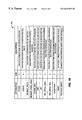
The pipe control unit 401 performs a number of operations in handling the instruction flow. An important feature of the pipe control unit 401 is the pipeline snapshot file 415 (shown in FIG. 4) implemented within pipe control unit 401. Snapshot file 415 may be implemented as a lookup table having a table entry 701 (shown in FIG. 7) corresponding to each execution stage in the pipeline. The snapshot file 415 provides a central resource for all pipeline control operations such as dependency checks, operand forwarding, exception handling, and the like. In a particular implementation, snapshot file 415 includes four entries corresponding to the three execution pipeline stages and the write back pipeline stage.
FIG. 7A and FIG. 7B show exemplary snapshot files 701 and 702 indicating entries holding metadata describing the instruction execution state at the corresponding pipe stage. As instructions move from one stage to another, their associated snapshot entry moves to the corresponding snapshot entry 701 or 702. The contents of each snapshot entry 701 may be varied to meet the needs of a particular application. The specific examples shown in FIG. 7 correspond to pipeline control operations described hereinbelow. The essential functionality of examples 701 and 702 are similar although the implementation of that essential functionality differs between the examples. In comparing the examples, snapshot file 701 does not include a “STAGE” entry as that is implied by the index of the entry whereas example 702 includes an explicit STAGE entry. The single STAGE_RDY entry of FIG. 7B is implemented using three separate entries (E1_RESULT, E2_RESULT and E3_RESULT) in the example of FIG. 7A. The fields have the function generally described in the figures and additional or fewer fields may be added to meet the needs of a particular application.
In operation, the snapshot register may be used by the pipeline control 401 to perform a number of parallel checks to classify the instruction currently being processed by the decoder 405. For example, the three potential operand register fields of the instruction word are checked against the existing pipe snapshot to detect data dependency, forwarding dependence, write-after-write hazard, and write-after-write for an accumulating-type instruction.
Data dependency checking is performed by comparing the operand register specifiers of the instruction in decode against the register destinations marked to be written by each subsequent pipeline stage. If there is a match and the data will not be ready in this stage then there is a true data dependency that is resolved by, for example, stalling the instruction currently within the decode stage. Similarly, forwarding dependency checking is performed by comparing Rdest to determine if the result upon which the decoder instruction depends will be ready in the matched stage (forward from the result bus) or a previous stage (implying forward from the pipefile).
A write-after-write hazard is indicated when an operand register specifier matches on more than one entry. In this case, the dependency can be resolved if the data can be forwarded from the correct (i.e., earlier) conflicting pipeline stage. Accordingly, pipe control can determine to control the forwarding from the earlier stage which matches. Using the same mechanism, the pipe control unit 401 can easily generate control for the internal forwarding of the IEU 305 by simply extending the metadata contained in snapshot files 701 and 702.
When there is an instruction of the IEU-internal forwarding class (e.g., an accumulating-type instruction) in the first or second execution stages 507 or 509, the register destination of this instruction is checked against the register destination of an earlier instruction in the third execution stage 511. If a match is found and the instruction in the third execution stage 511 is of the same class, the pipe control unit 401 will generate the proper internal forwarding select signals to forward the third stage result to the first or second stage 507 or 509.
For a hazard to actually be detected one of the source registers of the instruction must be valid and must match against a valid register destination in the snapshot file. Hazard detection of the preferred implementation only detects general purpose register dependencies. Though the snapshot file also stores control register destinations, these are not marked as valid and therefore do not show up in the dependency checks. However, alternative implementations could implement control checks using snapshot files 701 and 702 by adding one additional field.
Under normal conditions once an instruction has been issued to an execution unit its entry will progress through each stage of the snapshot file on each clock edge. At the beginning of each execution stage the control for writing the result to the pipefile is generated. This is determined by checking the E1_RESULT, E2_RESULT, and E3_RESULT fields of the current execution stage. For example, if E1_RESULT field is set for the instruction executing in the EXE_1 stage 507, the result from EXE_1 stage 507 will then be written into the pipefile entry indexed by the PIPE_FILE_ENTRY field. Similarly, the result from the EXE_2 and EXE_3 stages will be written into the pipefile 409 when the E2_RESULT and E3_RESULT fields of the corresponding snapshot file entries are set. The write into pipefile 409 will occur even if the EXCEPTION field in snapshot file 702 is set. This is to allow transportation data for exceptions back to the branch unit. Once an instruction reaches write-back, the rdest_valid field also determines if the contents of the pipefile is written back to the architectural register file. Once in write-back, if no exception has occurred, the instruction has completed.
An important feature of the present invention involves handling internal operand forwarding within the pipeline. Because the snapshot entry 701 indicates which pipe stage will produce a result to the pipefile 409, subsequent instructions can reliably use the interim result from the pipefile 409 before it is committed to architectural state. By enabling operand bypass between stages a significant percentage of data hazards can be avoided. This process is called internal operand forwarding.
When decode indicates that it has a valid instruction the pipe control block determines from the instruction code the source of the operands for the instruction. The present invention enables an operand can be sourced from, for example:
Register operands;
Indirectly forwarded operands through the three pipefile entries;
Directly forwarded operands from the result busses of the associated with the instruction execution pipe stages;
The extended immediate field from the instruction;
The program counter;
The contents of an instruction address register (IAR);
The contents of a control register; and
A tied low constant field;
The above gives up to 12 possible sources of input to some operand. FIG. 8 illustrates an exemplary operand multiplexing (“muxing”) mechanism that enables rich sharing of operands within the pipeline. The mechanism shown in FIG. 8 is distributed throughout pipe control unit 401 as described below. The operand multiplexor mechanism of FIG. 8 produces three choices (e.g., IFU_SRC1, IFU_SRC2, IFU_SRC3) for the source operands provided to the first execution stage 507. Each execution stage produces a result (labeled EXE_1, EXE_2, and EXE_3 in FIG. 8) that may be used as a source operand input to the first execution stage 507. Execution stage 507 is associated with a multiplexors 809 a-809 c for selecting up to three source operands from those available. The specific examples given herein are for purposes of explanation and understanding, and are not a limitation on the actual implementation.
It should also be understood that execution stage 507, 509 and 511 shown in FIG. 8 are representative of all of the hardware resources used in that execution stage as defined by the processor microarchitecture. An execution stage is physically implemented using the hardware resources such as those shown in FIG. 3. The outputs of multiplexors 809 are physically coupled to each of the hardware resources that will use the source operands during its operation.
The multiplexing of these operand sources in the particular example is distributed in the following way:
The program counter (PC), instruction address registers, and control register contents are pre-muxed in the branch unit using multiplexors 801 and 803. All these inputs are available at the start of the cycle.
The decode constant extracted from the instruction and possibly tied high zeroes are pre-muxed in the decode stage using multiplexor 811.
The outputs of the pipefile 409 are muxed with the program counter data and decode constant data respectively in multiplexors 805 and 813.
The register file contents are muxed with the pipefile outputs using multiplexors 807, 815, and 821 to produce source operands which are distributed down the execution datapath (IFU_SRC1, IFU_SRC2, IFU_SRC3 in FIG. 8).
Forwarding of completing results is done locally within the execution datapath. As the result is being driven back up the datapath from the various stages of execution (imu_result_exl,_ex2 and _ex3), the result taps back into the multiplexors 809 at the input to the execution sub-units. The result is also driven back up to the pipefile 409 for ultimate storage in the register file 407. Pipe control unit 401 controls the selection of the multiplexor 809 latches.
The LSU ex3 result is muxed with the output of the IEU ex3 result (from the multiplier). Internally IEU 305 multiplexes several results into the IEU_EXE3 result. In general, all results produced in pipe stage 511 are multiplexed onto EXE_3 result bus line. This is also controlled by the pipe control unit 401.
In this manner, pipe control unit 401 generates the control signals for multiplexors and execution stage resources. This enables the source operand inputs used by each execution stage to be selected from among a plurality of possible inputs. Of particular significance is that each source operand can be forwarded from the interim results stored in the pipefile if valid results are available in the pipefile. This is useful in handling data hazards in a manner that limits the need to stall the pipeline or fill the pipeline with bubbles while data dependencies resolve. The particular choice and distribution of operand sources can include more or fewer sources to meet the needs of a particular application and unless specified otherwise herein the examples are provided for example purposes only.
FIG. 9 schematically illustrates the execution stages of a pipeline and the operand sources for each stage. Each execution stage (EXE_1, EXE_2 and EXE_3) may generate a result. The specific stage that generates a result for any given instruction will vary from instruction-to-instruction, but is preferably indicated in the “stage_rdy” field of the snapshot file entry 702 or the E1_RESULT, E2_RESULT and E3_RESULT fields described hereinbefore. Each source operand can be taken from the execution unit's own result output. FIG. 9 shows an operand bus comprising IFU_SRCI, IFU_SRC2 and IFU_SRC3 (determined as shown in FIG. 8) and a results bus 906 comprising EXE_1_RESULT, EXE_2_RESULT and EXE_3_RESULT. The results bus 906 carries results to appropriate entries in pipefile 409.
In the embodiment shown in FIG. 9 each execution stage corresponds to a specific entry in the pipe file 409 (e.g., EXE_2 corresponds to pipefile entry 409A, EXE_3 stage 509 corresponds to entry 409B). Results are written from the result bus into pipefile 409 according to the “stage_rdy”value in the snapshot register (FIG. 7A) or the El RESULT through E3_RESULT entries (FIG. 7B) as described hereinbefore. Pipefile 409A takes the EXE_1 result and can forward its contents when the instruction that produces the result is in the EXE_2 stage. Similarly, pipefile entry 409B takes the EXE_2 result and 409C takes the EXE_3 result respectively. Otherwise, results are moved sequentially from entry 409A to 409B to 409C. Entry 409C corresponds to the write back pipe stage. Assuming the snapshot register entry 701 corresponding to the instruction in the write back stage is valid and does not indicate an exception, the value stored in pipefile stage 409 is copied to the appropriate register in register file 407.
Significantly, the operands for each execution stage can be selected from either the operand bus or the results bus. Hence, a result that is ready in EXE_1 will be driven onto the EXE_1_RESULT line and can be used as an operand on the following cycle in the second and third execution stages before being written to either register file 407 or the pipefile 409. Similarly, a result determined in EXE_3 can be used on the next clock cycle as an operand for an instruction executing in the first execution stage (EXE_1). This enables the instruction to be issued to EXE_1 without delays or pipeline bubbles normally associated with waiting for the EXE_3_RESULT to be written out to a register or rename register.
Furthermore, execution stage 507 can use its own output as well as the outputs of stages 509 and 511 as an operand for the next cycle. This is done, for example, by selecting EXE_1_RESULT, EXE_2_RESULT or EXE_3_RESULT as one of its operand inputs. This is particularly useful for accumulate-type operations where the destination register is used in a series of instructions to hold an accumulating result. Without this feature, pipeline bubbles would likely be inserted between accumulate instructions thereby reducing throughput significantly. Using this feature, the decoder can issue accumulating type instructions one-after-another.
The results are coupled to a corresponding selector unit 901. Each selector selectively couples the result to one of the result bus lines. Each selector is controlled by, for example, the pointer value (labeled POINTER_1, POINTER_2 and POINTER_3 in FIG. 9) corresponding to that pipe stage. The pointer values are determined from the PIPE_FILE_ENTRY and E1_RESULT, E2_RESULT and E3_RESULT fields of snapshot entry 701. Alternatively, the pointer value 903 may be stored in the snapshot file entry 701 as described hereinbefore, or may be stored in a separate register that operates in a manner such that the pointer value remains associated with a particular instruction as the instruction moves through the pipeline. The result is written to the specified pipefile entry 409 a-409 c.
Pipefile 409 preferably comprises dual ported memory structure so that the contents of any entry 409 a-409 c can be written to and/or read out at any time. The memory within pipefile 409 is typically implemented using CMOS or BiCMOS static random access memory (SRAM) technology using four or more transistors per stored bit. A multiplexor set 903 selectively couples the data stored in pipefile entries 409 a-409 c to appropriate lines on a pipefile bus 904. The pipefile bus 904 provides values to the multiplexing mechanism shown in FIG. 8, for example. Multiplexor set 903 is controlled by pipe control unit 401 to couple appropriate bus lines to corresponding entries 409 a-409 c in pipefile 409.
As a particular example, assume an instruction that generates its result in EXE_1 and the pointer values are set such that the EXE_1 result is written to pipefile entry 409 b. From pipefile entry 409 b the result can be multiplexed, onto any of the IFU_SRC lines by appropriate settings in multiplexor set 903. On the next pipe cycle, the example instruction will move to pipe stage EXE_2, while pipefile entry 409 b remains unchanged. In this manner, a result needs only be written to the results bus one time while remaining continuously available for forwarding while the instruction remains in the pipeline the hundreds of transistors used to store the value in entry 409 b do not have to be switched until after the value is written back and the pipe file entry is reassigned to an instruction in the decoder.
It is contemplated that the functionality of multiplexor 903 may be implemented in a variety of ways depending on the level of operand forwarding needed in a particular implementation. For example, if operand forwarding from the pipefile is not needed, there would be no corresponding need to generate the PIPEFILE_SCR1, PIPEFILE_SCR2 and PIPEFILE_SCR3 lines. The writeback line is controlled by the writeback stage pointer and selects one of the pipefile entries for writeback to an architectural register in register file 407.
A particular example involves execution of accumulate type instructions. Consider a series of instructions such as:
MAC a, b, x
MAC c, d, x
MAC e, f, x
where MAC is a “multiply accumulate” instruction that computes the multiple of the first and second operands and accumulates the product with a value stored in a third specified register. Prior implementations would force the MAC c, d, x instruction to wait until the first MAC instruction completed so that the accumulate register (x in the example) is stored in a register or rename register. However, in the present invention, the decode unit is aware that the MAC c, d, x instruction will not need the x register value until the third pipestage. By enabling the third pipestage to accept its own result as an input for the next instruction in that pipestage, the x register value will be immediately available to the subsequent instructions. Hence, the MAC instructions can be streamed one after the other into the pipeline without bubbles.
While the invention has been particularly shown and described with reference to a preferred embodiment thereof, it will be understood by those skills in the art that various other changes in the form and details may be made without departing from the spirit and scope of the invention. The various embodiments have been described using hardware examples, but the present invention can be readily implemented in software. For example, it is contemplated that a programmable logic device, hardware emulator, software simulator, or the like of sufficient complexity could implement the present invention as a computer program product including a computer usable medium having computer readable code embodied therein to perform precise architectural update in an emulated or simulated out-of-order machine. Accordingly, these and other variations are equivalent to the specific implementations and embodiments described herein.

Claims (24)

What is claimed is:
1. A method for forwarding data within a pipeline of a pipelined data processor comprising the steps of:
providing a plurality of execution pipeline stages where each stage accepts a plurality of operand inputs and generates a result;
copying the results generated by each execution pipeline stage to an entry of a single pipefile, the entry corresponding to the execution pipeline stage; and
selectively coupling the result generated by each execution pipeline stage to an operand input of one of the execution pipeline stages.
2. The method of claim 1 wherein the selectively coupling comprises coupling the result generated by a specific one of the execution pipeline stages to an operand input of the same execution pipeline stage.
3. The method of claim 1 wherein the selectively coupling comprises coupling the result generated by a first of the execution pipeline stages to an operand input of a second of the execution pipeline stage.
4. The method of claim 1, wherein the step of selectively coupling is performed substantially simultaneously with the step of copying.
5. The method of claim 4 wherein the step of selectively coupling is performed so as-to make the selectively coupled result available as an operand input before pipefile entry to which the result is being copied is valid.
6. A data processor comprising:
a plurality of execution pipeline stages where each stage accepts a plurality of operand inputs and generates a result;
a results bus directly distributing the generated results from each of the execution pipeline stages throughout the plurality of pipeline stages;
a pipefile coupled to the results bus to selectively receive the generated results; and
a multiplexor associated with each execution pipeline stage operative to selectively couple the results bus to an operand input of the associated execution pipeline stages.
7. The data processor of claim 6 wherein the multiplexor is operative to selectively couple the result of each of the execution pipeline stages to an operand input of the execution pipeline stage generating the result.
8. The data processor of claim 6 wherein the multiplexor is operative to selectively couple the result of a first of the execution pipeline stages to an operand input of a second of the execution pipeline stages.
9. The data processor of claim 6 further comprising:
a pipefile coupled to the results bus and operative to store the data on the result bus at substantially the same time that the multiplexor selectively couples the result bus to an operand input.
10. A method of forwarding data between multiple execution stages forming an execution pipeline of a data processor, comprising the steps of:
applying multiple operands of an instruction to the execution pipeline to produce a result from each of the multiple execution stages;
each of the multiple execution stages producing a result;
selectively coupling the result from each of the multiple execution stages to an entry of a pipefile corresponding to such execution stage;
selectively coupling the result from each of the multiple execution stages to a register in a general register file; and
selectively coupling an entry of the pipefile and a register in the general register file to a first one of the multiple execution stages of the execution pipeline.
11. The method of claim 10, wherein the entry coupled to the first execution stage of the execution pipeline is an operand.
12. The method of claim 10, the coupling step including the step of writing the result to a snapshot register.
13. A method of forwarding data between multiple execution stages forming an execution pipeline of a data processor, comprising the steps of:
providing multiple operands to the execution pipeline for performing an operation whereby each of the multiple execution stages produces a result;
copying the result produced by each of the multiple execution stages to a corresponding entry of a single pipefile; and
selectively coupling the content of the single pipefile to each of the multiple execution stages.
14. The method of claim 13, wherein the multiple execution stages includes an input execution stage for receiving the multiple operands, and including coupling the result produced by each of the other of the multiple execution stages to the input execution stage.
15. A data processor, including:
an execution pipeline, comprising a plurality of execution stages, including a first execution stage, coupled to receive operands of an instruction for performing operations dictated by said instruction;
a single pipefile coupled to receive output from the execution stages; and
a memory coupled via the pipefile to each of the plurality of execution stages for receiving and storing a result at a memory entry corresponding to such execution stage.
16. The data processor of claim 15, including a selector operating to forward a selected one of the memory entries to the first execution stage of the execution pipeline.
17. The data processor of claim 15, including a selector operating to forward a selected one of the memory entries to a one of the plurality of execution stages of the execution pipeline.
18. The data processor of claim 15, including a snapshot register for receiving and storing instruction decode and execution information.
19. The data processor of claim 18, wherein the instruction execution information includes criteria for selecting a source operands received by the execution pipeline.
20. An execution pipeline of a data processor, including
a plurality of serial connected pipeline execution stages, including an input pipeline execution stage that receives one or more operands for performing an operation, each of the plurality of pipeline execution stages having a result output directly coupled to an input of each of the other of the plurality of pipeline execution stages, each result output further selectively coupled to a pipefile.
21. The execution pipeline of claim 20, wherein the result output of each of the plurality of pipeline execution stages is coupled to an input of the input pipeline execution stage.
22. The execution pipeline of claim 20, including a pipefile having at least one pipefile entry for each of the plurality of pipeline execution stages, the result output of each pipeline execution stage being coupled to a corresponding pipefile entry, each corresponding pipefile entry being coupled to an input of each of the pipeline execution stages.
23. A method of forwarding result data between a plurality of serial connected execution stages of an execution pipeline of a data processor, including the steps of:
providing one or more operands to a first one of the plurality of execution stages, the each execution stages operating to perform an operation and to produce a result;
selectively coupling the result produced by each execution stage to a corresponding entry of a pipefile and to a register of a register file for storage; and
selectively coupling an entry of the pipefile and a register of the register file to an input of each of the execution stages.
24. The method of claim 23, including the step of coupling the result produced by each execution stage to the first one of the plurality of execution stages.
US09/411,431 1999-10-01 1999-10-01 Mechanism for forward data in a processor pipeline using a single pipefile connected to the pipeline Expired - Fee Related US6633971B2 (en)

Priority Applications (2)

Application Number Priority Date Filing Date Title
US09/411,431 US6633971B2 (en) 1999-10-01 1999-10-01 Mechanism for forward data in a processor pipeline using a single pipefile connected to the pipeline
JP2000286977A JP2001142699A (en) 1999-10-01 2000-09-21 Transfer mechanism of instruction data in pipeline processor

Applications Claiming Priority (1)

Application Number Priority Date Filing Date Title
US09/411,431 US6633971B2 (en) 1999-10-01 1999-10-01 Mechanism for forward data in a processor pipeline using a single pipefile connected to the pipeline

Publications (2)

Publication Number Publication Date
US20030154364A1 US20030154364A1 (en) 2003-08-14
US6633971B2 true US6633971B2 (en) 2003-10-14

Family

ID=23628898

Family Applications (1)

Application Number Title Priority Date Filing Date
US09/411,431 Expired - Fee Related US6633971B2 (en) 1999-10-01 1999-10-01 Mechanism for forward data in a processor pipeline using a single pipefile connected to the pipeline

Country Status (2)

Country Link
US (1) US6633971B2 (en)
JP (1) JP2001142699A (en)

Cited By (10)

* Cited by examiner, † Cited by third party
Publication number Priority date Publication date Assignee Title
US20020124155A1 (en) * 2000-10-17 2002-09-05 Stmicroelectronics S.R.L. Processor architecture
US20050071830A1 (en) * 2003-09-30 2005-03-31 Starcore, Llc Method and system for processing a sequence of instructions
US20060149930A1 (en) * 2004-12-08 2006-07-06 Hiroaki Murakami Systems and methods for improving performance of a forwarding mechanism in a pipelined processor
US20060168393A1 (en) * 2005-01-27 2006-07-27 Christensen Bjorn P Apparatus and method for dependency tracking and register file bypass controls using a scannable register file
US20070174592A1 (en) * 2006-01-20 2007-07-26 Dieffenderfer James N Early conditional selection of an operand
US20110238962A1 (en) * 2010-03-23 2011-09-29 International Business Machines Corporation Register Checkpointing for Speculative Modes of Execution in Out-of-Order Processors
US20120042153A1 (en) * 2010-08-13 2012-02-16 Morrison Gary R Data processing system having temporal redundancy and method therefor
US20140129805A1 (en) * 2012-11-08 2014-05-08 Nvidia Corporation Execution pipeline power reduction
US20140215189A1 (en) * 2013-01-29 2014-07-31 Arm Limited Data processing apparatus and method for controlling use of an issue queue
US20150074380A1 (en) * 2013-09-06 2015-03-12 Futurewei Technologies Inc. Method and apparatus for asynchronous processor pipeline and bypass passing

Families Citing this family (4)

* Cited by examiner, † Cited by third party
Publication number Priority date Publication date Assignee Title
US8078845B2 (en) * 2005-12-16 2011-12-13 Freescale Semiconductor, Inc. Device and method for processing instructions based on masked register group size information
US7996655B2 (en) * 2008-04-22 2011-08-09 International Business Machines Corporation Multiport execution target delay queue FIFO array
US10338925B2 (en) 2017-05-24 2019-07-02 Microsoft Technology Licensing, Llc Tensor register files
US10372456B2 (en) 2017-05-24 2019-08-06 Microsoft Technology Licensing, Llc Tensor processor instruction set architecture

Citations (75)

* Cited by examiner, † Cited by third party
Publication number Priority date Publication date Assignee Title
US4112489A (en) * 1976-02-06 1978-09-05 International Computers Limited Data processing systems
EP0165600A2 (en) 1984-06-20 1985-12-27 Convex Computer Corporation Input/output bus for computer
US4644466A (en) * 1983-12-05 1987-02-17 Nec Corporation Pipeline processor
US4814981A (en) 1986-09-18 1989-03-21 Digital Equipment Corporation Cache invalidate protocol for digital data processing system
US5251311A (en) 1989-10-12 1993-10-05 Nec Corporation Method and apparatus for processing information and providing cache invalidation information
US5386565A (en) 1990-01-23 1995-01-31 Hitachi, Ltd. Method and system for controlling/monitoring computer system having plural operating systems to run thereon
EP0636976A1 (en) 1993-07-28 1995-02-01 Koninklijke Philips Electronics N.V. Microcontroller provided with hardware for supporting debugging as based on boundary scan standard-type extensions
EP0652516A1 (en) 1993-11-03 1995-05-10 Advanced Micro Devices, Inc. Integrated microprocessor
US5423050A (en) 1991-11-27 1995-06-06 Ncr Corporation Intermodule test across system bus utilizing serial test bus
US5434804A (en) 1993-12-29 1995-07-18 Intel Corporation Method and apparatus for synchronizing a JTAG test control signal to an on-chip clock signal
US5440705A (en) 1986-03-04 1995-08-08 Advanced Micro Devices, Inc. Address modulo adjust unit for a memory management unit for monolithic digital signal processor
US5448576A (en) 1992-10-29 1995-09-05 Bull Hn Information Systems Inc. Boundary scan architecture extension
US5452432A (en) 1990-08-14 1995-09-19 Chips And Technologies, Inc. Partially resettable, segmented DMA counter
US5455936A (en) 1993-04-28 1995-10-03 Nec Corporation Debugger operable with only background monitor
US5467476A (en) * 1991-04-30 1995-11-14 Kabushiki Kaisha Toshiba Superscalar processor having bypass circuit for directly transferring result of instruction execution between pipelines without being written to register file
US5479652A (en) 1992-04-27 1995-12-26 Intel Corporation Microprocessor with an external command mode for diagnosis and debugging
US5483518A (en) 1992-06-17 1996-01-09 Texas Instruments Incorporated Addressable shadow port and protocol for serial bus networks
US5488688A (en) 1994-03-30 1996-01-30 Motorola, Inc. Data processor with real-time diagnostic capability
EP0702239A2 (en) 1994-09-01 1996-03-20 STMicroelectronics Limited A controller for implementing scan testing
US5530965A (en) 1992-11-06 1996-06-25 Hitachi, Ltd. Multiply connectable microprocessor and microprocessor system
EP0720092A1 (en) 1994-12-28 1996-07-03 Hewlett-Packard Company Microprocessor with debugging system
US5570375A (en) 1995-05-10 1996-10-29 National Science Council Of R.O.C. IEEE Std. 1149.1 boundary scan circuit capable of built-in self-testing
JPH08320796A (en) 1994-09-09 1996-12-03 Hitachi Ltd Data processor
JPH08329687A (en) 1995-06-05 1996-12-13 Hitachi Ltd Semiconductor integrated circuit
US5596734A (en) 1993-12-17 1997-01-21 Intel Corporation Method and apparatus for programming embedded memories of a variety of integrated circuits using the IEEE test access port
US5598551A (en) 1993-07-16 1997-01-28 Unisys Corporation Cache invalidation sequence system utilizing odd and even invalidation queues with shorter invalidation cycles
US5608881A (en) 1992-11-06 1997-03-04 Hitachi, Ltd. Microcomputer system for accessing hierarchical buses
US5613153A (en) 1994-10-03 1997-03-18 International Business Machines Corporation Coherency and synchronization mechanisms for I/O channel controllers in a data processing system
US5627842A (en) 1993-01-21 1997-05-06 Digital Equipment Corporation Architecture for system-wide standardized intra-module and inter-module fault testing
US5657273A (en) 1994-11-22 1997-08-12 Hitachi, Ltd. Semiconductor device capable of concurrently transferring data over read paths and write paths to a memory cell array
JPH09212358A (en) 1996-01-31 1997-08-15 Hitachi Ltd Data processor and microprocessor
US5682545A (en) 1991-06-24 1997-10-28 Hitachi, Ltd. Microcomputer having 16 bit fixed length instruction format
JPH09311786A (en) 1996-03-18 1997-12-02 Hitachi Ltd Data processor
US5704034A (en) 1995-08-30 1997-12-30 Motorola, Inc. Method and circuit for initializing a data processing system
US5708773A (en) 1995-07-20 1998-01-13 Unisys Corporation JTAG interface system for communicating with compliant and non-compliant JTAG devices
US5724549A (en) 1992-04-06 1998-03-03 Cyrix Corporation Cache coherency without bus master arbitration signals
WO1998013759A1 (en) 1996-09-27 1998-04-02 Hitachi, Ltd. Data processor and data processing system
US5737516A (en) 1995-08-30 1998-04-07 Motorola, Inc. Data processing system for performing a debug function and method therefor
JPH10106269A (en) 1996-08-06 1998-04-24 Hitachi Ltd Semiconductor memory, semiconductor device, data-processing device, and computer system
US5751621A (en) 1994-11-17 1998-05-12 Hitachi, Ltd. Multiply-add unit and data processing apparatus using it
JPH10124484A (en) 1996-10-16 1998-05-15 Hitachi Ltd Data processor and data processing system
US5768152A (en) 1996-08-28 1998-06-16 International Business Machines Corp. Performance monitoring through JTAG 1149.1 interface
US5771240A (en) 1996-11-14 1998-06-23 Hewlett-Packard Company Test systems for obtaining a sample-on-the-fly event trace for an integrated circuit with an integrated debug trigger apparatus and an external pulse pin
JPH10177520A (en) 1996-10-16 1998-06-30 Hitachi Ltd Data processor and data processing system
US5774701A (en) 1995-07-10 1998-06-30 Hitachi, Ltd. Microprocessor operating at high and low clok frequencies
US5778237A (en) 1995-01-10 1998-07-07 Hitachi, Ltd. Data processor and single-chip microcomputer with changing clock frequency and operating voltage
US5781558A (en) 1996-08-14 1998-07-14 International Computers Limited Diagnostic memory access
US5790880A (en) * 1996-01-04 1998-08-04 Advanced Micro Devices Microprocessor configured to dynamically connect processing elements according to data dependencies
US5796978A (en) 1994-09-09 1998-08-18 Hitachi, Ltd. Data processor having an address translation buffer operable with variable page sizes
US5805852A (en) * 1996-05-13 1998-09-08 Mitsubishi Denki Kabushiki Kaisha Parallel processor performing bypass control by grasping portions in which instructions exist
US5828825A (en) 1993-12-22 1998-10-27 Intel Corporation Method and apparatus for pseudo-direct access to embedded memories of a micro-controller integrated circuit via the IEEE test access port
US5832248A (en) 1992-11-06 1998-11-03 Hitachi, Ltd. Semiconductor integrated circuit having CPU and multiplier
US5835963A (en) 1994-09-09 1998-11-10 Hitachi, Ltd. Processor with an addressable address translation buffer operative in associative and non-associative modes
US5848247A (en) 1994-09-13 1998-12-08 Hitachi, Ltd. Microprocessor having PC card interface
US5860127A (en) 1995-06-01 1999-01-12 Hitachi, Ltd. Cache memory employing dynamically controlled data array start timing and a microcomputer using the same
US5862387A (en) 1995-04-21 1999-01-19 Intel Corporation Method and apparatus for handling bus master and direct memory access (DMA) requests at an I/O controller
US5867726A (en) 1995-05-02 1999-02-02 Hitachi, Ltd. Microcomputer
US5884092A (en) 1995-10-09 1999-03-16 Hitachi, Ltd. System for maintaining fixed-point data alignment within a combination CPU and DSP system
US5896550A (en) 1997-04-03 1999-04-20 Vlsi Technology, Inc. Direct memory access controller with full read/write capability
US5918045A (en) 1996-10-18 1999-06-29 Hitachi, Ltd. Data processor and data processing system
US5930523A (en) 1993-09-17 1999-07-27 Hitachi Ltd. Microcomputer having multiple bus structure coupling CPU to other processing elements
US5930833A (en) 1994-04-19 1999-07-27 Hitachi, Ltd. Logical cache memory storing logical and physical address information for resolving synonym problems
EP0933926A1 (en) 1998-01-30 1999-08-04 STMicroelectronics Limited DMA controller
US5944841A (en) 1997-04-15 1999-08-31 Advanced Micro Devices, Inc. Microprocessor with built-in instruction tracing capability
US5950012A (en) 1996-03-08 1999-09-07 Texas Instruments Incorporated Single chip microprocessor circuits, systems, and methods for self-loading patch micro-operation codes and patch microinstruction codes
US5953538A (en) 1996-11-12 1999-09-14 Digital Equipment Corporation Method and apparatus providing DMA transfers between devices coupled to different host bus bridges
US5956477A (en) 1996-11-25 1999-09-21 Hewlett-Packard Company Method for processing information in a microprocessor to facilitate debug and performance monitoring
EP0945805A1 (en) 1998-03-23 1999-09-29 STMicroelectronics Limited A cache coherency mechanism
US5978902A (en) 1997-04-08 1999-11-02 Advanced Micro Devices, Inc. Debug interface including operating system access of a serial/parallel debug port
US5978874A (en) 1996-07-01 1999-11-02 Sun Microsystems, Inc. Implementing snooping on a split-transaction computer system bus
US5983017A (en) 1996-11-12 1999-11-09 Lsi Logic Corporation Virtual monitor debugging method and apparatus
US5983379A (en) 1996-10-31 1999-11-09 Sgs-Thomson Microelectronics Limited Test access port controller and a method of effecting communication using the same
EP0959411A1 (en) 1998-04-29 1999-11-24 STMicroelectronics Limited Packet distribution in a microcomputer
US5996065A (en) * 1997-03-31 1999-11-30 Intel Corporation Apparatus for bypassing intermediate results from a pipelined floating point unit to multiple successive instructions
US6351805B2 (en) * 1998-09-30 2002-02-26 Intel Corporation Non-stalling circular counterflow pipeline processor with reorder buffer

Patent Citations (78)

* Cited by examiner, † Cited by third party
Publication number Priority date Publication date Assignee Title
US4112489A (en) * 1976-02-06 1978-09-05 International Computers Limited Data processing systems
US4644466A (en) * 1983-12-05 1987-02-17 Nec Corporation Pipeline processor
EP0165600A2 (en) 1984-06-20 1985-12-27 Convex Computer Corporation Input/output bus for computer
US5440705A (en) 1986-03-04 1995-08-08 Advanced Micro Devices, Inc. Address modulo adjust unit for a memory management unit for monolithic digital signal processor
US4814981A (en) 1986-09-18 1989-03-21 Digital Equipment Corporation Cache invalidate protocol for digital data processing system
US5251311A (en) 1989-10-12 1993-10-05 Nec Corporation Method and apparatus for processing information and providing cache invalidation information
US5386565A (en) 1990-01-23 1995-01-31 Hitachi, Ltd. Method and system for controlling/monitoring computer system having plural operating systems to run thereon
US5452432A (en) 1990-08-14 1995-09-19 Chips And Technologies, Inc. Partially resettable, segmented DMA counter
US5467476A (en) * 1991-04-30 1995-11-14 Kabushiki Kaisha Toshiba Superscalar processor having bypass circuit for directly transferring result of instruction execution between pipelines without being written to register file
US5682545A (en) 1991-06-24 1997-10-28 Hitachi, Ltd. Microcomputer having 16 bit fixed length instruction format
US5423050A (en) 1991-11-27 1995-06-06 Ncr Corporation Intermodule test across system bus utilizing serial test bus
US5724549A (en) 1992-04-06 1998-03-03 Cyrix Corporation Cache coherency without bus master arbitration signals
US5479652B1 (en) 1992-04-27 2000-05-02 Intel Corp Microprocessor with an external command mode for diagnosis and debugging
US5479652A (en) 1992-04-27 1995-12-26 Intel Corporation Microprocessor with an external command mode for diagnosis and debugging
US5483518A (en) 1992-06-17 1996-01-09 Texas Instruments Incorporated Addressable shadow port and protocol for serial bus networks
US5448576A (en) 1992-10-29 1995-09-05 Bull Hn Information Systems Inc. Boundary scan architecture extension
US5608881A (en) 1992-11-06 1997-03-04 Hitachi, Ltd. Microcomputer system for accessing hierarchical buses
US5530965A (en) 1992-11-06 1996-06-25 Hitachi, Ltd. Multiply connectable microprocessor and microprocessor system
US5832248A (en) 1992-11-06 1998-11-03 Hitachi, Ltd. Semiconductor integrated circuit having CPU and multiplier
US5627842A (en) 1993-01-21 1997-05-06 Digital Equipment Corporation Architecture for system-wide standardized intra-module and inter-module fault testing
US5455936A (en) 1993-04-28 1995-10-03 Nec Corporation Debugger operable with only background monitor
US5598551A (en) 1993-07-16 1997-01-28 Unisys Corporation Cache invalidation sequence system utilizing odd and even invalidation queues with shorter invalidation cycles
US5590354A (en) 1993-07-28 1996-12-31 U.S. Philips Corporation Microcontroller provided with hardware for supporting debugging as based on boundary scan standard-type extensions
EP0636976A1 (en) 1993-07-28 1995-02-01 Koninklijke Philips Electronics N.V. Microcontroller provided with hardware for supporting debugging as based on boundary scan standard-type extensions
US5930523A (en) 1993-09-17 1999-07-27 Hitachi Ltd. Microcomputer having multiple bus structure coupling CPU to other processing elements
EP0652516A1 (en) 1993-11-03 1995-05-10 Advanced Micro Devices, Inc. Integrated microprocessor
US5596734A (en) 1993-12-17 1997-01-21 Intel Corporation Method and apparatus for programming embedded memories of a variety of integrated circuits using the IEEE test access port
US5828825A (en) 1993-12-22 1998-10-27 Intel Corporation Method and apparatus for pseudo-direct access to embedded memories of a micro-controller integrated circuit via the IEEE test access port
US5434804A (en) 1993-12-29 1995-07-18 Intel Corporation Method and apparatus for synchronizing a JTAG test control signal to an on-chip clock signal
US5488688A (en) 1994-03-30 1996-01-30 Motorola, Inc. Data processor with real-time diagnostic capability
US5930833A (en) 1994-04-19 1999-07-27 Hitachi, Ltd. Logical cache memory storing logical and physical address information for resolving synonym problems
EP0702239A2 (en) 1994-09-01 1996-03-20 STMicroelectronics Limited A controller for implementing scan testing
JPH08320796A (en) 1994-09-09 1996-12-03 Hitachi Ltd Data processor
US5796978A (en) 1994-09-09 1998-08-18 Hitachi, Ltd. Data processor having an address translation buffer operable with variable page sizes
US5835963A (en) 1994-09-09 1998-11-10 Hitachi, Ltd. Processor with an addressable address translation buffer operative in associative and non-associative modes
US5848247A (en) 1994-09-13 1998-12-08 Hitachi, Ltd. Microprocessor having PC card interface
US5613153A (en) 1994-10-03 1997-03-18 International Business Machines Corporation Coherency and synchronization mechanisms for I/O channel controllers in a data processing system
US5751621A (en) 1994-11-17 1998-05-12 Hitachi, Ltd. Multiply-add unit and data processing apparatus using it
US5657273A (en) 1994-11-22 1997-08-12 Hitachi, Ltd. Semiconductor device capable of concurrently transferring data over read paths and write paths to a memory cell array
EP0720092A1 (en) 1994-12-28 1996-07-03 Hewlett-Packard Company Microprocessor with debugging system
US5778237A (en) 1995-01-10 1998-07-07 Hitachi, Ltd. Data processor and single-chip microcomputer with changing clock frequency and operating voltage
US5862387A (en) 1995-04-21 1999-01-19 Intel Corporation Method and apparatus for handling bus master and direct memory access (DMA) requests at an I/O controller
US5867726A (en) 1995-05-02 1999-02-02 Hitachi, Ltd. Microcomputer
US5570375A (en) 1995-05-10 1996-10-29 National Science Council Of R.O.C. IEEE Std. 1149.1 boundary scan circuit capable of built-in self-testing
US5860127A (en) 1995-06-01 1999-01-12 Hitachi, Ltd. Cache memory employing dynamically controlled data array start timing and a microcomputer using the same
JPH08329687A (en) 1995-06-05 1996-12-13 Hitachi Ltd Semiconductor integrated circuit
US5774701A (en) 1995-07-10 1998-06-30 Hitachi, Ltd. Microprocessor operating at high and low clok frequencies
US5708773A (en) 1995-07-20 1998-01-13 Unisys Corporation JTAG interface system for communicating with compliant and non-compliant JTAG devices
US5737516A (en) 1995-08-30 1998-04-07 Motorola, Inc. Data processing system for performing a debug function and method therefor
US5704034A (en) 1995-08-30 1997-12-30 Motorola, Inc. Method and circuit for initializing a data processing system
US5884092A (en) 1995-10-09 1999-03-16 Hitachi, Ltd. System for maintaining fixed-point data alignment within a combination CPU and DSP system
US5790880A (en) * 1996-01-04 1998-08-04 Advanced Micro Devices Microprocessor configured to dynamically connect processing elements according to data dependencies
JPH09212358A (en) 1996-01-31 1997-08-15 Hitachi Ltd Data processor and microprocessor
US5950012A (en) 1996-03-08 1999-09-07 Texas Instruments Incorporated Single chip microprocessor circuits, systems, and methods for self-loading patch micro-operation codes and patch microinstruction codes
JPH09311786A (en) 1996-03-18 1997-12-02 Hitachi Ltd Data processor
US5805852A (en) * 1996-05-13 1998-09-08 Mitsubishi Denki Kabushiki Kaisha Parallel processor performing bypass control by grasping portions in which instructions exist
US5978874A (en) 1996-07-01 1999-11-02 Sun Microsystems, Inc. Implementing snooping on a split-transaction computer system bus
JPH10106269A (en) 1996-08-06 1998-04-24 Hitachi Ltd Semiconductor memory, semiconductor device, data-processing device, and computer system
SG55356A1 (en) 1996-08-06 1998-12-21 Hitachi Ltd Semiconductor memory apparatus semiconductor apparatus data processing apparatus and computer system
US5781558A (en) 1996-08-14 1998-07-14 International Computers Limited Diagnostic memory access
US5768152A (en) 1996-08-28 1998-06-16 International Business Machines Corp. Performance monitoring through JTAG 1149.1 interface
WO1998013759A1 (en) 1996-09-27 1998-04-02 Hitachi, Ltd. Data processor and data processing system
JPH10177520A (en) 1996-10-16 1998-06-30 Hitachi Ltd Data processor and data processing system
JPH10124484A (en) 1996-10-16 1998-05-15 Hitachi Ltd Data processor and data processing system
US5918045A (en) 1996-10-18 1999-06-29 Hitachi, Ltd. Data processor and data processing system
US5983379A (en) 1996-10-31 1999-11-09 Sgs-Thomson Microelectronics Limited Test access port controller and a method of effecting communication using the same
US5953538A (en) 1996-11-12 1999-09-14 Digital Equipment Corporation Method and apparatus providing DMA transfers between devices coupled to different host bus bridges
US5983017A (en) 1996-11-12 1999-11-09 Lsi Logic Corporation Virtual monitor debugging method and apparatus
US5771240A (en) 1996-11-14 1998-06-23 Hewlett-Packard Company Test systems for obtaining a sample-on-the-fly event trace for an integrated circuit with an integrated debug trigger apparatus and an external pulse pin
US5956477A (en) 1996-11-25 1999-09-21 Hewlett-Packard Company Method for processing information in a microprocessor to facilitate debug and performance monitoring
US5996065A (en) * 1997-03-31 1999-11-30 Intel Corporation Apparatus for bypassing intermediate results from a pipelined floating point unit to multiple successive instructions
US5896550A (en) 1997-04-03 1999-04-20 Vlsi Technology, Inc. Direct memory access controller with full read/write capability
US5978902A (en) 1997-04-08 1999-11-02 Advanced Micro Devices, Inc. Debug interface including operating system access of a serial/parallel debug port
US5944841A (en) 1997-04-15 1999-08-31 Advanced Micro Devices, Inc. Microprocessor with built-in instruction tracing capability
EP0933926A1 (en) 1998-01-30 1999-08-04 STMicroelectronics Limited DMA controller
EP0945805A1 (en) 1998-03-23 1999-09-29 STMicroelectronics Limited A cache coherency mechanism
EP0959411A1 (en) 1998-04-29 1999-11-24 STMicroelectronics Limited Packet distribution in a microcomputer
US6351805B2 (en) * 1998-09-30 2002-02-26 Intel Corporation Non-stalling circular counterflow pipeline processor with reorder buffer

Non-Patent Citations (2)

* Cited by examiner, † Cited by third party
Title
Richard York; Real Time Debug for System-on-Chip Devices; Jun. 1999; pp.1-6.
Richard York; Real Time Debug for System-on-Chip Devices; Jun. 1999; pp.1-6.</STEXT>

Cited By (21)

* Cited by examiner, † Cited by third party
Publication number Priority date Publication date Assignee Title
US6889317B2 (en) * 2000-10-17 2005-05-03 Stmicroelectronics S.R.L. Processor architecture
US20020124155A1 (en) * 2000-10-17 2002-09-05 Stmicroelectronics S.R.L. Processor architecture
US20050071830A1 (en) * 2003-09-30 2005-03-31 Starcore, Llc Method and system for processing a sequence of instructions
WO2005033873A2 (en) * 2003-09-30 2005-04-14 Starcore, Llc Method and system for processing a sequence of instructions
WO2005033873A3 (en) * 2003-09-30 2006-11-02 Starcore Llc Method and system for processing a sequence of instructions
US20060149930A1 (en) * 2004-12-08 2006-07-06 Hiroaki Murakami Systems and methods for improving performance of a forwarding mechanism in a pipelined processor
US20060168393A1 (en) * 2005-01-27 2006-07-27 Christensen Bjorn P Apparatus and method for dependency tracking and register file bypass controls using a scannable register file
US9710269B2 (en) * 2006-01-20 2017-07-18 Qualcomm Incorporated Early conditional selection of an operand
US20070174592A1 (en) * 2006-01-20 2007-07-26 Dieffenderfer James N Early conditional selection of an operand
CN101371223A (en) * 2006-01-20 2009-02-18 高通股份有限公司 Early conditional selection of an operand
US20110238962A1 (en) * 2010-03-23 2011-09-29 International Business Machines Corporation Register Checkpointing for Speculative Modes of Execution in Out-of-Order Processors
US20120042153A1 (en) * 2010-08-13 2012-02-16 Morrison Gary R Data processing system having temporal redundancy and method therefor
US9361104B2 (en) * 2010-08-13 2016-06-07 Freescale Semiconductor, Inc. Systems and methods for determining instruction execution error by comparing an operand of a reference instruction to a result of a subsequent cross-check instruction
US20140129805A1 (en) * 2012-11-08 2014-05-08 Nvidia Corporation Execution pipeline power reduction
US20140215189A1 (en) * 2013-01-29 2014-07-31 Arm Limited Data processing apparatus and method for controlling use of an issue queue
US9424045B2 (en) * 2013-01-29 2016-08-23 Arm Limited Data processing apparatus and method for controlling use of an issue queue to represent an instruction suitable for execution by a wide operand execution unit
US20150074380A1 (en) * 2013-09-06 2015-03-12 Futurewei Technologies Inc. Method and apparatus for asynchronous processor pipeline and bypass passing
US9606801B2 (en) 2013-09-06 2017-03-28 Huawei Technologies Co., Ltd. Method and apparatus for asynchronous processor based on clock delay adjustment
US9740487B2 (en) 2013-09-06 2017-08-22 Huawei Technologies Co., Ltd. Method and apparatus for asynchronous processor removal of meta-stability
US9846581B2 (en) * 2013-09-06 2017-12-19 Huawei Technologies Co., Ltd. Method and apparatus for asynchronous processor pipeline and bypass passing
US10042641B2 (en) 2013-09-06 2018-08-07 Huawei Technologies Co., Ltd. Method and apparatus for asynchronous processor with auxiliary asynchronous vector processor

Also Published As

Publication number Publication date
US20030154364A1 (en) 2003-08-14
JP2001142699A (en) 2001-05-25

Similar Documents

Publication Publication Date Title
US8069340B2 (en) Microprocessor with microarchitecture for efficiently executing read/modify/write memory operand instructions
US5150469A (en) System and method for processor pipeline control by selective signal deassertion
US5958041A (en) Latency prediction in a pipelined microarchitecture
US6279100B1 (en) Local stall control method and structure in a microprocessor
JP3548132B2 (en) Method and apparatus for flushing pipeline stages in a multithreaded processor
US5974523A (en) Mechanism for efficiently overlapping multiple operand types in a microprocessor
US7254697B2 (en) Method and apparatus for dynamic modification of microprocessor instruction group at dispatch
US6728866B1 (en) Partitioned issue queue and allocation strategy
US5546597A (en) Ready selection of data dependent instructions using multi-cycle cams in a processor performing out-of-order instruction execution
US8145887B2 (en) Enhanced load lookahead prefetch in single threaded mode for a simultaneous multithreaded microprocessor
US20070022277A1 (en) Method and system for an enhanced microprocessor
EP2671150B1 (en) Processor with a coprocessor having early access to not-yet issued instructions
US6633971B2 (en) Mechanism for forward data in a processor pipeline using a single pipefile connected to the pipeline
WO2000033183A9 (en) Method and structure for local stall control in a microprocessor
WO2011141337A1 (en) Hardware assist thread
US20020056034A1 (en) Mechanism and method for pipeline control in a processor
US6581155B1 (en) Pipelined, superscalar floating point unit having out-of-order execution capability and processor employing the same
US6351803B2 (en) Mechanism for power efficient processing in a pipeline processor
US7003649B2 (en) Control forwarding in a pipeline digital processor
US6408381B1 (en) Mechanism for fast access to control space in a pipeline processor
US5737562A (en) CPU pipeline having queuing stage to facilitate branch instructions
US6988121B1 (en) Efficient implementation of multiprecision arithmetic
US20230342153A1 (en) Microprocessor with a time counter for statically dispatching extended instructions
Richardson et al. Precise exception handling for a self-timed processor
US20080244242A1 (en) Using a Register File as Either a Rename Buffer or an Architected Register File

Legal Events

Date Code Title Description
AS Assignment

Owner name: HITACHI, LTD., JAPAN

Free format text: ASSIGNMENT OF ASSIGNORS INTEREST;ASSIGNORS:PENG, CHIH-JUL;LEW, CHUA-EOAN;REEL/FRAME:011087/0012

Effective date: 19991104

AS Assignment

Owner name: RENESAS TECHNOLOGY CORPORATION, JAPAN

Free format text: ASSIGNMENT OF ASSIGNORS INTEREST;ASSIGNOR:HITACHI, LTD.;REEL/FRAME:014620/0720

Effective date: 20030912

FEPP Fee payment procedure

Free format text: PAYOR NUMBER ASSIGNED (ORIGINAL EVENT CODE: ASPN); ENTITY STATUS OF PATENT OWNER: LARGE ENTITY

FPAY Fee payment

Year of fee payment: 4

REMI Maintenance fee reminder mailed
LAPS Lapse for failure to pay maintenance fees
STCH Information on status: patent discontinuation

Free format text: PATENT EXPIRED DUE TO NONPAYMENT OF MAINTENANCE FEES UNDER 37 CFR 1.362

FP Lapsed due to failure to pay maintenance fee

Effective date: 20111014