EP0693575A1 - Verfahren zur Herstellung einer Diamantschicht - Google Patents
Verfahren zur Herstellung einer Diamantschicht Download PDFInfo
- Publication number
- EP0693575A1 EP0693575A1 EP95111189A EP95111189A EP0693575A1 EP 0693575 A1 EP0693575 A1 EP 0693575A1 EP 95111189 A EP95111189 A EP 95111189A EP 95111189 A EP95111189 A EP 95111189A EP 0693575 A1 EP0693575 A1 EP 0693575A1
- Authority
- EP
- European Patent Office
- Prior art keywords
- substrate
- diamond film
- forming
- diamond
- frequency
- Prior art date
- Legal status (The legal status is an assumption and is not a legal conclusion. Google has not performed a legal analysis and makes no representation as to the accuracy of the status listed.)
- Granted
Links
Images


Classifications
-
- C—CHEMISTRY; METALLURGY
- C23—COATING METALLIC MATERIAL; COATING MATERIAL WITH METALLIC MATERIAL; CHEMICAL SURFACE TREATMENT; DIFFUSION TREATMENT OF METALLIC MATERIAL; COATING BY VACUUM EVAPORATION, BY SPUTTERING, BY ION IMPLANTATION OR BY CHEMICAL VAPOUR DEPOSITION, IN GENERAL; INHIBITING CORROSION OF METALLIC MATERIAL OR INCRUSTATION IN GENERAL
- C23C—COATING METALLIC MATERIAL; COATING MATERIAL WITH METALLIC MATERIAL; SURFACE TREATMENT OF METALLIC MATERIAL BY DIFFUSION INTO THE SURFACE, BY CHEMICAL CONVERSION OR SUBSTITUTION; COATING BY VACUUM EVAPORATION, BY SPUTTERING, BY ION IMPLANTATION OR BY CHEMICAL VAPOUR DEPOSITION, IN GENERAL
- C23C16/00—Chemical coating by decomposition of gaseous compounds, without leaving reaction products of surface material in the coating, i.e. chemical vapour deposition [CVD] processes
- C23C16/22—Chemical coating by decomposition of gaseous compounds, without leaving reaction products of surface material in the coating, i.e. chemical vapour deposition [CVD] processes characterised by the deposition of inorganic material, other than metallic material
- C23C16/26—Deposition of carbon only
- C23C16/27—Diamond only
- C23C16/278—Diamond only doping or introduction of a secondary phase in the diamond
-
- C—CHEMISTRY; METALLURGY
- C23—COATING METALLIC MATERIAL; COATING MATERIAL WITH METALLIC MATERIAL; CHEMICAL SURFACE TREATMENT; DIFFUSION TREATMENT OF METALLIC MATERIAL; COATING BY VACUUM EVAPORATION, BY SPUTTERING, BY ION IMPLANTATION OR BY CHEMICAL VAPOUR DEPOSITION, IN GENERAL; INHIBITING CORROSION OF METALLIC MATERIAL OR INCRUSTATION IN GENERAL
- C23C—COATING METALLIC MATERIAL; COATING MATERIAL WITH METALLIC MATERIAL; SURFACE TREATMENT OF METALLIC MATERIAL BY DIFFUSION INTO THE SURFACE, BY CHEMICAL CONVERSION OR SUBSTITUTION; COATING BY VACUUM EVAPORATION, BY SPUTTERING, BY ION IMPLANTATION OR BY CHEMICAL VAPOUR DEPOSITION, IN GENERAL
- C23C16/00—Chemical coating by decomposition of gaseous compounds, without leaving reaction products of surface material in the coating, i.e. chemical vapour deposition [CVD] processes
- C23C16/22—Chemical coating by decomposition of gaseous compounds, without leaving reaction products of surface material in the coating, i.e. chemical vapour deposition [CVD] processes characterised by the deposition of inorganic material, other than metallic material
- C23C16/26—Deposition of carbon only
- C23C16/27—Diamond only
- C23C16/272—Diamond only using DC, AC or RF discharges
-
- C—CHEMISTRY; METALLURGY
- C23—COATING METALLIC MATERIAL; COATING MATERIAL WITH METALLIC MATERIAL; CHEMICAL SURFACE TREATMENT; DIFFUSION TREATMENT OF METALLIC MATERIAL; COATING BY VACUUM EVAPORATION, BY SPUTTERING, BY ION IMPLANTATION OR BY CHEMICAL VAPOUR DEPOSITION, IN GENERAL; INHIBITING CORROSION OF METALLIC MATERIAL OR INCRUSTATION IN GENERAL
- C23C—COATING METALLIC MATERIAL; COATING MATERIAL WITH METALLIC MATERIAL; SURFACE TREATMENT OF METALLIC MATERIAL BY DIFFUSION INTO THE SURFACE, BY CHEMICAL CONVERSION OR SUBSTITUTION; COATING BY VACUUM EVAPORATION, BY SPUTTERING, BY ION IMPLANTATION OR BY CHEMICAL VAPOUR DEPOSITION, IN GENERAL
- C23C16/00—Chemical coating by decomposition of gaseous compounds, without leaving reaction products of surface material in the coating, i.e. chemical vapour deposition [CVD] processes
- C23C16/44—Chemical coating by decomposition of gaseous compounds, without leaving reaction products of surface material in the coating, i.e. chemical vapour deposition [CVD] processes characterised by the method of coating
- C23C16/50—Chemical coating by decomposition of gaseous compounds, without leaving reaction products of surface material in the coating, i.e. chemical vapour deposition [CVD] processes characterised by the method of coating using electric discharges
- C23C16/505—Chemical coating by decomposition of gaseous compounds, without leaving reaction products of surface material in the coating, i.e. chemical vapour deposition [CVD] processes characterised by the method of coating using electric discharges using radio frequency discharges
- C23C16/507—Chemical coating by decomposition of gaseous compounds, without leaving reaction products of surface material in the coating, i.e. chemical vapour deposition [CVD] processes characterised by the method of coating using electric discharges using radio frequency discharges using external electrodes, e.g. in tunnel type reactors
Definitions
- the present invention relates to a method for forming a diamond crystal film, which exhibits excellent properties when used as an electronic material or a high-wear resisting material.
- Diamond has various properties, such as a great band gap (5.5 eV), great carrier mobilities (1800 cm2/V ⁇ S for electrons, 1600 cm2/V ⁇ S for holes), a great thermal conductivity [2000 W/(m ⁇ K)], and further such as high hardness and excellent wear resistance, which are not obtainable with other materials.
- Main methods for forming diamond are as follows:
- the hot filament CVD method (1) has a capability of forming a large-area diamond film and shows a relatively high forming rate of diamond crystals. On the other hand, it has such a drawback that the filament is carbonized or degraded with time and thereby reproducibility of diamond formation is poor.
- the microwave plasma CVD method (2) can achieve a high plasma density, a relatively high formation rate of diamond crystals, and good reproducibility. However, it has such a drawback that the plasma is likely to be localized and it is difficult to form a large-area diamond film.
- the RF plasma CVD method (3) has a capability of forming a large-area film and good reproducibility. However, it has such drawbacks that the plasma density is low and that the formation rate of diamond crystals is very low.
- the burning flame method (4) can achieve a very high forming rate of diamond crystals. However, the reproducibility is poor and it is difficult to form a large-area film.
- the ECR plasma CVD method (5) has a capability of forming a large-area film and good reproducibility. On the other hand, a low pressure (usually not more than 100 Pa) is required for generation of ECR discharge, which results in such a drawback that the forming rate of diamond crystals is low.
- the hot plasma CVD method (6) has a very high forming rate of diamond crystals and good reproducibility. However, it is difficult to form a large-area film.
- the plasma CVD method (7) using the high-frequency wave in the ultrashort wave region has easiness to form a large-area film and high reproducibility. In addition, it has such a high plasma density as to provide a relatively high diamond forming rate, but a further improvement in the diamond forming rate has been desired.
- the present invention has been accomplished to overcome the above-described problems and an object of the present invention is to provide a method for uniformly forming a diamond crystal film with good reproducibility, at a high speed, and in a large area.
- the above object can be accomplished by a method for forming a diamond film by a high-frequency plasma CVD method, which comprises applying an inductive coupling discharge and setting a frequency of a high-frequency wave in the range of 40 to 250 MHz, thereby decomposing a starting gas containing carbon in a plasma state and forming a diamond film on a substrate.
- the present invention has been accomplished based on reexamination of the method for forming a diamond crystal or diamondlike carbon film at a high forming rate and also in a large area, particularly of the method for generating plasma.
- the plasma density is high, but the plasma tends to be localized, thus making it difficult to form a large-area film, as described above.
- the RF discharge usually 13.56 MHz
- the plasma is likely to spread so as to make it possible to form a large-area film, but the plasma density is low.
- the inventor tried forming diamond by a CVD method using plasma discharge at a frequency in an intermediate region between those in the above two methods, particularly in the region of from 40 MHz to 250 MHz, preferably in the region of from 80 MHz to 200 MHz, in order to form high-density plasma in a wide region.
- plasma could be generated in a wide region and at a high plasma density, whereby diamond crystals could be formed at a high forming rate and in a large area.
- a method for applying a high-frequency wave in this frequency region includes those using discharge with a capacitive coupling electrode or discharge with an inductive coupling electrode, etc.
- the present invention employs the inductive coupling electrode for the method for applying the high-frequency wave, thereby forming plasma at a further high density and thus improving the forming rate of diamond crystals.
- the frequency of the high-frequency wave applied in the plasma CVD method of the present invention is lower than 40 MHz, high diamond crystal forming rates cannot be obtained because of impact of ions having high energy such as at least 100 eV, and crystallinity is degraded.
- the frequency of the high-frequency wave is higher than 250 MHz, transmission losses of high-frequency power increase, so that the plasma cannot be stably generated.
- Synthesis of diamond by the CVD method is carried out under a relatively high pressure (preferably at least 10 Pa) as compared with the general CVD methods.
- the inductive coupling discharge method according to the present invention can realize stabler discharge than the capacitive coupling discharge method, and thus is suitable for long-time diamond synthesis. This is because the discharge using the capacitive coupling discharge method under a relatively high pressure (preferably at least 10 Pa) is likely to give rise to abnormal discharge between electrodes, particularly in the frequency band of the present invention (40-250 Hz); in contrast, the abnormal discharge can be suppressed by using the inductive coupling discharge method, whereby a stable discharge state can be formed, thus achieving good uniformity of film thickness.
- the inductive coupling discharge method it is more difficult for the inductive coupling discharge method to form a large-area film than for the capacitive coupling discharge method.
- the frequency band of the present invention 40-250 Hz
- stability of discharge is high and great electric power of the high-frequency wave can be supplied stably, whereby it becomes possible to form diamond in a larger area and at a higher forming rate than those of the capacitive coupling discharge method.
- the substrate can be heated by inductive coupling heat without heating by a heater or the like. This is particularly effective in deposition of diamond, which requires a relatively high substrate temperature (preferably at least 400 °C).
- the method of the present invention applies the inductive coupling discharge method and also selectively applies a specific high-frequency band (40-250 MHz) to forming a diamond film by the plasma CVD method, whereby a uniform diamond film having excellent properties can be formed on a stable basis.
- a specific high-frequency band 40-250 MHz
- a magnetic field is applied to the vicinity of the substrate and/or a positive bias voltage is applied to the substrate during formation of diamond, whereby diamond crystals can be formed at a higher forming rate.
- the strength of the magnetic field in the vicinity of the substrate is at least 150 gausses, preferably at least 200 gausses.
- a magnetic field weaker than 150 gausses will fail to achieve the effect of improvement in the diamond forming rate based on the improvement in the plasma density.
- application of the positive bias voltage to the substrate during formation of diamond in the present invention decreases impact of ions to the substrate and the diamond crystal deposited thereon, and also effects appropriate irradiation thereof with electron beams, which is effective in improving a growth rate and crystallinity of diamond crystals.
- the optimum value of application condition of the positive bias voltage differs depending on the frequency of high-frequency wave, the high-frequency power, the pressure, etc., but it is between 20 V and 50 V both inclusive, preferably between 25 V and 45 V both inclusive.
- the substrate and the diamond film are etched by impact of ions in plasma with application of a positive bias voltage lower than 20 V or application of a negative bias voltage, so as to considerably reduce the forming rate of diamond film or to form no diamond film at all. Further, if the voltage is higher than 50 V, the irradiation of electron beams to the substrate becomes increased to raise the substrate temperature abnormally, which could be an inhibiting factor against the diamond formation.
- a carbon source in the starting gas used in the formation of diamond film of the present invention as described above may be a hydrocarbon gas such as methane, ethane, ethylene, acetylene, etc., liquid organic compound such as an alcohol, acetone, etc., carbon monoxide, or a halogenated carbon, etc.
- a gas containing hydrogen, oxygen, chlorine or fluorine can be optionally added.
- the starting gas is a gas mixture in the ratio of hydrogen and the carbon source gas, which are main components in the starting gas, of from 1:0.001 to 1:1.
- a gas containing boron is added to the starting gas to obtain p-type semiconductors while a gas containing phosphorus or lithium, sodium, etc. is added to obtain n-type semiconductors.
- a liquid organic compound evaporated is used as the carbon source, either one of boron, phosphorus, lithium, or sodium as listed above, or a compound thereof can be added into the liquid organic compound.
- the substrate temperature is, for example, in the range of from 300 °C to 1200 °C, preferably from 400 °C to 1000 °C.
- the pressure is, for example, in the range of from 1 Pa to 104 Pa, preferably from 10 Pa to 8 ⁇ 103 Pa, more preferably from 102 Pa to 5 ⁇ 103 Pa.
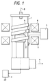
- Fig. 1 shows an embodiment of the plasma CVD apparatus used in the present invention.
- a quartz reactor 1 arranged as capable of reducing the pressure therein, encloses a substrate holder 2, arranged as capable of heating and cooling the substrate and applying the substrate bias voltage to the substrate, and a substrate 3.
- An inductive coupling coil 4 is disposed outside the reactor, and is connected to an unrepresented high-frequency power supply via a matching circuit 5.
- a magnetic field applying means 6 is disposed outside the inductive coupling coil 4 in order to apply a magnetic field in the direction perpendicular to the substrate surface.
- reference numeral 7 is a power supply for the substrate bias voltage.
- Reference numeral 8 designates a gas supply port, to which a valve, a gas cylinder, and a gas-flow-rate regulator, not shown, are connected.
- Reference numeral 9 denotes a vacuum exhaust port, to which a valve, a turbo-molecular pump, and a rotary pump, not shown, are connected.
- Fig. 1 shows a 3-winding inductive coupling coil, but it is noted that the shape of coil, the number of windings, the layout, etc. in the present invention are not limited to those shown in Fig. 1.
- the number of windings can be from 1 to 10 windings, and a plurality of coils can be further arranged in a line to enlarge the plasma-forming region, whereby diamond crystals can be formed on a long-size substrate.
- a diamond crystal was formed, using the CVD apparatus as shown in Fig. 1, in this example.
- Plasma was generated at various frequencies to measure plasma densities, using the starting gas composed of hydrogen: 200 ml/min, methane: 2 ml/min, and oxygen: 0.5 ml/min, the pressure of 50 Pa, and the high-frequency power of 500 W. Results thus obtained are shown in Fig. 2.
- the frequency is less than 40 MHz
- the plasma density is less than 1 ⁇ 1011/cm3.
- the plasma density increases above the frequency of 40 MHz as a border.
- the plasma density becomes about 1012/cm3 at about 80 MHz, and tends to be saturated when the frequency exceeds 80 MHz.
- transmission losses of high-frequency power increase.
- the frequency exceeds 250 MHz, generation of plasma becomes unstable and it becomes impossible to carry out continuous operation over 30 minutes.
- diamond was formed while the frequency of high-frequency wave was fixed at 100 MHz.
- a monocrystalline silicon substrate (diameter: 4 inches, thickness: 400 ⁇ m) was used as the substrate 3 and was heated to 750 °C with a heater. The other conditions were the same as those in the measurement of the plasma density. Further, the substrate was kept at the earth potential and no magnetic field was applied to the substrate. Formation of diamond was continued for 10 hours to obtain a polycrystalline diamond film in the film thickness of about 2.5 ⁇ m. Here, variations of the film thickness was within ⁇ 10 %, which was acceptable.
- Diamond crystals were synthesized at various frequencies, using the CVD apparatus as shown in Fig. 1.
- the forming conditions were as follows: the starting gas was composed of hydrogen: 400 ml/min, methane: 4 ml/min, and oxygen: 1 ml/min; the pressure was 500 Pa; and the high-frequency power was 720 W.
- a monocrystalline silicon substrate (diameter: 4 inches, thickness: 400 ⁇ m) was used as the substrate 3 and the substrate 3 was heated with a heater. Further, the substrate bias voltage was set to the potential of 25 V and the magnetic field was set to 180 gausses near the substrate. The formation period was 8 hours. Film thicknesses and discharge stabilities of diamond films formed are listed in Table 1.
- Discharge Frequency Film Thickness Discharge Stability Sample 1 42 MHz 2 ⁇ m AA Sample 2 100 MHz 4 ⁇ m AA Sample 3 200 MHz 4 ⁇ m A Sample 4 250 MHz 3 ⁇ m B Sample 5 27 MHz not more than 1 ⁇ m AA Sample 6 280 MHz no film formed C AA: Very stable discharge A: Stable discharge B: Practically usable discharge C: Unstable discharge
- the film thickness tends to increase as the strength of magnetic field increases over 150 gausses. This is conceivably because the application of magnetic field increased the plasma density.
- This example observed a dependence on application of the bias voltage to the substrate, of formation of diamond film by the plasma CVD method employing the inductive coupling discharge.
- the forming conditions were the same as those in Example 1 except that the substrate bias voltage was applied to the substrate.
- Table 3 shows the results.
- crystallinities of diamond layers obtained were evaluated by the Raman spectral analysis. According to the Raman spectral analysis, a peak of diamond crystals appeared around 1333 cm ⁇ 1 as a sharp peak, and amorphous carbon or graphite carbon showed broad peaks around 1350 cm ⁇ 1 and 1580 cm ⁇ 1.
- the crystallinity was evaluated by existence of the peak of diamond crystal (1333 cm ⁇ 1) and the peak of amorphous carbon or graphite carbon (1580 cm ⁇ 1), and the ratio thereof (1333 cm ⁇ 1/1580 cm ⁇ 1).
- the crystallinity was evaluated as very good (AA).
- the crystallinity was evaluated as good (A).
- the ratio was less than 1 and the peak of diamond crystal was able to be recognized, a sample was regarded as showing crystallinity (B). Further, when no peak of diamond crystal was confirmed, a sample was regarded as showing no crystallinity (C).
- This example observed effects of combination of application of the bias voltage to the substrate with application of the magnetic field to the vicinity of the substrate.
- Diamond crystals were formed in the same manner as in Example 1 except that the substrate bias voltage was set to 40 V and that the magnetic field was set to 200 gausses near the substrate.
- the film thickness was 7.2 ⁇ m, and according to the Raman spectral analysis, the ratio of peaks of diamond crystals and amorphous carbon or graphite carbon (1333 cm ⁇ 1/1580 cm ⁇ 1) was 2 or more, thus showing very good crystallinity.
- This example confirmed improvements in the diamond forming rate and the crystallinity by the combination of application of the substrate bias voltage with application of the magnetic field to the vicinity of the substrate.
- a semiconductor diamond film was formed in this example, using the apparatus as shown in Fig. 1 and further using application of the substrate bias voltage and application of the magnetic field.
- the substrate was a silicon substrate (3 inches, thickness: 500 ⁇ m) and the starting gas was composed of H2 gas: 100 ml/min, CO (carbon monoxide) gas: 4 ml/min, and B2H2 (diborane, 100 ppm hydrogen-diluted) gas: 2 ml/min.
- the pressure was 150 Pa
- the magnetic field was 200 gausses in the vicinity of the substrate, and the substrate bias voltage was 28 V.
- the frequency of the high-frequency wave was 100 MHz and the high-frequency power was 500 W.
- the substrate temperature was kept at 820 °C and the period of synthesis was 10 hours.
- a diamond thin film was formed in the thickness of about 5.2 ⁇ m on the substrate.
- the diamond film had the electrical resistivity of about 10 ⁇ cm, which showed p-type semiconductor properties.
- a plurality of inductive coupling coils (three coils in the figure) were used, as shown in Fig. 3, to form a coating on a long-size sample.
- a substrate holder 32 arranged as capable of applying the substrate bias voltage, and a substrate 33 are disposed in a quartz reactor 31 arranged as capable of reducing the pressure therein.
- Inductive coupling coils 34, 35 and 36 are disposed outside the reactor, and are connected to a high-frequency power supply, not shown, via matching circuits 37, 38 and 39, respectively.
- a magnetic field applying means 40 is disposed outside the inductive coupling coils in order to apply a magnetic field in the direction perpendicular to the substrate surface.
- Reference numeral 41 represents a power supply for the substrate bias voltage.
- Reference numeral 42 denotes a gas supply port, to which a valve, a gas cylinder, and a gas-flow-rate regulator, not shown, are connected.
- Reference numeral 43 designates a vacuum exhaust port, to which a valve, a turbo molecular pump, and a rotary pump, not shown, are connected.
- the substrate was a pipe (diameter: 2 cm, length: 40 cm) made of molybdenum and the starting gas was composed of H2 gas: 200 ml/min and CO (carbon monoxide) gas: 10 ml/min.
- the pressure was 400 Pa
- the magnetic field was 220 gausses in the vicinity of the substrate
- the substrate bias voltage was 32 V.
- the frequency of the high-frequency wave was 120 MHz and the voltage of 650 W was supplied to each inductive coupling coil.
- the substrate was heated at 800 °C by plasma formed.
- a diamond thin film was formed in the thickness of about 5 ⁇ m on the substrate for the synthesis period of 8 hours.
- variations of film thicknesses of the diamond film formed on the substrate were within ⁇ 10 %, which was very good.
- Diamond crystal thin films can be formed at high forming rates and in large areas by the present invention. Such a method for forming diamond crystals is excellently applicable to methods for forming electronic materials, cutting tools, and wear-resisting members, and the industrial value thereof is high.
- a method for forming a diamond film by a high-frequency plasma CVD method an inductive coupling discharge is used and the frequency of a high-frequency wave is set in the range of from 40 to 250 MHz, whereby a starting gas containing carbon is decomposed in a plasma state and a diamond film is formed on a substrate.
Landscapes
- Chemical & Material Sciences (AREA)
- Engineering & Computer Science (AREA)
- Mechanical Engineering (AREA)
- Chemical Kinetics & Catalysis (AREA)
- General Chemical & Material Sciences (AREA)
- Materials Engineering (AREA)
- Metallurgy (AREA)
- Organic Chemistry (AREA)
- Inorganic Chemistry (AREA)
- Physics & Mathematics (AREA)
- Plasma & Fusion (AREA)
- Crystals, And After-Treatments Of Crystals (AREA)
- Chemical Vapour Deposition (AREA)
Applications Claiming Priority (2)
| Application Number | Priority Date | Filing Date | Title |
|---|---|---|---|
| JP6165182A JPH0827576A (ja) | 1994-07-18 | 1994-07-18 | ダイヤモンド膜の形成方法 |
| JP165182/94 | 1994-07-18 |
Publications (2)
| Publication Number | Publication Date |
|---|---|
| EP0693575A1 true EP0693575A1 (de) | 1996-01-24 |
| EP0693575B1 EP0693575B1 (de) | 1999-05-12 |
Family
ID=15807409
Family Applications (1)
| Application Number | Title | Priority Date | Filing Date |
|---|---|---|---|
| EP95111189A Expired - Lifetime EP0693575B1 (de) | 1994-07-18 | 1995-07-17 | Verfahren zur Herstellung einer Diamantschicht |
Country Status (6)
| Country | Link |
|---|---|
| US (1) | US5720808A (de) |
| EP (1) | EP0693575B1 (de) |
| JP (1) | JPH0827576A (de) |
| KR (1) | KR0184649B1 (de) |
| CN (1) | CN1058534C (de) |
| DE (1) | DE69509594T2 (de) |
Families Citing this family (15)
| Publication number | Priority date | Publication date | Assignee | Title |
|---|---|---|---|---|
| KR100253115B1 (ko) * | 1997-03-05 | 2000-05-01 | 윤덕용 | N-형 반도체 다이아몬드의 제조방법 |
| US6077572A (en) * | 1997-06-18 | 2000-06-20 | Northeastern University | Method of coating edges with diamond-like carbon |
| US6344149B1 (en) | 1998-11-10 | 2002-02-05 | Kennametal Pc Inc. | Polycrystalline diamond member and method of making the same |
| US6423384B1 (en) * | 1999-06-25 | 2002-07-23 | Applied Materials, Inc. | HDP-CVD deposition of low dielectric constant amorphous carbon film |
| US6573030B1 (en) | 2000-02-17 | 2003-06-03 | Applied Materials, Inc. | Method for depositing an amorphous carbon layer |
| US6541397B1 (en) * | 2002-03-29 | 2003-04-01 | Applied Materials, Inc. | Removable amorphous carbon CMP stop |
| CN1969058B (zh) * | 2004-04-19 | 2010-04-14 | 独立行政法人产业技术总合研究所 | 碳膜 |
| JP2008019477A (ja) * | 2006-07-13 | 2008-01-31 | Canon Inc | 真空蒸着装置 |
| CN101200802B (zh) * | 2006-12-13 | 2010-05-12 | 上海坤孚企业(集团)有限公司 | 发动机内壁陶瓷化处理方法 |
| US20080254233A1 (en) * | 2007-04-10 | 2008-10-16 | Kwangduk Douglas Lee | Plasma-induced charge damage control for plasma enhanced chemical vapor deposition processes |
| US20120276743A1 (en) * | 2011-04-26 | 2012-11-01 | Jai-Hyung Won | Methods of forming a carbon type hard mask layer using induced coupled plasma and methods of forming patterns using the same |
| KR101320620B1 (ko) * | 2012-04-10 | 2013-10-23 | 한국과학기술연구원 | 다이아몬드 합성을 위한 화학기상증착 장치 및 이를 이용한 다이아몬드 합성 방법 |
| JP5842761B2 (ja) * | 2012-08-07 | 2016-01-13 | 信越化学工業株式会社 | ダイヤモンドの製造方法及び直流プラズマcvd装置 |
| CN105839071B (zh) * | 2016-04-19 | 2018-01-02 | 中国科学院大学 | 双频电感耦合射频等离子体喷射沉积金刚石的方法 |
| CN107164740B (zh) * | 2017-05-12 | 2019-05-07 | 中国工程物理研究院应用电子学研究所 | 一种采用微波等离子体化学气相沉积法制备金刚石膜的方法 |
Citations (3)
| Publication number | Priority date | Publication date | Assignee | Title |
|---|---|---|---|---|
| JPH0532489A (ja) * | 1991-07-30 | 1993-02-09 | Natl Inst For Res In Inorg Mater | プラズマを用いるダイヤモンドの合成法 |
| EP0539050A1 (de) * | 1991-10-25 | 1993-04-28 | General Electric Company | Chemische Gasphasenabscheidung von Diamanten |
| US5380516A (en) * | 1988-05-28 | 1995-01-10 | Sumitomo Electric Industries, Ltd. | Process for synthesizing diamond in a vapor phase |
Family Cites Families (6)
| Publication number | Priority date | Publication date | Assignee | Title |
|---|---|---|---|---|
| JPH0678851B2 (ja) * | 1988-04-01 | 1994-10-05 | 三洋電機株式会社 | 冷凍装置 |
| US4898748A (en) * | 1988-08-31 | 1990-02-06 | The Board Of Trustees Of Leland Stanford Junior University | Method for enhancing chemical reactivity in thermal plasma processes |
| US5087434A (en) * | 1989-04-21 | 1992-02-11 | The Pennsylvania Research Corporation | Synthesis of diamond powders in the gas phase |
| GB2240113A (en) * | 1990-01-02 | 1991-07-24 | Shell Int Research | Preparation of adsorbent carbonaceous layers |
| US5349154A (en) * | 1991-10-16 | 1994-09-20 | Rockwell International Corporation | Diamond growth by microwave generated plasma flame |
| CA2122995A1 (en) * | 1991-11-05 | 1993-05-13 | Ronald A. Rudder | Chemical vapor deposition of diamond films using water-based plasma discharges |
-
1994
- 1994-07-18 JP JP6165182A patent/JPH0827576A/ja active Pending
-
1995
- 1995-07-14 US US08/502,703 patent/US5720808A/en not_active Expired - Fee Related
- 1995-07-15 KR KR1019950020927A patent/KR0184649B1/ko not_active IP Right Cessation
- 1995-07-17 DE DE69509594T patent/DE69509594T2/de not_active Expired - Fee Related
- 1995-07-17 EP EP95111189A patent/EP0693575B1/de not_active Expired - Lifetime
- 1995-07-18 CN CN95108952A patent/CN1058534C/zh not_active Expired - Fee Related
Patent Citations (3)
| Publication number | Priority date | Publication date | Assignee | Title |
|---|---|---|---|---|
| US5380516A (en) * | 1988-05-28 | 1995-01-10 | Sumitomo Electric Industries, Ltd. | Process for synthesizing diamond in a vapor phase |
| JPH0532489A (ja) * | 1991-07-30 | 1993-02-09 | Natl Inst For Res In Inorg Mater | プラズマを用いるダイヤモンドの合成法 |
| EP0539050A1 (de) * | 1991-10-25 | 1993-04-28 | General Electric Company | Chemische Gasphasenabscheidung von Diamanten |
Non-Patent Citations (3)
| Title |
|---|
| D.E. MEYER ET AL: "R.F. PLASMA CVD OF DIAMOND FROM H2/CH4, H2/CO AND H2/CH4/CO SOURCE GASES", EXTENDED ABSTRACTS, SPRING MEETING, LOS ANGELES, CA,, vol. 89/1, 7 May 1989 (1989-05-07), pages 168, XP000133696 * |
| PATENT ABSTRACTS OF JAPAN vol. 017, no. 321 (C - 1072) 18 June 1993 (1993-06-18) * |
| SUZUKI J ET AL: "The synthesis of diamond films at lower pressure and lower temperature using magneto-microwave plasma CVD", JAPANESE JOURNAL OF APPLIED PHYSICS, PART 2 (LETTERS), FEB. 1989, JAPAN, vol. 28, no. 2, ISSN 0021-4922, pages L281 - L283, XP000069464, DOI: doi:10.1143/JJAP.28.L281 * |
Also Published As
| Publication number | Publication date |
|---|---|
| JPH0827576A (ja) | 1996-01-30 |
| EP0693575B1 (de) | 1999-05-12 |
| KR0184649B1 (ko) | 1999-04-15 |
| US5720808A (en) | 1998-02-24 |
| DE69509594D1 (de) | 1999-06-17 |
| DE69509594T2 (de) | 2000-01-20 |
| CN1121963A (zh) | 1996-05-08 |
| CN1058534C (zh) | 2000-11-15 |
Similar Documents
| Publication | Publication Date | Title |
|---|---|---|
| EP0617147B1 (de) | Herstellungsverfahren für einen Diamant-Kristall | |
| EP0693575B1 (de) | Verfahren zur Herstellung einer Diamantschicht | |
| US4973494A (en) | Microwave enhanced CVD method for depositing a boron nitride and carbon | |
| KR910006784B1 (ko) | 다이어몬드 증착장치와 방법 | |
| EP2108714B1 (de) | Mikrowellen-plasma-cvd-system | |
| EP0442304B1 (de) | Polykristallines CVD-Diamantsubstrat für epitaktisches Aufwachsen von Einkristallhalbleitern | |
| EP0755460B1 (de) | Verfahren zum herstellen von diamantfilmen | |
| JP3428984B2 (ja) | 安定化層及びその製法 | |
| KR970004837B1 (ko) | 반도체기초재료의 제조방법 | |
| JP3509856B2 (ja) | 安定化層のための保護層及びその製法 | |
| JPH0477710B2 (de) | ||
| US5270029A (en) | Carbon substance and its manufacturing method | |
| US5353737A (en) | Method for forming boron-doped semiconducting diamond films | |
| US4599971A (en) | Vapor deposition film forming apparatus | |
| Chattopadhyay et al. | Diamond synthesis by capacitively coupled radio frequency plasma with the addition of direct current power | |
| JPH0226894A (ja) | ダイヤモンドの気相合成方法および装置 | |
| JPH0925197A (ja) | ダイヤモンド膜の形成方法及びその装置 | |
| JPH07133194A (ja) | カーボン膜の形成方法 | |
| Matsumoto et al. | Diamond synthesis by using very high frequency plasmas in parallel plate electrodes configuration | |
| JP3039880B2 (ja) | 炭素膜形成方法 | |
| JPS63265890A (ja) | ダイヤモンド薄膜又はダイヤモンド状薄膜の製造方法 | |
| JPH04175295A (ja) | 半導体ダイヤモンドの製造方法 | |
| Asakura et al. | Diamond synthesis in capacitively coupled 13.56 MHz radio frequency plasma using parallel plate electrodes with the addition of direct current power | |
| Asakura et al. | DIAMOND SYNTHESIS BY VHF PLASMA CVD IN PARALLEL, PLATE ELECTRO DES CONFIGURATION | |
| JPS61236113A (ja) | ダイヤモンド薄膜及びp型ダイヤモンド半導体の製造方法 |
Legal Events
| Date | Code | Title | Description |
|---|---|---|---|
| PUAI | Public reference made under article 153(3) epc to a published international application that has entered the european phase |
Free format text: ORIGINAL CODE: 0009012 |
|
| AK | Designated contracting states |
Kind code of ref document: A1 Designated state(s): DE FR GB IT NL |
|
| 17P | Request for examination filed |
Effective date: 19960610 |
|
| 17Q | First examination report despatched |
Effective date: 19970515 |
|
| GRAG | Despatch of communication of intention to grant |
Free format text: ORIGINAL CODE: EPIDOS AGRA |
|
| GRAG | Despatch of communication of intention to grant |
Free format text: ORIGINAL CODE: EPIDOS AGRA |
|
| GRAH | Despatch of communication of intention to grant a patent |
Free format text: ORIGINAL CODE: EPIDOS IGRA |
|
| GRAH | Despatch of communication of intention to grant a patent |
Free format text: ORIGINAL CODE: EPIDOS IGRA |
|
| GRAA | (expected) grant |
Free format text: ORIGINAL CODE: 0009210 |
|
| AK | Designated contracting states |
Kind code of ref document: B1 Designated state(s): DE FR GB IT NL |
|
| REF | Corresponds to: |
Ref document number: 69509594 Country of ref document: DE Date of ref document: 19990617 |
|
| ET | Fr: translation filed | ||
| PLBE | No opposition filed within time limit |
Free format text: ORIGINAL CODE: 0009261 |
|
| STAA | Information on the status of an ep patent application or granted ep patent |
Free format text: STATUS: NO OPPOSITION FILED WITHIN TIME LIMIT |
|
| 26N | No opposition filed | ||
| REG | Reference to a national code |
Ref country code: GB Ref legal event code: IF02 |
|
| PGFP | Annual fee paid to national office [announced via postgrant information from national office to epo] |
Ref country code: NL Payment date: 20050703 Year of fee payment: 11 |
|
| PGFP | Annual fee paid to national office [announced via postgrant information from national office to epo] |
Ref country code: FR Payment date: 20050708 Year of fee payment: 11 |
|
| PGFP | Annual fee paid to national office [announced via postgrant information from national office to epo] |
Ref country code: GB Payment date: 20050713 Year of fee payment: 11 |
|
| PGFP | Annual fee paid to national office [announced via postgrant information from national office to epo] |
Ref country code: DE Payment date: 20050714 Year of fee payment: 11 |
|
| PG25 | Lapsed in a contracting state [announced via postgrant information from national office to epo] |
Ref country code: GB Free format text: LAPSE BECAUSE OF NON-PAYMENT OF DUE FEES Effective date: 20060717 |
|
| PGFP | Annual fee paid to national office [announced via postgrant information from national office to epo] |
Ref country code: IT Payment date: 20060731 Year of fee payment: 12 |
|
| PG25 | Lapsed in a contracting state [announced via postgrant information from national office to epo] |
Ref country code: NL Free format text: LAPSE BECAUSE OF NON-PAYMENT OF DUE FEES Effective date: 20070201 Ref country code: DE Free format text: LAPSE BECAUSE OF NON-PAYMENT OF DUE FEES Effective date: 20070201 |
|
| GBPC | Gb: european patent ceased through non-payment of renewal fee |
Effective date: 20060717 |
|
| NLV4 | Nl: lapsed or anulled due to non-payment of the annual fee |
Effective date: 20070201 |
|
| REG | Reference to a national code |
Ref country code: FR Ref legal event code: ST Effective date: 20070330 |
|
| PG25 | Lapsed in a contracting state [announced via postgrant information from national office to epo] |
Ref country code: FR Free format text: LAPSE BECAUSE OF NON-PAYMENT OF DUE FEES Effective date: 20060731 |
|
| PG25 | Lapsed in a contracting state [announced via postgrant information from national office to epo] |
Ref country code: IT Free format text: LAPSE BECAUSE OF NON-PAYMENT OF DUE FEES Effective date: 20070717 |