EP0688053A1 - Module semi-conducteur de puissance à basse inductance - Google Patents
Module semi-conducteur de puissance à basse inductance Download PDFInfo
- Publication number
- EP0688053A1 EP0688053A1 EP95201442A EP95201442A EP0688053A1 EP 0688053 A1 EP0688053 A1 EP 0688053A1 EP 95201442 A EP95201442 A EP 95201442A EP 95201442 A EP95201442 A EP 95201442A EP 0688053 A1 EP0688053 A1 EP 0688053A1
- Authority
- EP
- European Patent Office
- Prior art keywords
- power semiconductor
- connections
- heat sink
- module
- semiconductor module
- Prior art date
- Legal status (The legal status is an assumption and is not a legal conclusion. Google has not performed a legal analysis and makes no representation as to the accuracy of the status listed.)
- Granted
Links
Images
Classifications
-
- H—ELECTRICITY
- H01—ELECTRIC ELEMENTS
- H01L—SEMICONDUCTOR DEVICES NOT COVERED BY CLASS H10
- H01L25/00—Assemblies consisting of a plurality of individual semiconductor or other solid state devices ; Multistep manufacturing processes thereof
- H01L25/18—Assemblies consisting of a plurality of individual semiconductor or other solid state devices ; Multistep manufacturing processes thereof the devices being of types provided for in two or more different subgroups of the same main group of groups H01L27/00 - H01L33/00, or in a single subclass of H10K, H10N
-
- H—ELECTRICITY
- H01—ELECTRIC ELEMENTS
- H01L—SEMICONDUCTOR DEVICES NOT COVERED BY CLASS H10
- H01L23/00—Details of semiconductor or other solid state devices
- H01L23/34—Arrangements for cooling, heating, ventilating or temperature compensation ; Temperature sensing arrangements
- H01L23/46—Arrangements for cooling, heating, ventilating or temperature compensation ; Temperature sensing arrangements involving the transfer of heat by flowing fluids
- H01L23/473—Arrangements for cooling, heating, ventilating or temperature compensation ; Temperature sensing arrangements involving the transfer of heat by flowing fluids by flowing liquids
-
- H—ELECTRICITY
- H01—ELECTRIC ELEMENTS
- H01L—SEMICONDUCTOR DEVICES NOT COVERED BY CLASS H10
- H01L25/00—Assemblies consisting of a plurality of individual semiconductor or other solid state devices ; Multistep manufacturing processes thereof
- H01L25/03—Assemblies consisting of a plurality of individual semiconductor or other solid state devices ; Multistep manufacturing processes thereof all the devices being of a type provided for in the same subgroup of groups H01L27/00 - H01L33/00, or in a single subclass of H10K, H10N, e.g. assemblies of rectifier diodes
- H01L25/04—Assemblies consisting of a plurality of individual semiconductor or other solid state devices ; Multistep manufacturing processes thereof all the devices being of a type provided for in the same subgroup of groups H01L27/00 - H01L33/00, or in a single subclass of H10K, H10N, e.g. assemblies of rectifier diodes the devices not having separate containers
- H01L25/065—Assemblies consisting of a plurality of individual semiconductor or other solid state devices ; Multistep manufacturing processes thereof all the devices being of a type provided for in the same subgroup of groups H01L27/00 - H01L33/00, or in a single subclass of H10K, H10N, e.g. assemblies of rectifier diodes the devices not having separate containers the devices being of a type provided for in group H01L27/00
- H01L25/0652—Assemblies consisting of a plurality of individual semiconductor or other solid state devices ; Multistep manufacturing processes thereof all the devices being of a type provided for in the same subgroup of groups H01L27/00 - H01L33/00, or in a single subclass of H10K, H10N, e.g. assemblies of rectifier diodes the devices not having separate containers the devices being of a type provided for in group H01L27/00 the devices being arranged next and on each other, i.e. mixed assemblies
-
- H—ELECTRICITY
- H01—ELECTRIC ELEMENTS
- H01L—SEMICONDUCTOR DEVICES NOT COVERED BY CLASS H10
- H01L25/00—Assemblies consisting of a plurality of individual semiconductor or other solid state devices ; Multistep manufacturing processes thereof
- H01L25/03—Assemblies consisting of a plurality of individual semiconductor or other solid state devices ; Multistep manufacturing processes thereof all the devices being of a type provided for in the same subgroup of groups H01L27/00 - H01L33/00, or in a single subclass of H10K, H10N, e.g. assemblies of rectifier diodes
- H01L25/04—Assemblies consisting of a plurality of individual semiconductor or other solid state devices ; Multistep manufacturing processes thereof all the devices being of a type provided for in the same subgroup of groups H01L27/00 - H01L33/00, or in a single subclass of H10K, H10N, e.g. assemblies of rectifier diodes the devices not having separate containers
- H01L25/07—Assemblies consisting of a plurality of individual semiconductor or other solid state devices ; Multistep manufacturing processes thereof all the devices being of a type provided for in the same subgroup of groups H01L27/00 - H01L33/00, or in a single subclass of H10K, H10N, e.g. assemblies of rectifier diodes the devices not having separate containers the devices being of a type provided for in group H01L29/00
- H01L25/071—Assemblies consisting of a plurality of individual semiconductor or other solid state devices ; Multistep manufacturing processes thereof all the devices being of a type provided for in the same subgroup of groups H01L27/00 - H01L33/00, or in a single subclass of H10K, H10N, e.g. assemblies of rectifier diodes the devices not having separate containers the devices being of a type provided for in group H01L29/00 the devices being arranged next and on each other, i.e. mixed assemblies
-
- H—ELECTRICITY
- H02—GENERATION; CONVERSION OR DISTRIBUTION OF ELECTRIC POWER
- H02M—APPARATUS FOR CONVERSION BETWEEN AC AND AC, BETWEEN AC AND DC, OR BETWEEN DC AND DC, AND FOR USE WITH MAINS OR SIMILAR POWER SUPPLY SYSTEMS; CONVERSION OF DC OR AC INPUT POWER INTO SURGE OUTPUT POWER; CONTROL OR REGULATION THEREOF
- H02M7/00—Conversion of ac power input into dc power output; Conversion of dc power input into ac power output
- H02M7/003—Constructional details, e.g. physical layout, assembly, wiring or busbar connections
-
- H—ELECTRICITY
- H05—ELECTRIC TECHNIQUES NOT OTHERWISE PROVIDED FOR
- H05K—PRINTED CIRCUITS; CASINGS OR CONSTRUCTIONAL DETAILS OF ELECTRIC APPARATUS; MANUFACTURE OF ASSEMBLAGES OF ELECTRICAL COMPONENTS
- H05K7/00—Constructional details common to different types of electric apparatus
- H05K7/14—Mounting supporting structure in casing or on frame or rack
- H05K7/1422—Printed circuit boards receptacles, e.g. stacked structures, electronic circuit modules or box like frames
- H05K7/1427—Housings
- H05K7/1432—Housings specially adapted for power drive units or power converters
- H05K7/14329—Housings specially adapted for power drive units or power converters specially adapted for the configuration of power bus bars
-
- H—ELECTRICITY
- H05—ELECTRIC TECHNIQUES NOT OTHERWISE PROVIDED FOR
- H05K—PRINTED CIRCUITS; CASINGS OR CONSTRUCTIONAL DETAILS OF ELECTRIC APPARATUS; MANUFACTURE OF ASSEMBLAGES OF ELECTRICAL COMPONENTS
- H05K7/00—Constructional details common to different types of electric apparatus
- H05K7/20—Modifications to facilitate cooling, ventilating, or heating
- H05K7/2089—Modifications to facilitate cooling, ventilating, or heating for power electronics, e.g. for inverters for controlling motor
- H05K7/20927—Liquid coolant without phase change
-
- H—ELECTRICITY
- H01—ELECTRIC ELEMENTS
- H01L—SEMICONDUCTOR DEVICES NOT COVERED BY CLASS H10
- H01L2924/00—Indexing scheme for arrangements or methods for connecting or disconnecting semiconductor or solid-state bodies as covered by H01L24/00
- H01L2924/0001—Technical content checked by a classifier
- H01L2924/0002—Not covered by any one of groups H01L24/00, H01L24/00 and H01L2224/00
-
- H—ELECTRICITY
- H01—ELECTRIC ELEMENTS
- H01L—SEMICONDUCTOR DEVICES NOT COVERED BY CLASS H10
- H01L2924/00—Indexing scheme for arrangements or methods for connecting or disconnecting semiconductor or solid-state bodies as covered by H01L24/00
- H01L2924/30—Technical effects
- H01L2924/301—Electrical effects
- H01L2924/3011—Impedance
Definitions
- the invention relates to the field of power semiconductor electronics.
- a power semiconductor module generally comprises several semiconductor components that can be combined to form a logical functional unit. Examples are Rectifier, single switch with anti-parallel diode or phase modules. Modules differ from the disk cells common today in the high-performance semiconductor sector in that the cooling and power connections are electrically insulated from one another.
- Modules are widely used today in the power range up to 1200 V and some 100 A and are mainly used in industrial drives.
- Modules for high currents generally consist of a number of individual components that are connected in parallel in the module, or several modules are connected in parallel.
- the essence of the invention is therefore that power semiconductor modules are provided on both sides of a heat sink and that these are contacted by a low-inductance contact plate package.
- a preferred exemplary embodiment is characterized in that the power semiconductor modules form one half of a half-bridge module on each side of the heat sink.
- the power semiconductor modules preferably comprise a substrate to which at least one power semiconductor switch with an anti-parallel diode is applied.
- a cooling liquid advantageously flows through the heat sink and the entire arrangement is integrated into a protective housing.
- the advantage of the construction according to the invention is, in particular, that the module has sufficient cooling, since assemblies are attached to both sides of the heat sink and the assemblies are mounted directly on the heat sink. This eliminates the heat transfer from the module to the cooler compared to known modules.
- inverter circuits for generating AC voltage from a DC voltage.
- two switches and associated diodes are required for each phase.
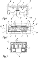
- This so-called half-bridge represents the smallest logic module for an inverter circuit. Such a half-bridge is shown in FIG. 1 .
- a half-bridge can only be assembled from two individual switching modules for maximum performance, since the integration of the entire function into just one module would result in a very large-area module, which is not possible due to the limitations explained above.
- the invention therefore relates to a half-bridge module which is suitable for the highest performance.
- a module is shown in section in FIG .
- It comprises a heat sink (3) which is traversed by cooling channels (7) and has connections (6) for a cooling medium (for example water with an anti-freeze additive).
- Substrates (8) are attached to both sides of the heat sink (3).
- the substrates (8) consist of an electrically insulating but nevertheless highly heat-conductive material, such as aluminum oxide, aluminum nitride or berylium oxide. Depending on the material of the heat sink, these substrates are either soldered on (eg DCB aluminum oxide ceramic on copper) or glued on (eg aluminum nitride ceramic on aluminum). Other connection techniques such as plasma spraying are also conceivable.
- the individual components (for example IGBTs and diodes) are already mounted on the top of the substrate (8), connected to one another and pre-tested.
- a top view of such a loaded substrate (8) is shown in FIG. 3 .
- each substrate comprise the function of a power semiconductor switch (10) with a diode (11) connected in anti-parallel.
- the power semiconductor switch (10) and the diode (11) can in turn be composed of several discrete components.
- an assembled substrate (8) forms a power semiconductor module (2) with basically any function.
- These power semiconductor modules (2) are now contacted by means of suitably shaped, electrically conductive contact plates (4).
- the sheets (4) preferably consist of the same material or a material which is adapted to the heat sink (3) with regard to the coefficient of thermal expansion. Insulating plates (not shown) are inserted between the individual sheets (4). The contact plates (4) and the insulating plates are connected to a stack (e.g. glued) and mechanically connected to the heat sink (3).
- These laminated cores are now used on both sides of the heat sink (3) for the low-inductance connection of the individual substrates (8).
- the substrates are connected to the respective laminated core using bonded or soldered connections (depending on the material of the metal sheets).
- each side comprised of the heat sink (3) represented the single switch unit mentioned. Accordingly, each side comprised of the heat sink (3) a "quarter bridge" and the entire module (1) was a half bridge. As can be seen in FIG. 1, such a half bridge has a positive connection (12), a negative connection (13) and an AC voltage connection (14) .
- the switches (10) are switched on and off via a control connection (15, 16).
- a measuring connection (17, 18) can also be provided for error monitoring.
- the contact plate package for contacting such a half-bridge module (1) comprises the corresponding number of contact plates (4).
- the contact plates (4) for the main connections are preferably arranged as shown in FIG.
- the DC voltage connections (12 and 13) are brought in from one side and the AC voltage connection (14) from the other side. At the same time, this forms the connection between the quarter bridges arranged on different sides of the heat sink (3).
- the module (1) thus created is protected against external influences by providing it with a housing (5) and, for example, casting it with a silicone gel.
- the module can be optimally connected by means of screw connections, but preferably plug connections.
- the exemplary embodiment shown is based on a plug connection on the DC side.
- the center bar made of insulating material guides the connector (e.g. wedge-shaped) and at the same time ensures that the necessary creepage distances are observed.
Landscapes
- Engineering & Computer Science (AREA)
- Microelectronics & Electronic Packaging (AREA)
- Power Engineering (AREA)
- Physics & Mathematics (AREA)
- Condensed Matter Physics & Semiconductors (AREA)
- General Physics & Mathematics (AREA)
- Computer Hardware Design (AREA)
- Thermal Sciences (AREA)
- Cooling Or The Like Of Semiconductors Or Solid State Devices (AREA)
Applications Claiming Priority (2)
| Application Number | Priority Date | Filing Date | Title |
|---|---|---|---|
| DE4421319A DE4421319A1 (de) | 1994-06-17 | 1994-06-17 | Niederinduktives Leistungshalbleitermodul |
| DE4421319 | 1994-06-17 |
Publications (2)
| Publication Number | Publication Date |
|---|---|
| EP0688053A1 true EP0688053A1 (fr) | 1995-12-20 |
| EP0688053B1 EP0688053B1 (fr) | 1999-01-13 |
Family
ID=6520891
Family Applications (1)
| Application Number | Title | Priority Date | Filing Date |
|---|---|---|---|
| EP95201442A Expired - Lifetime EP0688053B1 (fr) | 1994-06-17 | 1995-06-01 | Module semi-conducteur de puissance à basse inductance |
Country Status (5)
| Country | Link |
|---|---|
| US (1) | US5574312A (fr) |
| EP (1) | EP0688053B1 (fr) |
| JP (1) | JPH088397A (fr) |
| CN (1) | CN1120737A (fr) |
| DE (2) | DE4421319A1 (fr) |
Cited By (5)
| Publication number | Priority date | Publication date | Assignee | Title |
|---|---|---|---|---|
| EP0822647A1 (fr) * | 1996-08-01 | 1998-02-04 | Hitachi, Ltd. | Appareil électrique pourvu d'ailettes radiantes |
| WO2005051063A1 (fr) * | 2003-11-18 | 2005-06-02 | Toyota Jidosha Kabushiki Kaisha | Structure de refroidissement pour dispositif electrique |
| WO2007118831A2 (fr) * | 2006-04-19 | 2007-10-25 | Osram Gesellschaft mit beschränkter Haftung | Module composant électronique |
| EP3147941A1 (fr) | 2015-09-23 | 2017-03-29 | ABB Technology AG | Produit semi-fini et procédé de fabrication d'un module semi-conducteur de puissance |
| US10283454B2 (en) | 2015-05-22 | 2019-05-07 | Abb Schweiz Ag | Power semiconductor module |
Families Citing this family (54)
| Publication number | Priority date | Publication date | Assignee | Title |
|---|---|---|---|---|
| US5892279A (en) * | 1995-12-11 | 1999-04-06 | Northrop Grumman Corporation | Packaging for electronic power devices and applications using the packaging |
| JP3444081B2 (ja) * | 1996-02-28 | 2003-09-08 | 株式会社日立製作所 | ダイオード及び電力変換装置 |
| US6954368B1 (en) | 1996-07-22 | 2005-10-11 | HYDRO-QUéBEC | Low stray interconnection inductance power converting molecule for converting a DC voltage into an AC voltage, and a method therefor |
| US6060795A (en) * | 1998-03-18 | 2000-05-09 | Intersil Corporation | Semiconductor power pack |
| US6057612A (en) * | 1998-07-02 | 2000-05-02 | Intersil Corporation | Flat power pack |
| RU2190284C2 (ru) | 1998-07-07 | 2002-09-27 | Закрытое акционерное общество "Техно-ТМ" | Двусторонний электронный прибор |
| DE19833491A1 (de) | 1998-07-24 | 2000-02-03 | Siemens Ag | Niederinduktive Verschienung für einen Dreipunkt-Phasenbaustein |
| DE19847029A1 (de) * | 1998-10-13 | 2000-04-27 | Semikron Elektronik Gmbh | Umrichter mit niederinduktivem Kondensator im Zwischenkreis |
| DE19851161A1 (de) * | 1998-11-06 | 2000-05-11 | Abb Daimler Benz Transp | Stromrichtergerät mit Gleich- und Wechselspannungsverschienung |
| JP2000164800A (ja) * | 1998-11-30 | 2000-06-16 | Mitsubishi Electric Corp | 半導体モジュール |
| FR2809281B1 (fr) * | 2000-05-22 | 2002-07-12 | Alstom | Dispositif electronique de puissance |
| DE10037533C1 (de) * | 2000-08-01 | 2002-01-31 | Semikron Elektronik Gmbh | Induktivitätsarme Schaltungsanordnung |
| JP2002223589A (ja) * | 2001-01-25 | 2002-08-09 | Mitsubishi Heavy Ind Ltd | バッテリフォークリフト用モータコントローラ |
| JP4573467B2 (ja) * | 2001-05-25 | 2010-11-04 | 三菱電機株式会社 | パワー半導体装置 |
| US7145254B2 (en) * | 2001-07-26 | 2006-12-05 | Denso Corporation | Transfer-molded power device and method for manufacturing transfer-molded power device |
| DE10294631D2 (de) * | 2001-09-28 | 2004-10-07 | Siemens Ag | Anordnung mit Leistungshalbleiterbauelementen zur Leistungssteuerung hoher Ströme und Anwendung der Anordnung |
| US6885562B2 (en) * | 2001-12-28 | 2005-04-26 | Medtronic Physio-Control Manufacturing Corporation | Circuit package and method for making the same |
| US7505294B2 (en) * | 2003-05-16 | 2009-03-17 | Continental Automotive Systems Us, Inc. | Tri-level inverter |
| FR2855912B1 (fr) * | 2003-06-04 | 2006-04-14 | Alstom | Cellule de commutation de puissance, et procede de fabrication de la cellule |
| JP4491244B2 (ja) * | 2004-01-07 | 2010-06-30 | 三菱電機株式会社 | 電力半導体装置 |
| US7327024B2 (en) * | 2004-11-24 | 2008-02-05 | General Electric Company | Power module, and phase leg assembly |
| JP4106061B2 (ja) * | 2005-04-22 | 2008-06-25 | 三菱電機株式会社 | パワーユニット装置及び電力変換装置 |
| JP2006303290A (ja) * | 2005-04-22 | 2006-11-02 | Mitsubishi Electric Corp | 半導体装置 |
| JP2008027935A (ja) * | 2006-07-18 | 2008-02-07 | Hitachi Ltd | パワー半導体装置 |
| DE102007003875A1 (de) * | 2007-01-25 | 2008-08-07 | Siemens Ag | Stromrichter |
| US7773381B2 (en) * | 2007-09-26 | 2010-08-10 | Rohm Co., Ltd. | Semiconductor device |
| JP5678407B2 (ja) * | 2009-03-02 | 2015-03-04 | 日産自動車株式会社 | 半導体装置 |
| US8742814B2 (en) | 2009-07-15 | 2014-06-03 | Yehuda Binder | Sequentially operated modules |
| KR101022906B1 (ko) * | 2009-07-20 | 2011-03-16 | 삼성전기주식회사 | 전력반도체 모듈 및 그 제조방법 |
| US8602833B2 (en) | 2009-08-06 | 2013-12-10 | May Patents Ltd. | Puzzle with conductive path |
| DE102010002627B4 (de) * | 2010-03-05 | 2023-10-05 | Infineon Technologies Ag | Niederinduktive Leistungshalbleiterbaugruppen |
| JP5174085B2 (ja) * | 2010-05-20 | 2013-04-03 | 三菱電機株式会社 | 半導体装置 |
| US8622754B2 (en) * | 2011-07-31 | 2014-01-07 | General Electric Company | Flexible power connector |
| US9597607B2 (en) | 2011-08-26 | 2017-03-21 | Littlebits Electronics Inc. | Modular electronic building systems with magnetic interconnections and methods of using the same |
| US11330714B2 (en) | 2011-08-26 | 2022-05-10 | Sphero, Inc. | Modular electronic building systems with magnetic interconnections and methods of using the same |
| US9019718B2 (en) | 2011-08-26 | 2015-04-28 | Littlebits Electronics Inc. | Modular electronic building systems with magnetic interconnections and methods of using the same |
| US8637964B2 (en) * | 2011-10-26 | 2014-01-28 | Infineon Technologies Ag | Low stray inductance power module |
| US9099930B2 (en) | 2012-06-22 | 2015-08-04 | General Electric Company | Power converter and method of assembling the same |
| US8942020B2 (en) | 2012-06-22 | 2015-01-27 | General Electric Company | Three-level phase leg for a power converter |
| JP5950800B2 (ja) * | 2012-11-21 | 2016-07-13 | 株式会社日立製作所 | 電力変換装置 |
| JP6124742B2 (ja) * | 2013-09-05 | 2017-05-10 | 三菱電機株式会社 | 半導体装置 |
| JP6541957B2 (ja) * | 2014-10-23 | 2019-07-10 | ローム株式会社 | パワーモジュール |
| DE102015115271B4 (de) | 2015-09-10 | 2021-07-15 | Infineon Technologies Ag | Elektronikbaugruppe mit entstörkondensatoren und verfahren zum betrieb der elektronikbaugruppe |
| DE102016211648A1 (de) * | 2016-06-28 | 2017-12-28 | Zf Friedrichshafen Ag | Elektronikmodul und Modulstapel |
| US10410952B2 (en) | 2016-12-15 | 2019-09-10 | Infineon Technologies Ag | Power semiconductor packages having a substrate with two or more metal layers and one or more polymer-based insulating layers for separating the metal layers |
| US10008411B2 (en) | 2016-12-15 | 2018-06-26 | Infineon Technologies Ag | Parallel plate waveguide for power circuits |
| US10607919B2 (en) | 2017-04-28 | 2020-03-31 | Semiconductor Components Industries, Llc | Semiconductor package having junction cooling pipes embedded in substrates |
| DE102017209515A1 (de) | 2017-06-06 | 2018-12-06 | Bayerische Motoren Werke Aktiengesellschaft | Leistungsumrichtermodul und Verfahren zu dessen Herstellung |
| WO2019012677A1 (fr) | 2017-07-14 | 2019-01-17 | 新電元工業株式会社 | Module électronique |
| CN108880286A (zh) * | 2018-08-16 | 2018-11-23 | 全球能源互联网研究院有限公司 | 基于芯片与系统统一优化的高压直流阀堆结构设计方法 |
| US11616844B2 (en) | 2019-03-14 | 2023-03-28 | Sphero, Inc. | Modular electronic and digital building systems and methods of using the same |
| FR3105716B1 (fr) * | 2019-12-18 | 2022-07-01 | Valeo Siemens Eautomotive France Sas | Équipement électrique comprenant une barre de connexion électrique refroidie par deux faces d’un dissipateur thermique |
| EP3893615B1 (fr) * | 2020-04-07 | 2024-10-02 | Hamilton Sundstrand Corporation | Ensembles convertisseurs de puissance avec barres omnibus |
| DE102022208130A1 (de) | 2022-08-04 | 2024-02-15 | Zf Friedrichshafen Ag | Halbbrückenmodul für einen Stromrichter mit einer kompakten Bauweise und gleich-zeitig effizienter Kühlung von Halbleiterschaltelementen |
Citations (6)
| Publication number | Priority date | Publication date | Assignee | Title |
|---|---|---|---|---|
| JPS60101958A (ja) * | 1983-11-08 | 1985-06-06 | Rohm Co Ltd | ダイオ−ド装置の製造方法 |
| EP0228953A1 (fr) * | 1985-12-17 | 1987-07-15 | Thomson-Csf | Boîtier d'encapsulation d'un circuit électronique |
| US4989070A (en) * | 1988-11-10 | 1991-01-29 | Coriolis Corporation | Modular heat sink structure |
| DE3937045A1 (de) | 1989-11-07 | 1991-05-08 | Abb Ixys Semiconductor Gmbh | Leistungshalbleitermodul |
| DE4103486A1 (de) | 1991-02-06 | 1992-08-20 | Abb Patent Gmbh | Anordnung zur kuehlung waermeerzeugender bauelemente |
| EP0551741A1 (fr) * | 1991-12-13 | 1993-07-21 | Hewlett-Packard Company | Intégration de conduites de chaleur et d'interconnexions électriques pour des modules de puces |
Family Cites Families (11)
| Publication number | Priority date | Publication date | Assignee | Title |
|---|---|---|---|---|
| DE2611749C3 (de) * | 1976-03-19 | 1980-11-13 | Siemens Ag, 1000 Berlin Und 8000 Muenchen | Halbleiteranordnung mit einem über Spannbolzen durch Druck kontaktierbaren Halbleiterbauelement |
| DE3931634A1 (de) * | 1989-09-22 | 1991-04-04 | Telefunken Electronic Gmbh | Halbleiterbauelement |
| JPH03136338A (ja) * | 1989-10-23 | 1991-06-11 | Mitsubishi Electric Corp | 半導体装置およびその製造のためのロウ付け方法 |
| US5077595A (en) * | 1990-01-25 | 1991-12-31 | Mitsubishi Denki Kabushiki Kaisha | Semiconductor device |
| DE9113499U1 (de) * | 1991-09-11 | 1992-04-30 | Export-Contor Außenhandelsgesellschaft mbH, 8500 Nürnberg | Elektronische Schaltung |
| JPH05166969A (ja) * | 1991-10-14 | 1993-07-02 | Fuji Electric Co Ltd | 半導体装置 |
| DE4217289C2 (de) * | 1992-05-25 | 1996-08-29 | Mannesmann Ag | Fluidgekühlte Leistungstransistoranordnung |
| JP2838625B2 (ja) * | 1992-09-08 | 1998-12-16 | 株式会社日立製作所 | 半導体モジュール |
| JPH06233554A (ja) * | 1993-01-28 | 1994-08-19 | Fuji Electric Co Ltd | インバータ装置 |
| US5444295A (en) * | 1993-09-07 | 1995-08-22 | Delco Electronics Corp. | Linear dual switch module |
| US5408128A (en) * | 1993-09-15 | 1995-04-18 | International Rectifier Corporation | High power semiconductor device module with low thermal resistance and simplified manufacturing |
-
1994
- 1994-06-17 DE DE4421319A patent/DE4421319A1/de not_active Withdrawn
-
1995
- 1995-05-05 US US08/435,617 patent/US5574312A/en not_active Expired - Fee Related
- 1995-06-01 DE DE59504782T patent/DE59504782D1/de not_active Expired - Fee Related
- 1995-06-01 EP EP95201442A patent/EP0688053B1/fr not_active Expired - Lifetime
- 1995-06-07 JP JP7140776A patent/JPH088397A/ja active Pending
- 1995-06-16 CN CN95107021A patent/CN1120737A/zh active Pending
Patent Citations (7)
| Publication number | Priority date | Publication date | Assignee | Title |
|---|---|---|---|---|
| JPS60101958A (ja) * | 1983-11-08 | 1985-06-06 | Rohm Co Ltd | ダイオ−ド装置の製造方法 |
| EP0228953A1 (fr) * | 1985-12-17 | 1987-07-15 | Thomson-Csf | Boîtier d'encapsulation d'un circuit électronique |
| US4989070A (en) * | 1988-11-10 | 1991-01-29 | Coriolis Corporation | Modular heat sink structure |
| DE3937045A1 (de) | 1989-11-07 | 1991-05-08 | Abb Ixys Semiconductor Gmbh | Leistungshalbleitermodul |
| EP0427143A2 (fr) * | 1989-11-07 | 1991-05-15 | IXYS Semiconductor GmbH | Module à semi-conducteur de puissance |
| DE4103486A1 (de) | 1991-02-06 | 1992-08-20 | Abb Patent Gmbh | Anordnung zur kuehlung waermeerzeugender bauelemente |
| EP0551741A1 (fr) * | 1991-12-13 | 1993-07-21 | Hewlett-Packard Company | Intégration de conduites de chaleur et d'interconnexions électriques pour des modules de puces |
Non-Patent Citations (2)
| Title |
|---|
| PATENT ABSTRACTS OF JAPAN vol. 9, no. 251 (E - 348)<1974> 8 October 1985 (1985-10-08) * |
| R. NARAYANAN ET AL.: "thermal and mechanical analysis of flip-chips on a liquid-cooled multichip module", 1993 PROC. 43RD ELECTRONIC COMPONENTS & TECHNOLOGY CONFERENCE, June 1993 (1993-06-01), FLORIDA, US, pages 22 - 31, XP000380008 * |
Cited By (9)
| Publication number | Priority date | Publication date | Assignee | Title |
|---|---|---|---|---|
| EP0822647A1 (fr) * | 1996-08-01 | 1998-02-04 | Hitachi, Ltd. | Appareil électrique pourvu d'ailettes radiantes |
| US5940272A (en) * | 1996-08-01 | 1999-08-17 | Hitachi, Ltd. | Electric apparatus having heat radiating fin |
| WO2005051063A1 (fr) * | 2003-11-18 | 2005-06-02 | Toyota Jidosha Kabushiki Kaisha | Structure de refroidissement pour dispositif electrique |
| US7453695B2 (en) | 2003-11-18 | 2008-11-18 | Toyota Jidosha Kabushiki Kaisha | Cooling structure of electric device |
| WO2007118831A2 (fr) * | 2006-04-19 | 2007-10-25 | Osram Gesellschaft mit beschränkter Haftung | Module composant électronique |
| WO2007118831A3 (fr) * | 2006-04-19 | 2008-02-21 | Patent Treuhand Ges Fuer Elektrische Gluehlampen Mbh | Module composant électronique |
| US8164904B2 (en) | 2006-04-19 | 2012-04-24 | Osram Ag | Electronic component module |
| US10283454B2 (en) | 2015-05-22 | 2019-05-07 | Abb Schweiz Ag | Power semiconductor module |
| EP3147941A1 (fr) | 2015-09-23 | 2017-03-29 | ABB Technology AG | Produit semi-fini et procédé de fabrication d'un module semi-conducteur de puissance |
Also Published As
| Publication number | Publication date |
|---|---|
| DE4421319A1 (de) | 1995-12-21 |
| JPH088397A (ja) | 1996-01-12 |
| DE59504782D1 (de) | 1999-02-25 |
| EP0688053B1 (fr) | 1999-01-13 |
| CN1120737A (zh) | 1996-04-17 |
| US5574312A (en) | 1996-11-12 |
Similar Documents
| Publication | Publication Date | Title |
|---|---|---|
| EP0688053B1 (fr) | Module semi-conducteur de puissance à basse inductance | |
| EP0427143B1 (fr) | Module à semi-conducteur de puissance | |
| DE112015002001B4 (de) | Halbleitermodul | |
| EP0841843B1 (fr) | Module de puissance pour la commande de moteurs électriques | |
| DE102012218579B4 (de) | Niederinduktives Kondensatormodul und Leistungssystem mit einem solchen | |
| DE69226141T2 (de) | Dreiphasiger dreistufiger Wechselrichter | |
| DE69216016T2 (de) | Halbleiteranordnung | |
| EP1318547B1 (fr) | Module semi-conducteur à haut prestation | |
| DE19900603A1 (de) | Elektronisches Halbleitermodul | |
| DE102019112935B4 (de) | Halbleitermodul | |
| DE102018100468A1 (de) | Leistungsmodul für wechselrichter-schaltvorrichtungen, die von wirbelströmen abgeschirmte gate-spulen aufweisen | |
| DE112018005978T5 (de) | Halbleitervorrichtung | |
| EP1178595B1 (fr) | Disposition à faible induction pour circuit | |
| EP0597144A1 (fr) | Dispositif électronique de puissance en circuit hybride | |
| DE102020214045A1 (de) | Halbbrücke für einen elektrischen Antrieb eines Elektrofahrzeugs oder eines Hybridfahrzeugs, Leistungsmodul für einen Inverter und Inverter | |
| DE102019112936A1 (de) | Halbleitermodul | |
| DE4133199C2 (de) | Halbleiterbauelement mit isolationsbeschichtetem Metallsubstrat | |
| DE112020006374T5 (de) | Leistungsmodul mit verbesserten elektrischen und thermischen Charakteristiken | |
| DE102019217502B4 (de) | Halbleitervorrichtung, elektrische Leistungsumwandlungseinrichtung und Verfahren zum Herstellen einer Halbleitervorrichtung | |
| DE102019212727B4 (de) | Halbleitervorrichtung und elektrische Leistungsumwandlungseinrichtung | |
| EP0738008A2 (fr) | Module à semi-conducteur de puissance | |
| DE102019112934A1 (de) | Halbleitermodul | |
| EP0710983B1 (fr) | Module à pont | |
| DE3831610A1 (de) | Schaltnetzteil | |
| DE102020204358A1 (de) | Halbbrückenmodul für einen Inverter eines elektrischen Antriebs eines Elektrofahrzeugs oder eines Hybridfahrzeugs und Inverter für einen elektrischen Antrieb eines Elektrofahrzeugs oder eines Hybridfahrzeugs |
Legal Events
| Date | Code | Title | Description |
|---|---|---|---|
| PUAI | Public reference made under article 153(3) epc to a published international application that has entered the european phase |
Free format text: ORIGINAL CODE: 0009012 |
|
| AK | Designated contracting states |
Kind code of ref document: A1 Designated state(s): CH DE FR GB LI |
|
| 17P | Request for examination filed |
Effective date: 19960509 |
|
| RAP1 | Party data changed (applicant data changed or rights of an application transferred) |
Owner name: ASEA BROWN BOVERI AG |
|
| 17Q | First examination report despatched |
Effective date: 19970731 |
|
| GRAG | Despatch of communication of intention to grant |
Free format text: ORIGINAL CODE: EPIDOS AGRA |
|
| GRAG | Despatch of communication of intention to grant |
Free format text: ORIGINAL CODE: EPIDOS AGRA |
|
| GRAG | Despatch of communication of intention to grant |
Free format text: ORIGINAL CODE: EPIDOS AGRA |
|
| GRAH | Despatch of communication of intention to grant a patent |
Free format text: ORIGINAL CODE: EPIDOS IGRA |
|
| GRAH | Despatch of communication of intention to grant a patent |
Free format text: ORIGINAL CODE: EPIDOS IGRA |
|
| GRAA | (expected) grant |
Free format text: ORIGINAL CODE: 0009210 |
|
| AK | Designated contracting states |
Kind code of ref document: B1 Designated state(s): CH DE FR GB LI |
|
| PG25 | Lapsed in a contracting state [announced via postgrant information from national office to epo] |
Ref country code: FR Free format text: THE PATENT HAS BEEN ANNULLED BY A DECISION OF A NATIONAL AUTHORITY Effective date: 19990113 |
|
| REG | Reference to a national code |
Ref country code: CH Ref legal event code: EP |
|
| REF | Corresponds to: |
Ref document number: 59504782 Country of ref document: DE Date of ref document: 19990225 |
|
| ET | Fr: translation filed | ||
| GBT | Gb: translation of ep patent filed (gb section 77(6)(a)/1977) |
Effective date: 19990318 |
|
| PG25 | Lapsed in a contracting state [announced via postgrant information from national office to epo] |
Ref country code: GB Free format text: LAPSE BECAUSE OF NON-PAYMENT OF DUE FEES Effective date: 19990601 |
|
| PG25 | Lapsed in a contracting state [announced via postgrant information from national office to epo] |
Ref country code: LI Free format text: LAPSE BECAUSE OF NON-PAYMENT OF DUE FEES Effective date: 19990630 Ref country code: CH Free format text: LAPSE BECAUSE OF NON-PAYMENT OF DUE FEES Effective date: 19990630 |
|
| PLBE | No opposition filed within time limit |
Free format text: ORIGINAL CODE: 0009261 |
|
| STAA | Information on the status of an ep patent application or granted ep patent |
Free format text: STATUS: NO OPPOSITION FILED WITHIN TIME LIMIT |
|
| 26N | No opposition filed | ||
| GBPC | Gb: european patent ceased through non-payment of renewal fee |
Effective date: 19990601 |
|
| REG | Reference to a national code |
Ref country code: CH Ref legal event code: PL |
|
| PG25 | Lapsed in a contracting state [announced via postgrant information from national office to epo] |
Ref country code: DE Free format text: LAPSE BECAUSE OF NON-PAYMENT OF DUE FEES Effective date: 20000503 |
|
| REG | Reference to a national code |
Ref country code: FR Ref legal event code: ST |