EP0683571A2 - Einrichtung zum Diversity-Empfang - Google Patents
Einrichtung zum Diversity-Empfang Download PDFInfo
- Publication number
- EP0683571A2 EP0683571A2 EP95107401A EP95107401A EP0683571A2 EP 0683571 A2 EP0683571 A2 EP 0683571A2 EP 95107401 A EP95107401 A EP 95107401A EP 95107401 A EP95107401 A EP 95107401A EP 0683571 A2 EP0683571 A2 EP 0683571A2
- Authority
- EP
- European Patent Office
- Prior art keywords
- phase
- combination coefficient
- phase data
- outputting
- combination
- Prior art date
- Legal status (The legal status is an assumption and is not a legal conclusion. Google has not performed a legal analysis and makes no representation as to the accuracy of the status listed.)
- Granted
Links
Images


Classifications
-
- H—ELECTRICITY
- H04—ELECTRIC COMMUNICATION TECHNIQUE
- H04B—TRANSMISSION
- H04B7/00—Radio transmission systems, i.e. using radiation field
- H04B7/02—Diversity systems; Multi-antenna system, i.e. transmission or reception using multiple antennas
- H04B7/04—Diversity systems; Multi-antenna system, i.e. transmission or reception using multiple antennas using two or more spaced independent antennas
- H04B7/08—Diversity systems; Multi-antenna system, i.e. transmission or reception using multiple antennas using two or more spaced independent antennas at the receiving station
- H04B7/0837—Diversity systems; Multi-antenna system, i.e. transmission or reception using multiple antennas using two or more spaced independent antennas at the receiving station using pre-detection combining
- H04B7/0842—Weighted combining
- H04B7/0865—Independent weighting, i.e. weights based on own antenna reception parameters
Definitions
- This invention relates to a diversity reception device attached to a radio transmission equipment, specifically relates to a diversity reception device that weights and combines a plurality of reception signals.
- a digital transmission equipment is transmitting the carrier signal modulated by the digital data signal (baseband signal) for effective data transmission.
- modulating the carrier signal several methods are adopted such as: Amplitude Shift Keying (ASK) to vary amplitude of the carrier signal according to the digital baseband signal (modulation signal); Frequency Shift Keying (FSK) to displace frequency of the carrier according to the modulation signal; Phase Shift Keying (PSK) to vary phase of the carrier according to the modulation signal; and Quadrature Amplitude Modulation (QAM) to vary amplitude and phase of the carrier independently according to the modulation signal.
- ASK Amplitude Shift Keying
- FSK Frequency Shift Keying
- PSK Phase Shift Keying
- QAM Quadrature Amplitude Modulation
- Diversity reception is divided into the following types: Selection Combiner (SC) for selecting a signal with the biggest reception level among the signals received in the plurality of lines before decoding; Equal-Gain Combiner (EGC) for combining all the received signals with equal level before decoding; and Maximal-Ratio Combiner (MRC) for weighting the received signals in proportion to each reception level and combining the signals before decoding.
- SC Selection Combiner
- ECC Equal-Gain Combiner
- MRC Maximal-Ratio Combiner
- MRC most effectively combines the signals because the bigger the reception level of the signal is, or the less noise-affected the signal is, the more weighted the signal is.
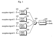
- FIG. 1 shows the block diagram of a currently used diversity reception equipment with MRC with four lines for receiving signals.
- input terminals 101 to 104 receive the signals
- phase shifters 105 to 108 arrange the carriers' phases equally
- adder 109 combines the signals
- decoder 110 decodes the combined signal.
- adder 109 combines the signals in linear form because each signal has been amplified in linear form.
- FIG. 2 shows an Inphase Quadrature plane figure representing how a current transmission equipment combines signals. For convenience's sake, it shows the case of combining two lines of signals.
- S1 and S2 represent reception signals.
- S1S and S1N respectively represent a signal element and a noise element of S1.
- S2S and S2N respectively represent a signal element and a noise element of S2.
- the level of each noise element is equal despite the size of received signal and the difference of receiving lines (hereinafter branches). That is why the reception signal in each branch is drawn as a point on the circumference with the same radius from signal elements S1S and S2S respectively (as
- signals received from each branch are combined in linear form, that is, S1 and S2 are combined in vector, and the combined signal is input in the decoder.
- MRC requires a very high efficiency in synchronizing the carrier phases when combining the signals
- DSP Digital Signal Processor
- A/D converter for combining the signal in linear form, A/D converter with wide dynamic range is required.
- a reception device with MRC has problems in its size and cost.
- MRC also have the following defect.
- MRC may be a most preferable combiner under such propagation condition as is affected by only the random disturbance like thermal noise because the received signals are just combined in linear form.
- MRC is vulnerable to interference waves such as the delay wave. Especially, when such waves are included in the signal received in a branch with high reception level, the signal is weighted much despite the bad quality, decreasing the receiving performance heavily.
- the first object of the present invention in consideration of the above mentioned problems, is to provide a diversity reception device with MRC in simple configuration, comprising only small-scale digital circuits suitable for IC, including a memory and an adder.
- the above object is achieved by a diversity reception device for weighting and combining a plurality of reception signals.
- the diversity reception device comprises: a plurality of phase demodulators for demodulating a phase of a respective one of the plurality of reception signals and outputting phase data consisting of a predetermined number of bits; a convertor having a first input port which receives the phase data, a second input port which receives a combination coefficient consisting of a predetermined number of bits, a first output port, a second output port, and a storage, for outputting predetermined values stored in a place in the storage specified by a combination of the phase data and the combination coefficient, from the first output port and the second output port upon input of the phase data and the combination coefficient, the predetermined values concerning respectively sine elements and cosine elements corresponding to the plurality of reception signals; a sine elements adder for adding up the predetermined values output from the first output port; and a cosine element adder for adding up the predetermined values output from the second output port.
- the plurality of phase demodulators each may comprise: a phase detector for detecting and outputting a phase of the respective one of the plurality of reception signals; a delay for delaying, one symbol time, data output from the phase detector; and a calculator for calculating a difference between data output from the phase detector and data output from the delay, and outputting a result as a phase difference data.
- a first storage and a second storage output predetermined values if reception signal and phase data output from phase demodulator are given. Then, by adding up the predetermined values for each reception signal, the received signals are combined to one. Therefore, the present reception device dispenses with expensive components such as DSP, and comprises only with small-scale digital circuits suitable for IC including a memory and an adder.
- the converter may comprise: a plurality of first storage, corresponding to the plurality of reception signals and storing calculation results obtained by a certain calculation on all the combinations of sine of the phase data multiplied by the combination coefficient, for fetching and outputting, upon entering of the phase data and the combination coefficient, one of the calculation results stored in a place specified by a combination of the phase data as a first address and the combination coefficient as a second address; and a plurality of second storage, corresponding to the plurality of reception signals and storing calculation results obtained by a certain calculation on all the combinations of cosine of the phase data multiplied by the combination coefficient, for fetching and outputting, upon entering of the phase data and the combination coefficient, one of the calculation results stored in a place specified by a combination of the phase data as a first address and the combination coefficient as a second address.
- the convertor may comprise: a first storage storing calculation results obtained by a certain calculation on all the combinations of sine of the phase data multiplied by the combination coefficient, for fetching and outputting, upon entering of the phase data and the combination coefficient, one of the calculation results stored in a place specified by a combination of the phase data as a first address and the combination coefficient as a second address; a second storage storing calculation results obtained by a certain calculation on all the combinations of cosine of the phase data multiplied by the combination coefficient, for fetching and outputting, upon entering of the phase data and the combination coefficient, one of the calculation results stored in a place specified by a combination of the phase data as a first address and the combination coefficient as a second address; a phase selector containing a plurality of input ports connected to the plurality of phase demodulator, and an output port connected to the first storage and to the second storage, for selecting a piece of phase data according to a certain instruction out of the phase data input to the plurality of input ports, and outputting the piece of phase data to the
- the first storage may store calculated results of sine of the phase data multiplied by the combination coefficient raised to a power of 2
- the second storage stores calculated results of cosine of the phase data multiplied by the combination coefficient raised to the power of 2.
- a plurality of signals are combined by a first storage and a second storage with a method of selecting the signals one by one. This enables to minimize the size and the cost of the diversity reception device.
- the second object of the present invention is to provide a diversity reception device that combines a plurality of signals avoiding the influence of interference waves like delay wave and outputs a high-quality signal.
- the diversity reception device may further comprise: a plurality of comparator, corresponding to the plurality of reception signals and containing an input port and an output port, for comparing a reception level input to the input port consisting of a predetermined number of bits with a predetermined value, and outputting a result from the outputting port; a plurality of likelihood detector, corresponding to the plurality of reception signals, for detecting a distance between the phase data and a decision point, and outputting the distance; and a plurality of outputs, corresponding to the plurality of reception signals, for outputting the reception level as the combination coefficient if the result output from the plurality of comparators shows that the reception level is less than the predetermined value, and outputting, as the combination coefficient, a predetermined value based on the distance output from the plurality of likelihood detectors multiplied by the reception level if the result shows that the reception level is not less than the predetermined value.
- a plurality of comparator corresponding to the plurality of reception signals and containing an input port and an output port, for
- the first storage may store calculated results of sine of the phase data multiplied by the combination coefficient
- the second storage stores calculated results of cosine of the phase data multiplied by the combination coefficient
- the diversity reception device may further comprise: a plurality of combination coefficient calculators, corresponding to the plurality of reception signals, for detecting the distance between the phase data and the decision point, and outputting, as the combination coefficient, a value obtained by performing a certain calculation on the detected distance.
- the present diversity reception devices detect the strength of the interference wave in each reception signal by a likelihood detector, and, based on the strength, determine how much each signal should be weighted. Unnecessary influence of interference wave can be eliminated by setting such a condition as the bigger the influence of the interference wave in a received signal is, the less weighted the signal is when combined.
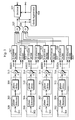
- FIG.3 illustrates the configuration of a diversity reception device with MRC in the first embodiment of the present invention.
- the device comprises phase demodulators 329-332, I-element ROMs 317-320, Q-element ROMs 321-324, I-element adder 325, Q-element adder 326, decision 327, and clock regenerator 328.
- Phase demodulators 329-332 comprise input terminals 301-304, phase detectors 305-308, phase delays 309-312, and phase adders 313-316 respectively, each as a whole is a differential detector of phase-detector type of Differential Phase Shift Keying (DPSK) modulation method.
- DPSK Differential Phase Shift Keying
- the reception signals digitalized by A/D converter or limiter, etc. enter through input terminals 301-304.
- Phase detectors 305-308 output detected phases in digital after comparing the phases of the signals input in input terminals 301-304 with the phase of the local oscillator that does not appear in the figures. That means, phase detectors 305-308 do not require any linear amplifier because only phase element, not the amplitude element, of the received signal is necessary.
- Phase delays 309-312 delay the detected phases output from phase detectors 305-308 1 symbolic time and output the delayed phases.
- 1 symbolic time indicates a time obtained from the period of the received signal multiplied by the exponent of 2 of the polyphase PSK (e.x., 2 for 4 phases (22), and 3 for 8 phases (23)).
- Phase adders 313-316 calculate the phase differences between the detected phases and the delayed phases and output the results as the phase data.
- the phase data provide phase data ⁇ k corresponding to branch k.
- I-element adder 325 totals the values output from I-element ROMs 317-320.
- Q-element adder 326 totals the values output from Q-element ROMs 321-324.
- Decision 327 synchronizing with the clock signal sent from clock regenerator 328, synthesizes a vector from the values from I-element adder 325 and Q-element adder 326, decides whether the result value is bigger or less than the preset threshold value, and outputs the decision result as decoded data.
- Clock regenerator 328 regenerates the clock signal synchronising with the data from I-element adder 325 and Q-element adder 326, and sends the clock signal to decision 327.
- FIG.4 is an IQ plane figure showing signals S1 and S2 input to the diversity reception device of FIG.1 and the combined signal by the present invention. For convenience's sake, only two received signals (S1 and S2) are selected for this figure.
- phase data ⁇ 1 and ⁇ 2 are sent to I-element ROMs 317 and 318 and Q-element ROMs 321 and 322.
- I-element adder 325 obtains I-element of the combined signal by adding S''1I and S''2I, represented as
- Q-element adder 326 obtains Q-element of the combined signal by adding S''1Q and S''2Q, represented as
- the combined signal by MRC is obtained, and decision 327, the final step, decodes the signal.
- RSSI2 is used as the weight coefficient when reception signals are combined.
- MRC diversity output MRC(n) is represented as
- phase data DDk of each branch is represented as Hence,
- MRC diversity output MRC(n) is obtained with
- MRC diversity reception device of the present invention can be composed with such small digital circuits suitable for IC as memory, adder, and shift register, dispensing with expensive DSP and the like. Furthermore, this invention realizes the non-linear amplification that takes a very simple composition on radio circuit because a signal input to the present device need not be linear. These elements bear a multiplier effect to decrease the cost of the components of the current device, and decrease the cost of the radio equipment as a whole.
- FIG.5 is a block diagram illustrating the configuration of the MRC diversity reception device in the second embodiment of the present invention.
- the present device differs from the diversity reception device of the first embodiment in that only two ROMs, I-element ROM 317 and Q-element ROM 321, are provided to cover all the four branches.
- the same components as those in the first embodiment have the same numbers in FIG.5.
- the present device differs from the diversity reception device of the first embodiment in that the present device additionally has timing generator 501, phase selector 502, reception level selector 503, latches 504 and 505, and delay 506.
- Phase selector 502 sequentially selects phase data sent from phase demodulators 329-332 synchronously with the clock signal sent from timing generator 501, receives phase data from the phase demodulator, and sends it to I-element ROM 317 and Q-element ROM 321.
- reception level selector 503 sequentially selects an input port out of a plural of input ports in 503 with the clock signal sent from timing generator 501, receives the reception level of the signal input in the port, and sends it to I-element ROM 317 and Q-element ROM 321. Phase selector 502 and reception level selector 503 select the same branch at the same timing according to the clock signal.
- I-element ROM 317 and Q-element ROM 321 output I-element and Q-element of each reception signal to I-element adder 325 and Q-element adder 326 respectively.
- 325 and 326 accumulate each sent element four times, and the results are stored in latches 504 and 505 respectively. Then, 325 and 326 are reset by the clock signal sent from delay 506.
- phase data and reception levels of four branches of the same reception signal are sent to I-element ROM 317 and Q-element ROM 321 respectively by time division, and the same combined signal as that of the first embodiment is obtained at last.
- the device of the first embodiment needs as many I-element ROMs and Q-element ROMs as there are branches, the device of the present embodiment has only one ROM for each element of the branch to achieve the same performance. This enables an even smaller and less-electricity device than the first embodiment.
- FIG.6 is a block diagram illustrating the configuration of a branch of the MRC diversity reception device in the third embodiment of the present invention.
- the present device differs from the diversity reception devices of the first and second embodiments in that the present device additionally has timing generator 601, offset 602, adder 603, and selector 605, and that two ROMs are replaced by storage 604.
- Offset 602 and selector 605 operate synchronously according to the clock signal sent from timing generator 601.
- any of such combinations as 0 and 64, 64 and 128, 128 and 192 and the like is output from offset 602.
- Adder 603 adds the above offset data to the phase data of each branch, and sends the result value to an address in storage 604.
- the operational values corresponding to I-element and Q-element stored in storage 604 are fetched alternately by time division and are used to calculate I-element and Q-element of the received signal.
- the device in the first and second embodiments require I-element ROM and Q-element ROM
- the device in the present embodiment has only one ROM to replace the above components achieving the same performance. This enables an even smaller and less-electricity device than the first and second embodiments.
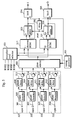
- FIG.7 is a block diagram illustrating the configuration of a diversity reception device in the fourth embodiment of the present invention.
- the present device differs from the diversity reception device of the first embodiment in that the present device additionally has combination coefficient calculators 701-704, and that I-element ROMs 705-708 and Q-element ROMs 709-712 operate differently.
- the same components as those in the first embodiment appear in FIG.7, having the same numbers, and are not explained here.
- Combination coefficient calculators 701-704 are ROMs storing combination coefficient values which are obtained by calculating all the possible distances between the decision point and the phase data.
- phase data is input from a phase demodulator 329, 330, 331, or 332 as an address to a respective combination coefficient calculator 701, 702, 703, or 704, combination coefficient Ck that corresponds to a distance between the decision point and the phase data is output.
- FIG.8 shows the eye-pattern of phase data at ⁇ /4 shift QPSK. It shows demodulated phases of the phase data synchronously taken. Distances L1 and L2 each indicate the likelihood of the decision point of each phase against the ideal decision point. The bigger the distance is, the more ideal the signal is, that is, the lower the rate of interference wave included in the reception signal is.
- I-element ROMs 705-708 store operational values of Ck ⁇ cos ⁇ k for all the combinations of combination coefficient Ck and phase data ⁇ k.
- I-element ROMs 705-708 output a calculation result of Ck ⁇ cos ⁇ k corresponding to the combination.
- Q-element ROMs 709-712 store operational values of Ck ⁇ sin ⁇ k for all the combinations of combination coefficient Ck and phase data ⁇ k.
- combination coefficient Ck and phase data ⁇ k as addresses are input from combination coefficient calculators 701-704 and phase adders 313-316 respectively.
- I-element ROMs 709-712 output calculation result of Ck ⁇ sin ⁇ k corresponding to the combination.
- FIG.9 is an IQ plane figure showing received signals and a combined signal obtained by the present device. For convenience's sake, only two received signals are shown in this figure.
- Phase demodulators 329 and 330 are differential detector of phase detection type. Therefore, signals S1 and S2 output from the above phase demodulators contain only ⁇ 1 and ⁇ 2 which are phase data of the received signals, and have no amplitude data. Since the signals S1 and S2 have the same size, on the IQ plane, they are represented as points on the same circumference whose center is the origin. These phase data ⁇ 1 and ⁇ 2 are sent to combination coefficient calculators 701 and 702, I-element ROMs 705 and 706, and Q-element ROMs 709 and 710.
- Combination coefficient calculators 701 and 702 calculate combination coefficients C1 and C2 which are weights used in combining received signals, and send the results to I-element ROMs 705 and 706, and Q-element ROMs 709 and 710.
- Q-element adder 326 obtains Q-element of the combined signal by adding S'1Q and S'2Q, as
- I-element and Q-element of the combined signal is obtained, and decision 327, final step, decodes the signal data.
- MRC diversity reception device of the present invention can compose such small digital circuits suitable for IC as memory, adder, and shift register, dispensing with expensive DSP and the like.
- the device of the present embodiment differs from MRC device in that it obtains a combined signal by weighting it with a coefficient based on the distance of the phase data not by weighting the reception signal level. In this way, the present device can remove the effect of interference wave because it less weights a reception signal when bigger interference wave is included in the reception signal.
- FIG.10 is a block diagram illustrating the configuration of a diversity reception device in the fifth embodiment of the present invention.
- the present device differs from the diversity reception device of the first embodiment in that the present device additionally has likelihood detectors 1001-1003 and combination coefficient controllers 1004-1007.
- the same components as those in the first embodiment appear in FIG.10, having the same numbers, and are not explained here.
- Likelihood detectors 1001-1003 detect the distance between the decision point and phase data output from phase demodulators 329-332, and send the results to combination coefficient controllers 1004-1007.
- Combination coefficient calculators 1004-1007 compose, as shown in FIG.11, comparator 1101, multiplication coefficient ROM 1103, and converter 1102.
- Comparator 1101 have in itself an input port and an output port, compare reception level consisting of the predetermined number of bits input to the input port with the predetermined value stored inside, and output the result from the output port.
- Multiplication coefficient ROM 1103 stores predetermined value of multiplication Ak ⁇ Rk which covers all the combinations of multiplication coefficient Ak, which is determined by distance Lk, and reception level Rk. Multiplication coefficient ROM 1103 selects a calculation result of Ak ⁇ Rk if distance Lk and reception level Rk are input as addresses, and send the selected value to converter 1102.
- Converter 1102 selects reception level Rk or Ak ⁇ Rk output from multiplication coefficient ROM 1103, and output the result as combination coefficient Ck.
- combination coefficient controller 1004-1007 shown in FIG.10.
- FIG.12 is a flowchart illustrating the operation of combination coefficient controllers 1004-1007.
- reception level Rk and distance Lk are input to combination coefficient controller 1004-1007 (step S1201), then comparator 1101 compares reception level Rk and the predetermined value (step S1202).
- reception level Rk is smaller than the predetermined value
- converter 1102 selects contact A and outputs reception level Rk as combination coefficient Ck (steps S1203 and S1205). If reception level Rk is small, it means that the S/N ratio is bad. In that case, even if distance Lk is short, it cannot be said that it is due to the effect of interference wave. Therefore, when reception level Rk is small, the combination signal is obtained by weighting only reception level Rk without considering distance Lk. That means a branch with small reception level Rk is treated the same as that in MRC diversity device.
- converter 1102 selects contact B and outputs Ak ⁇ Rk, output from multiplication coefficient ROM 1103, as combination coefficient Ck (steps S1204 and S1205).
- Ak takes a small value if reception level Rk is big and S/N ratio is good and Lk is small and there is strong interference wave. That means a branch with strong interference wave has a small combination coefficient, and the effect of interference wave is decreased.
- the present device works as MRC diversity device if the comparator uses predetermined comparison value Rk at its maximum, and that it works as a diversity device which weights multiplication coefficient if the comparator uses Rk at its minimum.
- the present device can compose small digital circuits suitable for IC as memory, adder, and shift register, dispensing with expensive DSP and the like. And the cost down of the whole radio equipment is possible with the present device.
- the device of the present embodiment differs from MRC device in that it obtains a combined signal by weighting it with a coefficient based on the distance of the phase data not by weighting the reception signal level.
- the present device can remove the effect of interference wave because it less weights a reception signal when bigger interference wave is included in the reception signal. Accordingly, the present signal combination method provides better combination signal than the current MRC.
Applications Claiming Priority (6)
| Application Number | Priority Date | Filing Date | Title |
|---|---|---|---|
| JP06101027A JP3091634B2 (ja) | 1994-05-16 | 1994-05-16 | ダイバーシチ装置 |
| JP10102794 | 1994-05-16 | ||
| JP101027/94 | 1994-05-16 | ||
| JP231518/94 | 1994-09-27 | ||
| JP23151894 | 1994-09-27 | ||
| JP06231518A JP3091649B2 (ja) | 1994-09-27 | 1994-09-27 | ダイバーシチ装置 |
Publications (3)
| Publication Number | Publication Date |
|---|---|
| EP0683571A2 true EP0683571A2 (de) | 1995-11-22 |
| EP0683571A3 EP0683571A3 (de) | 1997-07-16 |
| EP0683571B1 EP0683571B1 (de) | 2003-07-23 |
Family
ID=26441955
Family Applications (1)
| Application Number | Title | Priority Date | Filing Date |
|---|---|---|---|
| EP95107401A Expired - Lifetime EP0683571B1 (de) | 1994-05-16 | 1995-05-15 | Einrichtung zum Diversity-Empfang |
Country Status (6)
| Country | Link |
|---|---|
| US (3) | US5761252A (de) |
| EP (1) | EP0683571B1 (de) |
| CN (1) | CN1078409C (de) |
| CA (1) | CA2149364C (de) |
| DE (1) | DE69531325T2 (de) |
| MY (1) | MY113061A (de) |
Cited By (4)
| Publication number | Priority date | Publication date | Assignee | Title |
|---|---|---|---|---|
| GB2315196A (en) * | 1996-07-11 | 1998-01-21 | Nec Corp | Diversity combiner |
| GB2332124A (en) * | 1997-12-05 | 1999-06-09 | British Broadcasting Corp | Digital radio communication system |
| SG80579A1 (en) * | 1996-08-27 | 2001-05-22 | Nec Corp | Method of combining reception signal of diversity type radio device and diversity type radio device |
| EP1143676A1 (de) * | 1998-12-25 | 2001-10-10 | Sanyo Electric Co., Ltd. | Dekodierungsfehlerfreier diversitätsempfänger, sowie schaltung zur talzurückgewinnung für diversitätsempfänger |
Families Citing this family (49)
| Publication number | Priority date | Publication date | Assignee | Title |
|---|---|---|---|---|
| MY113061A (en) * | 1994-05-16 | 2001-11-30 | Sanyo Electric Co | Diversity reception device |
| JP3286885B2 (ja) * | 1995-11-07 | 2002-05-27 | 三菱電機株式会社 | タイミング再生手段及びダイバーシティ通信装置 |
| JP3162980B2 (ja) * | 1995-11-22 | 2001-05-08 | 三洋電機株式会社 | ダイバーシチ装置 |
| KR0168796B1 (ko) * | 1996-03-27 | 1999-02-01 | 김광호 | 다이버시티용 결합기에서 정규화 전압 발산 방지를 위한 정규화 회로 |
| CA2214743C (en) * | 1996-09-20 | 2002-03-05 | Ntt Mobile Communications Network Inc. | A frame synchronization circuit and communications system |
| JPH11112462A (ja) * | 1997-08-08 | 1999-04-23 | Sony Corp | デジタル放送の受信機 |
| US6389085B1 (en) * | 1998-01-14 | 2002-05-14 | Wavecom Electronics Inc. | Receiver combiner for spatial diversity digital communications |
| US6115930A (en) * | 1998-06-11 | 2000-09-12 | Fuji Photo Film Co., Ltd. | Method and laminated member for measuring gap dimension |
| US6061551A (en) | 1998-10-21 | 2000-05-09 | Parkervision, Inc. | Method and system for down-converting electromagnetic signals |
| US6091940A (en) | 1998-10-21 | 2000-07-18 | Parkervision, Inc. | Method and system for frequency up-conversion |
| US6694128B1 (en) | 1998-08-18 | 2004-02-17 | Parkervision, Inc. | Frequency synthesizer using universal frequency translation technology |
| US7515896B1 (en) | 1998-10-21 | 2009-04-07 | Parkervision, Inc. | Method and system for down-converting an electromagnetic signal, and transforms for same, and aperture relationships |
| US6370371B1 (en) | 1998-10-21 | 2002-04-09 | Parkervision, Inc. | Applications of universal frequency translation |
| US7039372B1 (en) | 1998-10-21 | 2006-05-02 | Parkervision, Inc. | Method and system for frequency up-conversion with modulation embodiments |
| US6049706A (en) | 1998-10-21 | 2000-04-11 | Parkervision, Inc. | Integrated frequency translation and selectivity |
| US6813485B2 (en) | 1998-10-21 | 2004-11-02 | Parkervision, Inc. | Method and system for down-converting and up-converting an electromagnetic signal, and transforms for same |
| US6560301B1 (en) | 1998-10-21 | 2003-05-06 | Parkervision, Inc. | Integrated frequency translation and selectivity with a variety of filter embodiments |
| US7236754B2 (en) | 1999-08-23 | 2007-06-26 | Parkervision, Inc. | Method and system for frequency up-conversion |
| US6542722B1 (en) | 1998-10-21 | 2003-04-01 | Parkervision, Inc. | Method and system for frequency up-conversion with variety of transmitter configurations |
| US6061555A (en) | 1998-10-21 | 2000-05-09 | Parkervision, Inc. | Method and system for ensuring reception of a communications signal |
| US6442130B1 (en) * | 1999-01-21 | 2002-08-27 | Cisco Technology, Inc. | System for interference cancellation |
| US6704558B1 (en) | 1999-01-22 | 2004-03-09 | Parkervision, Inc. | Image-reject down-converter and embodiments thereof, such as the family radio service |
| US6704549B1 (en) | 1999-03-03 | 2004-03-09 | Parkvision, Inc. | Multi-mode, multi-band communication system |
| US6449469B1 (en) * | 1999-03-01 | 2002-09-10 | Visteon Global Technologies, Inc. | Switched directional antenna for automotive radio receivers |
| US6308054B2 (en) * | 1999-03-02 | 2001-10-23 | Hitachi, Ltd. | Diversity wireless communication method and its wireless communication apparatus |
| US6879817B1 (en) | 1999-04-16 | 2005-04-12 | Parkervision, Inc. | DC offset, re-radiation, and I/Q solutions using universal frequency translation technology |
| US6853690B1 (en) | 1999-04-16 | 2005-02-08 | Parkervision, Inc. | Method, system and apparatus for balanced frequency up-conversion of a baseband signal and 4-phase receiver and transceiver embodiments |
| US7693230B2 (en) | 1999-04-16 | 2010-04-06 | Parkervision, Inc. | Apparatus and method of differential IQ frequency up-conversion |
| US7110444B1 (en) | 1999-08-04 | 2006-09-19 | Parkervision, Inc. | Wireless local area network (WLAN) using universal frequency translation technology including multi-phase embodiments and circuit implementations |
| US7065162B1 (en) | 1999-04-16 | 2006-06-20 | Parkervision, Inc. | Method and system for down-converting an electromagnetic signal, and transforms for same |
| US8295406B1 (en) | 1999-08-04 | 2012-10-23 | Parkervision, Inc. | Universal platform module for a plurality of communication protocols |
| JP2001230709A (ja) | 2000-02-17 | 2001-08-24 | Nec Shizuoka Ltd | ダイバーシチ受信装置 |
| US6714774B1 (en) * | 2000-02-24 | 2004-03-30 | Texas Instruments Incorporated | Antenna reception diversity in wireless communications |
| US7010286B2 (en) | 2000-04-14 | 2006-03-07 | Parkervision, Inc. | Apparatus, system, and method for down-converting and up-converting electromagnetic signals |
| US7454453B2 (en) | 2000-11-14 | 2008-11-18 | Parkervision, Inc. | Methods, systems, and computer program products for parallel correlation and applications thereof |
| US7855948B2 (en) * | 2001-09-05 | 2010-12-21 | Cisco Technology, Inc. | Interference mitigation in a wireless communication system |
| US6990059B1 (en) | 2001-09-05 | 2006-01-24 | Cisco Technology, Inc. | Interference mitigation in a wireless communication system |
| US7072427B2 (en) | 2001-11-09 | 2006-07-04 | Parkervision, Inc. | Method and apparatus for reducing DC offsets in a communication system |
| US7103118B2 (en) * | 2001-11-26 | 2006-09-05 | Dataradio Inc. | Vectorial combiner for diversity reception in RF tranceivers |
| FI20012581A0 (fi) * | 2001-12-27 | 2001-12-27 | Nokia Corp | Häiriönpoistomenetelmä kommunikaatiojärjestelmässä |
| US7379883B2 (en) | 2002-07-18 | 2008-05-27 | Parkervision, Inc. | Networking methods and systems |
| US7460584B2 (en) | 2002-07-18 | 2008-12-02 | Parkervision, Inc. | Networking methods and systems |
| US7006809B2 (en) * | 2003-05-06 | 2006-02-28 | Ami Semiconductor, Inc. | Adaptive diversity receiver architecture |
| US7499696B2 (en) * | 2003-11-26 | 2009-03-03 | Delphi Technologies, Inc. | Method to optimize hierarchical modulation for a diversity system |
| US7260370B2 (en) * | 2003-12-10 | 2007-08-21 | James June-Ming Wang | Wireless communication system using a plurality of antenna elements with adaptive weighting and combining techniques |
| US7046064B1 (en) * | 2004-04-02 | 2006-05-16 | Thomas Jefferson Runaldue | Clock generation with continuous phase |
| US7856215B2 (en) * | 2006-12-06 | 2010-12-21 | Broadcom Corp. | Method and system for using a multi-RF input receiver for diversity selection |
| CN102148787A (zh) * | 2010-02-10 | 2011-08-10 | 思亚诺移动芯片有限公司 | 用于降低或消除接收信号噪声的方法、电路和系统 |
| WO2012102258A1 (ja) * | 2011-01-26 | 2012-08-02 | ルネサスエレクトロニクス株式会社 | 判定帰還型等化器 |
Family Cites Families (8)
| Publication number | Priority date | Publication date | Assignee | Title |
|---|---|---|---|---|
| JPS5732535B2 (de) * | 1975-02-17 | 1982-07-12 | ||
| JPS5588452A (en) * | 1978-12-26 | 1980-07-04 | Nec Corp | Digital signal switching circuit for diversity receiver for digital radio communication |
| JP2756477B2 (ja) * | 1989-06-26 | 1998-05-25 | 日本電信電話株式会社 | 受信レベル適応形検波後合成ダイバーシチ受信回路 |
| US5280637A (en) * | 1991-09-18 | 1994-01-18 | Motorola, Inc. | Phase combining method and apparatus for use in a diversity receiver |
| US5321850A (en) * | 1991-10-09 | 1994-06-14 | Telefonaktiebolaget L M Ericsson | Diversity radio receiver automatic frequency control |
| US5465271A (en) * | 1993-08-20 | 1995-11-07 | General Electric Company | Post detection weighted vector combining diversity receivers using phase metrics for mobile and indoor radio channels |
| US5461646A (en) * | 1993-12-29 | 1995-10-24 | Tcsi Corporation | Synchronization apparatus for a diversity receiver |
| MY113061A (en) * | 1994-05-16 | 2001-11-30 | Sanyo Electric Co | Diversity reception device |
-
1995
- 1995-05-06 MY MYPI95001209A patent/MY113061A/en unknown
- 1995-05-15 DE DE69531325T patent/DE69531325T2/de not_active Expired - Fee Related
- 1995-05-15 EP EP95107401A patent/EP0683571B1/de not_active Expired - Lifetime
- 1995-05-15 CA CA002149364A patent/CA2149364C/en not_active Expired - Fee Related
- 1995-05-16 CN CN95106512A patent/CN1078409C/zh not_active Expired - Fee Related
- 1995-05-16 US US08/441,993 patent/US5761252A/en not_active Expired - Fee Related
-
1998
- 1998-05-21 US US09/082,582 patent/US5901187A/en not_active Expired - Fee Related
-
1999
- 1999-03-19 US US09/272,570 patent/US6161001A/en not_active Expired - Lifetime
Non-Patent Citations (1)
| Title |
|---|
| None |
Cited By (11)
| Publication number | Priority date | Publication date | Assignee | Title |
|---|---|---|---|---|
| GB2315196A (en) * | 1996-07-11 | 1998-01-21 | Nec Corp | Diversity combiner |
| GB2315196B (en) * | 1996-07-11 | 1999-02-17 | Nec Corp | Diversity combining |
| US5889826A (en) * | 1996-07-11 | 1999-03-30 | Nec Corporation | Apparatus and method for diversity combining |
| AU717652B2 (en) * | 1996-07-11 | 2000-03-30 | Nec Corporation | Diversity combining |
| SG80579A1 (en) * | 1996-08-27 | 2001-05-22 | Nec Corp | Method of combining reception signal of diversity type radio device and diversity type radio device |
| GB2332124A (en) * | 1997-12-05 | 1999-06-09 | British Broadcasting Corp | Digital radio communication system |
| GB2332124B (en) * | 1997-12-05 | 2002-07-17 | British Broadcasting Corp | Digital radio communication system |
| EP1143676A1 (de) * | 1998-12-25 | 2001-10-10 | Sanyo Electric Co., Ltd. | Dekodierungsfehlerfreier diversitätsempfänger, sowie schaltung zur talzurückgewinnung für diversitätsempfänger |
| EP1143676A4 (de) * | 1998-12-25 | 2003-05-28 | Sanyo Electric Co | Dekodierungsfehlerfreier diversitätsempfänger, sowie schaltung zur talzurückgewinnung für diversitätsempfänger |
| AU776028B2 (en) * | 1998-12-25 | 2004-08-26 | Kyocera Corporation | Diversity receiver free from decoding error, and clock regeneration circuit for diversity receiver |
| US6901124B1 (en) | 1998-12-25 | 2005-05-31 | Sanyo Electric Co., Ltd. | Diversity receiving apparatus that prevents judgement errors during decoding and a clock generating circuit for a diversity circuit that prevents judgement errors during decoding |
Also Published As
| Publication number | Publication date |
|---|---|
| CA2149364C (en) | 2005-05-10 |
| CA2149364A1 (en) | 1995-11-17 |
| EP0683571B1 (de) | 2003-07-23 |
| CN1078409C (zh) | 2002-01-23 |
| EP0683571A3 (de) | 1997-07-16 |
| DE69531325D1 (de) | 2003-08-28 |
| MY113061A (en) | 2001-11-30 |
| US6161001A (en) | 2000-12-12 |
| CN1121664A (zh) | 1996-05-01 |
| DE69531325T2 (de) | 2004-05-13 |
| US5761252A (en) | 1998-06-02 |
| US5901187A (en) | 1999-05-04 |
Similar Documents
| Publication | Publication Date | Title |
|---|---|---|
| EP0683571B1 (de) | Einrichtung zum Diversity-Empfang | |
| US5109392A (en) | Diversity receiver arrangement for digital signals | |
| US7116999B2 (en) | Mobile communications receiving apparatus and method | |
| US7167695B2 (en) | Diversity receiver and method of diversity reception | |
| CA2412924C (en) | Vectorial combiner for diversity reception in rf transceivers | |
| JP3091634B2 (ja) | ダイバーシチ装置 | |
| JP3091649B2 (ja) | ダイバーシチ装置 | |
| JP2000031874A (ja) | 適応アレーダイバーシティ受信機 | |
| JP3182376B2 (ja) | ダイバーシチ受信装置 | |
| CA2269740C (en) | Diversity receiver | |
| JPH10256967A (ja) | 検波後ダイバーシチ受信回路 | |
| JPH1168647A (ja) | ダイバーシチ受信機 | |
| US6901124B1 (en) | Diversity receiving apparatus that prevents judgement errors during decoding and a clock generating circuit for a diversity circuit that prevents judgement errors during decoding | |
| JP3037184B2 (ja) | 遅延検波復調方式 | |
| JPH0923178A (ja) | ダイバーシチ受信機 | |
| JP3611933B2 (ja) | 送信ダイバーシチを行なう送受信装置 | |
| JPH0327626A (ja) | 受信レベル適応形検波後合成ダイバーシチ受信回路 | |
| JPH06268559A (ja) | ダイバーシチ受信機 | |
| JP2021083061A (ja) | 無線受信装置 | |
| JPH10229360A (ja) | 検波後ダイバーシチ受信回路 | |
| KR20050086783A (ko) | 수신된 신호의 상관을 최소화하기 위한 장치, 모듈 및프로그램 제품 | |
| JPH10233722A (ja) | ダイバーシティ受信機 | |
| JPH09162791A (ja) | ダイバーシティ受信機 | |
| JP2000115043A (ja) | ダイバーシチ受信方法およびダイバーシチ受信機 | |
| JPH1041926A (ja) | ダイバーシチ受信装置 |
Legal Events
| Date | Code | Title | Description |
|---|---|---|---|
| PUAI | Public reference made under article 153(3) epc to a published international application that has entered the european phase |
Free format text: ORIGINAL CODE: 0009012 |
|
| AK | Designated contracting states |
Kind code of ref document: A2 Designated state(s): DE FR GB |
|
| PUAL | Search report despatched |
Free format text: ORIGINAL CODE: 0009013 |
|
| AK | Designated contracting states |
Kind code of ref document: A3 Designated state(s): DE FR GB |
|
| 17P | Request for examination filed |
Effective date: 19970814 |
|
| 17Q | First examination report despatched |
Effective date: 20010309 |
|
| GRAH | Despatch of communication of intention to grant a patent |
Free format text: ORIGINAL CODE: EPIDOS IGRA |
|
| GRAH | Despatch of communication of intention to grant a patent |
Free format text: ORIGINAL CODE: EPIDOS IGRA |
|
| GRAA | (expected) grant |
Free format text: ORIGINAL CODE: 0009210 |
|
| AK | Designated contracting states |
Designated state(s): DE FR GB |
|
| REG | Reference to a national code |
Ref country code: GB Ref legal event code: FG4D |
|
| REF | Corresponds to: |
Ref document number: 69531325 Country of ref document: DE Date of ref document: 20030828 Kind code of ref document: P |
|
| ET | Fr: translation filed | ||
| PLBE | No opposition filed within time limit |
Free format text: ORIGINAL CODE: 0009261 |
|
| STAA | Information on the status of an ep patent application or granted ep patent |
Free format text: STATUS: NO OPPOSITION FILED WITHIN TIME LIMIT |
|
| 26N | No opposition filed |
Effective date: 20040426 |
|
| PGFP | Annual fee paid to national office [announced via postgrant information from national office to epo] |
Ref country code: DE Payment date: 20080522 Year of fee payment: 14 |
|
| PGFP | Annual fee paid to national office [announced via postgrant information from national office to epo] |
Ref country code: GB Payment date: 20080521 Year of fee payment: 14 |
|
| REG | Reference to a national code |
Ref country code: FR Ref legal event code: TP |
|
| GBPC | Gb: european patent ceased through non-payment of renewal fee |
Effective date: 20090515 |
|
| REG | Reference to a national code |
Ref country code: FR Ref legal event code: ST Effective date: 20100129 |
|
| PG25 | Lapsed in a contracting state [announced via postgrant information from national office to epo] |
Ref country code: FR Free format text: LAPSE BECAUSE OF NON-PAYMENT OF DUE FEES Effective date: 20090602 |
|
| PGFP | Annual fee paid to national office [announced via postgrant information from national office to epo] |
Ref country code: FR Payment date: 20080514 Year of fee payment: 14 |
|
| PG25 | Lapsed in a contracting state [announced via postgrant information from national office to epo] |
Ref country code: GB Free format text: LAPSE BECAUSE OF NON-PAYMENT OF DUE FEES Effective date: 20090515 |
|
| PG25 | Lapsed in a contracting state [announced via postgrant information from national office to epo] |
Ref country code: DE Free format text: LAPSE BECAUSE OF NON-PAYMENT OF DUE FEES Effective date: 20091201 |