EP0681235B1 - Anordnung zum Summieren von Produkten zweier gleichen oder unterschiedlichen Signale - Google Patents
Anordnung zum Summieren von Produkten zweier gleichen oder unterschiedlichen Signale Download PDFInfo
- Publication number
- EP0681235B1 EP0681235B1 EP95106093A EP95106093A EP0681235B1 EP 0681235 B1 EP0681235 B1 EP 0681235B1 EP 95106093 A EP95106093 A EP 95106093A EP 95106093 A EP95106093 A EP 95106093A EP 0681235 B1 EP0681235 B1 EP 0681235B1
- Authority
- EP
- European Patent Office
- Prior art keywords
- signal
- clock rate
- output
- arrangement according
- multiplier
- Prior art date
- Legal status (The legal status is an assumption and is not a legal conclusion. Google has not performed a legal analysis and makes no representation as to the accuracy of the status listed.)
- Expired - Lifetime
Links
Images


Classifications
-
- G—PHYSICS
- G06—COMPUTING OR CALCULATING; COUNTING
- G06G—ANALOGUE COMPUTERS
- G06G7/00—Devices in which the computing operation is performed by varying electric or magnetic quantities
- G06G7/12—Arrangements for performing computing operations, e.g. operational amplifiers specially adapted therefor
- G06G7/16—Arrangements for performing computing operations, e.g. operational amplifiers specially adapted therefor for multiplication or division
- G06G7/161—Arrangements for performing computing operations, e.g. operational amplifiers specially adapted therefor for multiplication or division with pulse modulation, e.g. modulation of amplitude, width, frequency, phase or form
-
- G—PHYSICS
- G01—MEASURING; TESTING
- G01R—MEASURING ELECTRIC VARIABLES; MEASURING MAGNETIC VARIABLES
- G01R21/00—Arrangements for measuring electric power or power factor
- G01R21/133—Arrangements for measuring electric power or power factor by using digital technique
-
- G—PHYSICS
- G06—COMPUTING OR CALCULATING; COUNTING
- G06F—ELECTRIC DIGITAL DATA PROCESSING
- G06F7/00—Methods or arrangements for processing data by operating upon the order or content of the data handled
- G06F7/60—Methods or arrangements for performing computations using a digital non-denominational number representation, i.e. number representation without radix; Computing devices using combinations of denominational and non-denominational quantity representations, e.g. using difunction pulse trains, STEELE computers, phase computers
- G06F7/602—Methods or arrangements for performing computations using a digital non-denominational number representation, i.e. number representation without radix; Computing devices using combinations of denominational and non-denominational quantity representations, e.g. using difunction pulse trains, STEELE computers, phase computers using delta-sigma sequences
-
- G—PHYSICS
- G06—COMPUTING OR CALCULATING; COUNTING
- G06J—HYBRID COMPUTING ARRANGEMENTS
- G06J1/00—Hybrid computing arrangements
Definitions
- the invention relates to an arrangement for summing products of the same two or different signals according to the preamble of claim 1.
- the arrangement is used e.g. B. in electricity meters, for determining electricity and / or RMS voltage values, correlations, averaged electrical power and / or Energy values.
- the latter are known to be equal to a sum of more current ones Performance values, which in turn are each a product of a current one Voltage value and an associated current current value.
- GB 2 167 619 describes an arrangement for summing products of two signals At least one of the signals is described on a signal input one with a led first clock frequency operated sigma-delta modulator, the output of which is connected by two signal inputs of a multiplier.
- the invention is based, with at least approximately maintaining the task the classic multiplication achievable accuracy, an arrangement of the input to implement the type mentioned, which does not multiply two R-bit operands, but only simple shift and algebraic addition operations in the faster clock frequency require, e.g. B. a calculation of an effective value of a current in a Dynamic range of 1: 1000 with an accuracy of 0.5% possible with little effort is.
- the arrangement according to the invention is particularly advantageous if the multiplications are based on a special semiconductor chip to be realized.
- a first signal u [t] or i [t] is multiplied by a second identical or different signal u [t] or i [t] or f [t].
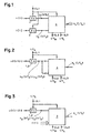
- At least one of the signals u [t] or i [t] is routed to a signal input of a sigma-delta modulator 1 or 2 operated at a first clock frequency 1 / T S , the output of which is multiplied by at least one of two signal inputs / Adding element 3 is connected.
- the signal u [t] is e.g. B. an electrical voltage
- the two signals are different time-functional signals u [t] and i [t] which each have an associated sigma-delta signal, operated at the first clock frequency 1 / T S Modulators 1 and 2 are guided.
- the outputs of the two sigma-delta modulators 1 and 2 are each connected to one of the two signal inputs of the multiplier / adder 3.
- the time-functional signal u [t] is thus via the sigma-delta modulator 1 to a first of the two signal inputs and the time-functional signal i [t] via the sigma-delta modulator 2 to a second of the two signal inputs of the multiplier / adder.
- the two signals are the same time-functional signals u [t] and u [t] or i [t] and i [t], one of which is connected to the signal input of the sigma-delta Modulator 1 or 2 is guided.
- the output of the latter is connected to the two signal inputs of the multiplier / adder 3.
- the two same time-functional signals u [t] and u [t] or i [t] and i [t] are multiplied with one another in the arrangement according to the invention such that the square u 2 [t] or i 2 [t] des relevant time-functional signal u [t] or i [t] is generated.
- this is first signal — a previously known time-functional signal u [t] or i [t] and the second Signal a previously known time-variable function f [t].
- the first signal is u [t] or i [t] led to the signal input of the associated sigma-delta modulator 1 or 2.
- the output of the latter is with one of the two signal inputs of the multiplier / adder 3 connected.
- One-bit or multi-bit digital values of the known time-variable function f [t] are in turn on the other of the two signal inputs of the multiplier / adder 3 led.
- the values of the known time-variable function f [t] are not always in the form of a 1-bit stream are available and are then connected via a bus connection as multi-bit digital values the relevant signal input of the multiplier / adder 3 supplied, the is then designed as a bus input.
- the signal u [t] or i [t] over the Sigma-delta modulator 1 or 2 as a 1-bit current to the first signal input of the Multiplier / adder 3 supplied while z.
- B. Multi-bit digital values of the function f [t] are fed to the second signal input.
- the Multiplication / addition z.
- B the determination of correlations.
- the multiplier / adder 3 is fed in all variants via separate clock inputs with three clock signals CL1, CL2 and CL3.
- the sigma-delta modulators 1 and 2 are each fed with the clock signal CL1, the frequency of which is the first clock frequency 1 / T S.
- the time-functional signals u [t] and i [t] are sampled in the associated sigma-delta modulator 1 or 2 with the first clock frequency 1 / T S.
- the frequency of CL2 is the second clock frequency 1 / T M and that of CL3 is the third clock frequency 1 / T L.
- the first clock frequency 1 / T S is thus greater than the second clock frequency 1 / T M and the latter in turn is greater than the third clock frequency 1 / T L.
- Signals of the clock frequency 1 / T S subsequently have an index S
- signals of the clock frequency 1 / T M have an index M
- a signal of the clock frequency 1 / T L have an index L.
- the output signals of the sigma-delta modulators 1 and 2 are included x S [hT S ] or y S [hT S ] and the output signal of the multiplier / adder 3 is denoted by z L [jT L ] (see FIGS. 1 to 3).
- Each sigma-delta modulator 1 or 2 of the three variants is preferably a second-order sigma-delta modulator.
- FIG. 4 shows such a second-order sigma-delta modulator 1 or 2, known per se, whose forward path in the order given consists of a series connection of a first difference-forming element 4, a first gain element 5, and a first integrator 6 , a second difference-forming element 7, a second amplifying element 8, a second integrator 9 and a 1-bit analog / digital converter 10, the latter preferably being a keyed comparator and in the two difference-forming elements 4 and 7 for the series connection the plus input is used.
- a zero order hold element (“Zero order hold" ZOH) is connected to the minus inputs of the two difference-forming elements 4 and 7.
- a clock input of the 1-bit analog / digital converter 10 is fed by the clock signal CL1 with the first clock frequency 1 / T S.
- their input signals are weighted with a factor K 1 or K 2 .
- Q is the level of the quantization level of the 1-bit analog / digital converter 10.
- the signals u S [hT S ] and i S [hT S ] are in the first approximation, with the exception of a delay of one or two clocks, the non-quantized the clock frequency 1 / T S sampled signals u [t] or i [t].
- the signals ⁇ Su [hT S] and ⁇ Si [hT S] are represented by the quantization error sequences caused at the output of sigma-delta modulator 1 and 2, respectively, which are known to each have a differentiating character.
- Inequalities (2) and (2a) indicate the scope of the input signal u [t] and i [t], respectively.
- the time-functional signals u [t] and i [t] are each converted into a 1-bit stream x S [hT S in the sigma-delta modulator 1 or 2 ] or y S [hT S ] of the clock frequency 1 / T S converted, which a two-valued signal ⁇ + Q / 2, -Q / 2 ⁇ or z.
- B. represents ⁇ +1, -1 ⁇ , which only consists of the two values + Q / 2 and -Q / 2 or +1 and -1.
- the output signal x S [hT S ] or y S [hT S ] of the sigma-delta modulator 1 or 2 is thus a sequence of two-valued pulses.
- Fig. 5 is within the multiplier / adder 3 one, z. B. second signal input via a operated at the first clock frequency 1 / T S first decimation filter 12 to a first input of an adder 13 and the other, for. B. first signal input via a first clock frequency 1 / T S operated delay arrangement 14 to a second input of the adder 13.
- the voltage u [t] is multiplied by the associated current i [t] to determine the sum of the corresponding instantaneous powers (see FIG.
- the signal i [t] which generally has a greater dynamic range than the voltage u [ t], preferably to the second signal input of the multiplier / adder 3 and thus to the decimation filter 12, while the voltage u [t] is preferably supplied to the first signal input, ie the delay arrangement 14.
- the accuracy is better than that when determining the effective values of the current i [t] (see FIG. 2), since the large dynamic range is only present with one operand, namely the current i [t].
- the third variant see FIG.
- the signal u [t] or i [t] is preferably fed to the first signal input of the multiplier / adder 3 and thus to the delay arrangement 14, while the eg multi-bit digital values of the Function f [t] are preferably fed to the second signal input and thus to the decimation filter 12.
- the adder 13 is used to implement algebraic additions and its output is routed via a divider 17 to a signal input of a second decimation filter 18 operated at the second clock frequency 1 / T M , the output of which forms an output of the multiplier / adder 3.
- the division factor of the divider 17 is equal to the ratio T M / T S of the fast first clock frequency 1 / T S of the clock signal CL1 to the medium-fast second clock frequency 1 / T M of the clock signal CL2, ie equal to the first oversampling rate N.
- the decimation filters 12 and 18 are digital filters, the output signal of which is read out with a lower clock frequency than the one with which their input signal is processed in the actual digital filter. This is indicated symbolically in FIG. 5 in that the decimation filters 12 and 18 are each represented by an input function block 12a or 18a and a downstream output function block 12b or 18b.
- the input function blocks 12a and 18a each represent the actual digital filter, while the output function blocks 12b and 18b indicate the readout process, which is symbolically represented by a read switch contact 12c and 18c, respectively.
- the input function block 12a has a clock input which is fed by the clock signal CL1 with the fast first clock frequency 1 / T S
- the output function block 12b has a clock input which is clocked by the clock signal CL2 with a slower, namely the medium-fast second clock frequency 1 / T M is fed.
- the input function block 18a has a clock input which is fed by the clock signal CL2 with the medium-fast second clock frequency 1 / T M
- the output function block 18b has a clock input which is fed by the clock signal CL3 with the slow third clock frequency 1 / T L .
- the output function blocks 12b and 18b of the decimation filters 12 and 18 are thus operated with a lower clock frequency 1 / T M or 1 / T L than the associated input function block 12a or 18a, which with the clock frequency 1 / T S or 1 / T M is operated, the second clock frequency 1 / T M and the third clock frequency 1 / T L each serving to read the output signal of the first and second decimation filters 12 and 18, respectively.
- the decimation filter 12 is preferably a sinc filter of order K and length N, ie its length is preferably equal to the first oversampling rate N, that is to say the ratio T M / T S of the fast first clock frequency 1 / T S to the medium-fast second clock frequency 1 / T M.
- the decimation filter 18 is preferably a first-order sinc filter of length W, ie its length is preferably equal to the second oversampling rate W, that is to say the ratio T L / T M of the medium-fast second clock frequency 1 / T M for the slow third clock frequency 1 / T L.
- the delay arrangement 14 consists either of a delay element 15 operated at the first clock frequency 1 / T S or of a series circuit 15; 16 of the delay element 15 operated at the first clock frequency 1 / T S and a downstream circuit, likewise at the first clock frequency 1 / T S operated decimation-free digital filter 16.
- Each clock input of the delay element 15 and, if present, the digital filter 16 is fed by the clock signal CL1 with the fast clock frequency 1 / T S.
- the decimation-free digital filter 16 (“sliding filter”) is preferably a first-order sinc filter of length four.
- the rapidly clocked signal x S [hT S ] is delayed in the delay element 15 by a delay period D, so that a quickly clocked delayed signal d S [hT S ] appears at its output.
- the delay period D of the delay element 15 is preferably equal to K (N-1) / 2. If a digital filter 16 is present, the quickly clocked delayed signal d S [hT S ] is also converted by low-pass filtering in the digital filter 16 into a low-pass filtered delayed signal v S [hT S ], resulting in a low frequency compared to the fast clock frequency 1 / T s Filtered useful signal and the quantization noise is partially suppressed.
- Low-pass filtering of the rapidly clocked signal y S [hT S ] in the decimation filter 12 can also filter out a useful signal which is low in frequency with respect to the fast clock frequency 1 / T s , and the quantization noise can be partially suppressed.
- y M [kT M ] With the medium-fast clock frequency 1 / T M , a low-pass filtered signal y M [kT M ] is obtained at the output of the decimation filter 12, which has a much better accuracy than the original signal, since a clever choice of the clock frequencies 1 / T S and 1 / T M as well as the filter characteristics can achieve a very high accuracy.
- the values of y M [kT M ] are e.g. B. represented by 16 bits.
- the larger the first oversampling rate N is selected, the stronger the suppression of the quantization influence and the greater the accuracy of the converted signal. If the quantization error of the 1-bit analog / digital converter 10 is regarded as idealized noise which is equally distributed in the interval [-Q / 2, Q / 2], then its variance is ⁇ 2 ⁇ Q 2 12th
- the variance of the quantization error at the output of the sigma-delta modulator 2 is:
- i M [kT M ] is just equal to i [t].
- the decimated signal i M [kT M ] is somewhat distorted by the low-pass characteristic of the decimation filter 12, ie linearly phase-shifted and slightly damped.
- the transfer function of the decimation filter 12 of order K and length N can be both recursive and non-recursive:
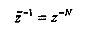
- z -1 is the delay in the fast cycle 1 / T S.
- the 1-bit current x S [hT S ] supplied by the sigma-delta modulator 1 with the possible values ⁇ 1, -1 ⁇ , as already mentioned, is delayed by the delay time D, and then in the digital filter 16, if available, to be low-pass filtered at a fast rate.
- the delay of the series circuit 15; 16 should be adapted as well as possible to the delay caused by the decimation filter 12. The smallest possible delay is advantageous in terms of implementation effort.
- the series circuit 15; 16 of the delay element 15 and the digital filter 16 always works in the fast clock 1 / T S. It should be noted that the digital filter 16 operates as a so-called “sliding filter” and that no decimation to the slower, medium-fast clock frequency 1 / T M is carried out.
- the output sequence v S [ hT S ] of the digital filter 16 is very simple, although a favorable filter effect is achieved.
- v S [ hT S ] (1/4) ⁇ d S [ hT S ] + d S [( H -1) T S ] + d S [( H -2) T S ] + d S [( H -3) T S ]
- the medium-fast signal y M [kT M ] obtained at the output of the decimation filter 12 is driven in the adder 13 with the fast signal v s [ hT s ] of the clock frequency 1 / T S. Since the latter can only assume the values +1, +1/2, 0, -1/2 and -1 in the selected example, only the operations “shift”, “add / subtract (+ 1/2, - 1/2) "and” Add / Subtract (+1, -1) ". In addition, shifts and algebraic additions with subsequent decimation to the slow clock frequency 1 / T M are carried out in the adder 13.
- the adder 13 has the task of correctly controlling the signal y M [kT M ] coming from the decimation filter 12 during N fast clocks of the frequency 1 / T S. The process will be explained using two examples.
- the output signal of the divider 17 is relatively imprecise and must be averaged by z M [kT M ] in the downstream second decimation filter 18 over at least one period of the fundamental frequency of the time-functional signal u [t] or i [t] or f [t] and a subsequent decimation to the slow clock frequency 1 / T L are further processed, which gives the signal z L [jT L ] at the output of the second decimation filter 18, which then equals the sum of the squares or products appearing at the output of the divider 17 during this time is in the second decimation filter 18 z.
- Sinc filtering of the first order with subsequent decimation to the slow clock frequency 1 / T L 1 / (WT M ), and a division by W.
- the time-functional signals u [t] and i [t] are z. B. proportional to a 50 Hz mains voltage or a 50 Hz mains current. The period of their basic frequency is then 20ms.
- the accuracy of the multiplication can hardly be improved by averaging over several periods.
- a greater averaging effect is achieved, so that results can be achieved which are close to those of conventional direct multiplication and addition. Since the 1-bit current pattern at the output of the sigma-delta modulator 1 or 2 is not repeated regularly due to the initial conditions, the error sequences at the output of the two filters 12 and 16 will not be repeated exactly.
- the square of the effective value of the relevant signal u [t] or i [t] appears at the output of the multiplier / adder 3. If it is not the square of the RMS value, but the RMS value itself that is to be determined, the output of the multiplier / adder 3 is connected to an input of a square root extraction member 19 (see FIG. 5). Subsequent to the decimation to the slow clock frequency 1 / T L in the second decimation filter 18, the square root extraction element 19 from the output signal z L [jT L ] of the second decimation filter 18 by square root extraction z. B. the effective value U eff of the time-functional signal u [t] is determined. The square root extraction in the square root extraction element 19 takes place with the slow clock frequency 1 / T L.
Landscapes
- Engineering & Computer Science (AREA)
- Physics & Mathematics (AREA)
- Theoretical Computer Science (AREA)
- General Physics & Mathematics (AREA)
- Mathematical Physics (AREA)
- Software Systems (AREA)
- Computer Hardware Design (AREA)
- Power Engineering (AREA)
- Evolutionary Computation (AREA)
- Fuzzy Systems (AREA)
- Automation & Control Theory (AREA)
- Computational Mathematics (AREA)
- Computing Systems (AREA)
- Mathematical Analysis (AREA)
- Mathematical Optimization (AREA)
- Pure & Applied Mathematics (AREA)
- General Engineering & Computer Science (AREA)
- Compression, Expansion, Code Conversion, And Decoders (AREA)
- Container Filling Or Packaging Operations (AREA)
- Beverage Vending Machines With Cups, And Gas Or Electricity Vending Machines (AREA)
Description
- Fig. 1
- ein Blockschaltbild einer ersten Variante einer Anordnung,
- Fig. 2
- ein Blockschaltbild einer zweiten Variante der Anordnung,
- Fig. 3
- ein Blockschaltbild einer dritten Variante der Anordnung,
- Fig. 4
- ein Blockschaltbild eines bekannten Sigma-Delta-Modulators zweiter Ordnung und
- Fig. 5
- ein Blockschaltbild eines erfindungsgemässen Multiplizier/Addier-Gliedes.


- K = 1:
- rechtecksförmig,
- K = 2:
- dreiecksförmig und
- K = 3:
- parabolförmig mit einem abgeflachten Mittelstück.




Claims (13)
- Anordnung zum Summieren von Produkten zweier zeitfunktionaler Signale (u[t], i[t] bzw. u[t], u[t] bzw. i[t], i[t] bzw. u[t], f[t] bzw. i[t], f[t]), wobei mindestens eines der Signale (u[t] bzw. i[t]) auf einen Signaleingang eines mit einer ersten Taktfrequenz (1/TS) betriebenen Sigma-Delta-Modulators (1 bzw. 2) geführt ist, dessen Ausgang mit mindestens einem von zwei Signaleingängen eines Multiplizier/Addier-Gliedes (3) verbunden ist, dadurch gekennzeichnet, dass innerhalb des Multiplizier/Addier-Gliedes (3) der eine Signaleingang über ein mit der ersten Taktfrequenz (1/TS) betriebenes erstes Dezimationsfilter (12) auf einen ersten Eingang eines, Additionsgliedes (13) geführt ist und der andere Signaleingang über eine mit der ersten Taktfrequenz (1/TS) betriebene Verzögerungsanordnung (14) auf einen zweiten Eingang des Additionsgliedes (13) geführt ist dass ein Ausgang des letzteren über ein Dividierglied (17) auf einen Signaleingang eines mit einer zwelten Taktfrequenz (1/TM) betriebenen zweiten Dezimationsfilters (18) geführt ist dessen Ausgang einen Ausgang des Multiplizier/Addier-Gliedes (3) bildet, und dass die zweite Taktfreguenz (1/TM) sowie eine dritte Taktfreguenz, (1/TL) dem Lesen eines Ausgangssignals des ersten beziehungsweise zweiten Dezimationsfilters (12 bzw. 18) dient, wobei die erste Taktfreguenz (1/TS) grösser als die zweite Taktfrequenz (1/TM) und die letztere grösser als die dritte Taktfreguenz (1/TL) ist.
- Anordnung nach Anspruch 1, dadurch gekennzeichnet, dass die beiden Signale (u[t], i[t]) unterschiedliche zeitfunktionale Signale sind, die auf einen Signaleingang je eines zugehörigen, jeweils mit der ersten Taktfrequenz (1/TS) betriebenen Sigma-Delta-Modulators (1 bzw. 2) geführt sind, und dass die Ausgänge der beiden Sigma-Delta-Modulatoren (1, 2) mit je einem der beiden Signaleingänge des Multiplizier/Addier-Gliedes (3) verbunden sind.
- Anordnung nach Anspruch 1, dadurch gekennzeichnet, dass die beiden Signale (u[t], u[t] bzw. i[t], i[t]) gleiche zeitfunktionale Signale sind, wovon eines auf den Signaleingang des Sigma-Delta-Modulators (1 bzw. 2) geführt ist, und dass der Ausgang des letzteren mit den beiden Signaleingängen des Multiplizier/Addier-Gliedes (3) verbunden ist.
- Anordnung nach Anspruch 3, dadurch gekennzeichnet, dass ein Ausgang des Multiplizier/Addier-Gliedes (3) mit einem Eingang eines Quadratwurzelziehungs-Gliedes (19) verbunden ist.
- Anordnung nach Anspruch 1, dadurch gekennzeichnet, dass ein erstes der beiden Signale (u[t], f[t] bzw. i[t], f[t]) ein im voraus nicht bekanntes zeitfunktionales Signal (u[t] bzw. i[t]) und das andere der beiden Signale (u[t], f[t] bzw. i[t], f[t]) eine bekannte zeitvariable Funktion (f[t]) ist, dass das erste Signal (u[t] bzw. i[t]) auf den Signaleingang des Sigma-Delta-Modulators (1 bzw. 2) geführt ist, dessen Ausgang mit dem einen der beiden Signaleingänge des Multiplizier/Addier-Gliedes (3) verbunden ist, und dass Einbit- oder Mehrbit-Digitalwerte der bekannten zeitvariablen Funktion (f[t]) auf den anderen der beiden Signaleingänge des Multiplizier/Addier-Gliedes (3) geführt sind, der als Bus-Eingang ausgebildet ist.
- Anordnung nach einem der Ansprüche 1 bis 5, dadurch gekennzeichnet, dass jeder Sigma-Delta-Modulator (1 bzw. 2) ein Sigma-Delta-Modulator zweiter Ordnung ist.
- Anordnung nach einem der Ansprüche 1 bis 6, dadurch gekennzeichnet, dass das erste Dezimationsfilter (12) ein Sinc-Filter der Ordnung K und einer Länge N ist, welche letztere gleich dem Verhältnis (TM/TS) der ersten zur zweiten Taktfrequenz (1/TS bzw. 1/TM) ist.
- Anordnung nach einem der Ansprüche 1 bis 7, dadurch gekennzeichnet, dass der Teilungsfaktor des Dividiergliedes (17) gleich dem Verhältnis (TM/TS) der ersten zur zweiten Taktfrequenz (1/TS bzw.1/TM) ist.
- Anordnung nach einem der Ansprüche 1 bis 8, dadurch gekennzeichnet, dass das zweite Dezimationsfilter (18) ein Sinc-Filter erster Ordnung der Länge W ist, welche letztere gleich dem Verhältnis (TL/TM) der zweiten zur dritten Taktfrequenz (1/TM bzw. 1/TL) ist.
- Anordnung nach einem der Ansprüche 1 bis 9, dadurch gekennzeichnet, dass die Verzögerungsanordnung (14) aus einem mit der ersten Taktfrequenz (1/TS) betriebenen Verzögerungsglied (15) besteht.
- Anordnung nach einem der Ansprüche 1 bis 10, dadurch gekennzeichnet, dass die Verzögerungsanordnung (14) aus einer Reihenschaltung (15;16) eines mit der ersten Taktfrequenz (1/TS) betriebenen Verzögerungsgliedes (15) und eines nachgeschalteten, ebenfalls mit der ersten Taktfrequenz (1/TS) betriebenen dezimationslosen Digitalfilters (16) besteht.
- Anordnung nach Anspruch 11, dadurch gekennzeichnet, dass das dezimationslose Digitalfilter (16) ein Sinc-Filter erster Ordnung der Länge vier ist.
- Anordnung nach einem der Ansprüche 10 bis 12, dadurch gekennzeichnet, dass die Verzögerungsdauer (D) des Verzögerungsgliedes (15) gleich K(N-1)/2 ist.
Applications Claiming Priority (3)
| Application Number | Priority Date | Filing Date | Title |
|---|---|---|---|
| CH01411/94A CH689471A5 (de) | 1994-05-05 | 1994-05-05 | Anordnung zum Summieren von Produkten zweier gleichen oder unterschiedlichen Signale. |
| CH1411/94 | 1994-05-05 | ||
| CH141194 | 1994-05-05 |
Publications (3)
| Publication Number | Publication Date |
|---|---|
| EP0681235A2 EP0681235A2 (de) | 1995-11-08 |
| EP0681235A3 EP0681235A3 (de) | 1995-12-27 |
| EP0681235B1 true EP0681235B1 (de) | 2001-12-05 |
Family
ID=4209825
Family Applications (1)
| Application Number | Title | Priority Date | Filing Date |
|---|---|---|---|
| EP95106093A Expired - Lifetime EP0681235B1 (de) | 1994-05-05 | 1995-04-24 | Anordnung zum Summieren von Produkten zweier gleichen oder unterschiedlichen Signale |
Country Status (5)
| Country | Link |
|---|---|
| US (1) | US5745063A (de) |
| EP (1) | EP0681235B1 (de) |
| AT (1) | ATE210312T1 (de) |
| CH (1) | CH689471A5 (de) |
| DE (1) | DE59509893D1 (de) |
Cited By (1)
| Publication number | Priority date | Publication date | Assignee | Title |
|---|---|---|---|---|
| DE10311777A1 (de) * | 2003-03-18 | 2004-10-28 | Thomas Schoch | Verfahren und Vorrichtung zur elektrischen Leistungsmessung |
Families Citing this family (12)
| Publication number | Priority date | Publication date | Assignee | Title |
|---|---|---|---|---|
| JPH09189918A (ja) | 1995-12-29 | 1997-07-22 | Xerox Corp | 光アクティブセルアレイ |
| US5782665A (en) | 1995-12-29 | 1998-07-21 | Xerox Corporation | Fabricating array with storage capacitor between cell electrode and dark matrix |
| US5862069A (en) * | 1996-07-12 | 1999-01-19 | Analog Devices, Inc. | Four quadrant multiplying apparatus and method |
| DE19630605A1 (de) * | 1996-07-29 | 1998-02-05 | Tech Gmbh Antriebstechnik Und | Multiplikationsschaltung für Leistungs-Meßgerät |
| DE19639410A1 (de) | 1996-09-25 | 1998-04-02 | Siemens Ag | Meßeinrichtung für elektrische Leistung |
| US6396877B1 (en) * | 1998-01-27 | 2002-05-28 | Agere Systems Guardian Corp. | Method and apparatus for combining serial data with a clock signal |
| DE60215463T2 (de) * | 2002-05-22 | 2007-02-08 | Freescale Semiconductor, Inc., Austin | Analog-Digital-Wandler Anordnung und Methode |
| US8180169B2 (en) * | 2008-02-27 | 2012-05-15 | Xerox Corporation | System and method for multi-scale sigma filtering using quadrature mirror filters |
| US8416880B2 (en) * | 2008-03-31 | 2013-04-09 | Nxp B.V. | Digital modulator |
| US8208753B2 (en) * | 2008-04-11 | 2012-06-26 | Xerox Corporation | Method and system for noise level detection in image data |
| CN103091550B (zh) * | 2013-01-08 | 2015-02-11 | 北京优科利尔能源设备有限公司 | 一种宽电压与大电流同步隔离采样直流功率计 |
| US9525430B1 (en) * | 2015-12-03 | 2016-12-20 | Djuro G. Zrilic | Method and apparatus for full-wave rectification of delta-sigma modulated signals |
Family Cites Families (7)
| Publication number | Priority date | Publication date | Assignee | Title |
|---|---|---|---|---|
| GB2167619A (en) * | 1984-11-24 | 1986-05-29 | Crest Energy Scan Ltd | Wattmeter circuit |
| JP3012887B2 (ja) * | 1989-03-13 | 2000-02-28 | 日本テキサス・インスツルメンツ株式会社 | 信号変換装置 |
| JP2832619B2 (ja) * | 1989-09-29 | 1998-12-09 | ジーイー横河メディカルシステム株式会社 | ディジタルrf方式の超音波診断装置 |
| US5148167A (en) * | 1990-04-06 | 1992-09-15 | General Electric Company | Sigma-delta oversampled analog-to-digital converter network with chopper stabilization |
| US5208594A (en) * | 1991-05-02 | 1993-05-04 | Ricoh Company, Ltd. | Signal processor that uses a delta-sigma modulation |
| JP3104108B2 (ja) * | 1992-09-07 | 2000-10-30 | ソニー株式会社 | アナログ/デジタルコンバータ |
| US5625358A (en) * | 1993-09-13 | 1997-04-29 | Analog Devices, Inc. | Digital phase-locked loop utilizing a high order sigma-delta modulator |
-
1994
- 1994-05-05 CH CH01411/94A patent/CH689471A5/de not_active IP Right Cessation
-
1995
- 1995-04-24 AT AT95106093T patent/ATE210312T1/de active
- 1995-04-24 EP EP95106093A patent/EP0681235B1/de not_active Expired - Lifetime
- 1995-04-24 DE DE59509893T patent/DE59509893D1/de not_active Expired - Lifetime
-
1997
- 1997-06-02 US US08/867,205 patent/US5745063A/en not_active Expired - Lifetime
Cited By (2)
| Publication number | Priority date | Publication date | Assignee | Title |
|---|---|---|---|---|
| DE10311777A1 (de) * | 2003-03-18 | 2004-10-28 | Thomas Schoch | Verfahren und Vorrichtung zur elektrischen Leistungsmessung |
| DE10311777B4 (de) * | 2003-03-18 | 2005-10-20 | Thomas Schoch | Verfahren, Messsystem und Vorrichtung zur elektrischen Leistungsmessung |
Also Published As
| Publication number | Publication date |
|---|---|
| ATE210312T1 (de) | 2001-12-15 |
| EP0681235A2 (de) | 1995-11-08 |
| CH689471A5 (de) | 1999-04-30 |
| US5745063A (en) | 1998-04-28 |
| EP0681235A3 (de) | 1995-12-27 |
| DE59509893D1 (de) | 2002-01-17 |
Similar Documents
| Publication | Publication Date | Title |
|---|---|---|
| EP0052847B1 (de) | Verfahren und Schaltungsanordnung zur Umsetzung der Abtastfrequenz einer Abtastfolge unter Umgehung der Konversion in ein kontinuierliches Signal | |
| DE3120914C2 (de) | ||
| DE4203879A1 (de) | Verfahren zur umwandlung eines messsignals und eines referenzsignals in ein ausgangssignal, sowie konverter zur durchfuehrung des verfahrens | |
| DE69631420T2 (de) | Verfahren und vorrichtung zur schätzung von nichtlinearität | |
| DE2728939A1 (de) | Vorrichtung und verfahren zum selektiven messen von intermodulationsverzerrung | |
| DE69212337T2 (de) | Sigma-Delta-Modulator für einen Digital/Analog-Umsetzer mit Wackelsignal | |
| DE3124924A1 (de) | Rekursives digitales tiefpassfilter | |
| DE69422650T2 (de) | Als dreistufiges transversales Filter anwendbare digitale Filterschaltung | |
| EP0681235A2 (de) | Anordnung zum Summieren von Produkten zweier gleichen oder unterschiedlichen Signale | |
| DE19521609B4 (de) | Dezimationsfilter mit wählbarem Dezimationsverhältnis und Verfahren zur Dezimationsfilterung | |
| DE2831059C2 (de) | Integrierender Kodeumsetzer | |
| DE102011116217A1 (de) | Verwendung eines multilevel-pulsweitenmodulierten Signals zur Realzeit-Rauschauslöschung | |
| DE3705209C2 (de) | ||
| DE3621737C2 (de) | ||
| EP0215810A1 (de) | Schaltungsanordnung zur mittelwertbildung. | |
| DE68912544T2 (de) | Rechteckiges angepasstes filter für variablen takt. | |
| DE19521610A1 (de) | Dezimationsfilter unter Verwendung einer Nullfüllschaltung zur Lieferung eines wählbaren Dezimationsverhältnisses | |
| DE69312281T2 (de) | A/d wandler | |
| DE2804915C2 (de) | ||
| DE68913967T2 (de) | Sigma-Delta-Konverter mit einer Dämpfungsfunktion sowie einer Übertragungsfunktion, die unempfindlich gegenüber Fehlanpassungen der Anstiegs- und Abfallzeiten der Schaltelemente ist. | |
| DE19510656B4 (de) | Schaltungsanordnung und Verfahren zum Filtern quantisierter elektrischer Signale | |
| DE3922469C2 (de) | ||
| DE3621446A1 (de) | Geraet zum digitalen verarbeiten von kontinuierlichen bitstroemen | |
| EP0609707B1 (de) | Verfahren zur Momentanfrequenz-Detektion | |
| DE102005023909B3 (de) | Digitaler Phasenregelkreis und Verfahren zur Korrektur von Störanteilen in einem Phasenregelkreis |
Legal Events
| Date | Code | Title | Description |
|---|---|---|---|
| PUAI | Public reference made under article 153(3) epc to a published international application that has entered the european phase |
Free format text: ORIGINAL CODE: 0009012 |
|
| PUAL | Search report despatched |
Free format text: ORIGINAL CODE: 0009013 |
|
| AK | Designated contracting states |
Kind code of ref document: A2 Designated state(s): AT CH DE FR GB LI |
|
| AK | Designated contracting states |
Kind code of ref document: A3 Designated state(s): AT CH DE FR GB LI |
|
| 17P | Request for examination filed |
Effective date: 19960201 |
|
| RAP1 | Party data changed (applicant data changed or rights of an application transferred) |
Owner name: SIEMENS METERING AG |
|
| 17Q | First examination report despatched |
Effective date: 20000704 |
|
| GRAG | Despatch of communication of intention to grant |
Free format text: ORIGINAL CODE: EPIDOS AGRA |
|
| GRAG | Despatch of communication of intention to grant |
Free format text: ORIGINAL CODE: EPIDOS AGRA |
|
| GRAH | Despatch of communication of intention to grant a patent |
Free format text: ORIGINAL CODE: EPIDOS IGRA |
|
| GRAH | Despatch of communication of intention to grant a patent |
Free format text: ORIGINAL CODE: EPIDOS IGRA |
|
| GRAA | (expected) grant |
Free format text: ORIGINAL CODE: 0009210 |
|
| AK | Designated contracting states |
Kind code of ref document: B1 Designated state(s): AT CH DE FR GB LI |
|
| REF | Corresponds to: |
Ref document number: 210312 Country of ref document: AT Date of ref document: 20011215 Kind code of ref document: T |
|
| REG | Reference to a national code |
Ref country code: CH Ref legal event code: EP |
|
| REG | Reference to a national code |
Ref country code: GB Ref legal event code: IF02 |
|
| GBT | Gb: translation of ep patent filed (gb section 77(6)(a)/1977) |
Effective date: 20011211 |
|
| REF | Corresponds to: |
Ref document number: 59509893 Country of ref document: DE Date of ref document: 20020117 |
|
| ET | Fr: translation filed | ||
| PLBE | No opposition filed within time limit |
Free format text: ORIGINAL CODE: 0009261 |
|
| STAA | Information on the status of an ep patent application or granted ep patent |
Free format text: STATUS: NO OPPOSITION FILED WITHIN TIME LIMIT |
|
| 26N | No opposition filed | ||
| REG | Reference to a national code |
Ref country code: CH Ref legal event code: PFA Owner name: LANDIS+GYR AG Free format text: SIEMENS METERING AG#FELDSTRASSE 1#6300 ZUG (CH) -TRANSFER TO- LANDIS+GYR AG#FELDSTRASSE 1#6300 ZUG (CH) |
|
| REG | Reference to a national code |
Ref country code: CH Ref legal event code: NV Representative=s name: OK PAT AG PATENTE MARKEN LIZENZEN |
|
| REG | Reference to a national code |
Ref country code: FR Ref legal event code: CD |
|
| REG | Reference to a national code |
Ref country code: CH Ref legal event code: NV Representative=s name: RENTSCH & PARTNER |
|
| REG | Reference to a national code |
Ref country code: CH Ref legal event code: PCAR Free format text: RENTSCH & PARTNER;FRAUMUENSTERSTRASSE 9, POSTFACH 2441;8022 ZUERICH (CH) |
|
| REG | Reference to a national code |
Ref country code: CH Ref legal event code: PFA Owner name: LANDIS+GYR AG Free format text: LANDIS+GYR AG#FELDSTRASSE 1#6300 ZUG (CH) -TRANSFER TO- LANDIS+GYR AG#FELDSTRASSE 1#6300 ZUG (CH) |
|
| REG | Reference to a national code |
Ref country code: CH Ref legal event code: NV Representative=s name: WEINMANN ZIMMERLI, CH |
|
| PGFP | Annual fee paid to national office [announced via postgrant information from national office to epo] |
Ref country code: GB Payment date: 20140430 Year of fee payment: 20 |
|
| PGFP | Annual fee paid to national office [announced via postgrant information from national office to epo] |
Ref country code: AT Payment date: 20140425 Year of fee payment: 20 Ref country code: FR Payment date: 20140428 Year of fee payment: 20 Ref country code: CH Payment date: 20140425 Year of fee payment: 20 Ref country code: DE Payment date: 20140627 Year of fee payment: 20 |
|
| REG | Reference to a national code |
Ref country code: CH Ref legal event code: PCOW Free format text: NEW ADDRESS: THEILERSTRASSE 1, 6301 ZUG (CH) |
|
| REG | Reference to a national code |
Ref country code: DE Ref legal event code: R071 Ref document number: 59509893 Country of ref document: DE |
|
| REG | Reference to a national code |
Ref country code: CH Ref legal event code: PL |
|
| REG | Reference to a national code |
Ref country code: GB Ref legal event code: PE20 Expiry date: 20150423 |
|
| REG | Reference to a national code |
Ref country code: AT Ref legal event code: MK07 Ref document number: 210312 Country of ref document: AT Kind code of ref document: T Effective date: 20150424 |
|
| PG25 | Lapsed in a contracting state [announced via postgrant information from national office to epo] |
Ref country code: GB Free format text: LAPSE BECAUSE OF EXPIRATION OF PROTECTION Effective date: 20150423 |